EP0840251A2 - Smart carte et méthode de fabrication - Google Patents
Smart carte et méthode de fabrication Download PDFInfo
- Publication number
- EP0840251A2 EP0840251A2 EP97117872A EP97117872A EP0840251A2 EP 0840251 A2 EP0840251 A2 EP 0840251A2 EP 97117872 A EP97117872 A EP 97117872A EP 97117872 A EP97117872 A EP 97117872A EP 0840251 A2 EP0840251 A2 EP 0840251A2
- Authority
- EP
- European Patent Office
- Prior art keywords
- layer
- dielectric material
- smartcard
- conductive
- conductive plate
- Prior art date
- Legal status (The legal status is an assumption and is not a legal conclusion. Google has not performed a legal analysis and makes no representation as to the accuracy of the status listed.)
- Granted
Links
Images
Classifications
-
- G—PHYSICS
- G06—COMPUTING; CALCULATING OR COUNTING
- G06K—GRAPHICAL DATA READING; PRESENTATION OF DATA; RECORD CARRIERS; HANDLING RECORD CARRIERS
- G06K19/00—Record carriers for use with machines and with at least a part designed to carry digital markings
- G06K19/06—Record carriers for use with machines and with at least a part designed to carry digital markings characterised by the kind of the digital marking, e.g. shape, nature, code
- G06K19/067—Record carriers with conductive marks, printed circuits or semiconductor circuit elements, e.g. credit or identity cards also with resonating or responding marks without active components
- G06K19/07—Record carriers with conductive marks, printed circuits or semiconductor circuit elements, e.g. credit or identity cards also with resonating or responding marks without active components with integrated circuit chips
- G06K19/077—Constructional details, e.g. mounting of circuits in the carrier
- G06K19/07749—Constructional details, e.g. mounting of circuits in the carrier the record carrier being capable of non-contact communication, e.g. constructional details of the antenna of a non-contact smart card
- G06K19/0775—Constructional details, e.g. mounting of circuits in the carrier the record carrier being capable of non-contact communication, e.g. constructional details of the antenna of a non-contact smart card arrangements for connecting the integrated circuit to the antenna
-
- G—PHYSICS
- G06—COMPUTING; CALCULATING OR COUNTING
- G06K—GRAPHICAL DATA READING; PRESENTATION OF DATA; RECORD CARRIERS; HANDLING RECORD CARRIERS
- G06K19/00—Record carriers for use with machines and with at least a part designed to carry digital markings
- G06K19/06—Record carriers for use with machines and with at least a part designed to carry digital markings characterised by the kind of the digital marking, e.g. shape, nature, code
- G06K19/067—Record carriers with conductive marks, printed circuits or semiconductor circuit elements, e.g. credit or identity cards also with resonating or responding marks without active components
- G06K19/07—Record carriers with conductive marks, printed circuits or semiconductor circuit elements, e.g. credit or identity cards also with resonating or responding marks without active components with integrated circuit chips
- G06K19/077—Constructional details, e.g. mounting of circuits in the carrier
- G06K19/07749—Constructional details, e.g. mounting of circuits in the carrier the record carrier being capable of non-contact communication, e.g. constructional details of the antenna of a non-contact smart card
- G06K19/07773—Antenna details
- G06K19/07777—Antenna details the antenna being of the inductive type
- G06K19/07779—Antenna details the antenna being of the inductive type the inductive antenna being a coil
- G06K19/07783—Antenna details the antenna being of the inductive type the inductive antenna being a coil the coil being planar
Definitions
- This invention relates, in general, to electronic components and, more particularly, to smartcards and methods of making the same.
- Smartcards are electronic components that have been developed to help facilitate high volume consumer transactions. For example, smartcards are used to record the number of fares on a bus pass. When a consumer boards a bus, the smartcard is placed in a smartcard reader and one credit is deducted from the consumer's account.
- contactless smartcards operate by simply placing the smartcard within close proximity to a smartcard reader. Contactless smartcards do not require the smartcard to be placed in a reader so the processing of the transaction can be expedited.
- One application for contactless smartcards is in toll booths. Each properly equipped automobile has a contactless smartcard and, as the automobile pass through the toll booth, a smartcard reader uses radio frequency (RF) transmissions to energize the card and deduct one fare from the consumer's account.
- RF radio frequency
- Typical contactless smartcards contain a semiconductor device which is used to store account information and to process each transaction.
- Contactless smartcards also have an antennae that is formed by wrapping a wire in a spiral pattern. The RF power collected by the antennae charges a discrete capacitor to power the semiconductor device and to ensure that the smartcard operates at the proper frequency.
- the present invention provides a novel process for forming a smartcard.
- a smartcard is an electronic component assembly capable of storing information pertaining to a consumer carrying the smartcard.
- the process described hereinbelow forms a capacitive structure as part of a laminate layer that becomes the smartcard.
- the smartcard comprises a sequence of individual layers that can be formed separately and then pressed together to form the laminate layer.
- One advantage of this process is that it obviates the need to bond discrete capacitors to the smartcard. This improves the flexibility of the smartcard, and thus, the reliability of the smartcard.
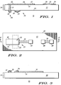
- FIG. 1 is an enlarged cross-sectional view of a smartcard 10 at an early stage in the fabrication process in accordance with the present invention.
- a layer of dielectric material 11, hereinafter referred to as dielectric layer 11, is used to form one of the layers in a laminate structure that becomes smartcard 10.
- Dielectric layer 11 provides the dielectric material of a capacitor structure 23 that replaces conventional discrete capacitors.
- Dielectric layer 11 also acts as a substrate upon which other structures and layers are formed.
- dielectric layer 11 has a dielectric constant ranging from about 3 to 30 and is formed using materials such as polytetrafluoroethylene, epoxy glass materials, polyimide, quartz, kevelar, liquid crystal polymer (LCP) or the like.
- the dielectric constant of the material used to provide dielectric layer 11 can be adjusted by adding a filler material such as ceramic, silica, artificial diamond, or the like.
- Dielectric layer 11 has a thickness 14, which is used to adjust the electrical characteristics of capacitive structure 23.
- the thickness 14 of dielectric layer 11 ranges from about 50 microns to 500 microns.
- a hole 24 is drilled through dielectric layer 11 from a top surface 12 to a bottom surface 13.
- hole 24 is used to provide an electrical connection through smartcard 10.
- Hole 24 contains a conductive material 15 such as copper, gold, nickel, aluminum, or the like using techniques such as electroplating or chemical vapor deposition.
- Conductive plate 21 is formed on the top surface 12 and conductive plate 22 is formed on the bottom surface 13 of dielectric layer 11 to form capacitive structure 23.
- Conductive plates 21 and 22, along with bonding pads 27-29 and interconnect lines 25 and 26, are patterned from a conductive layer (not shown) formed on the top surface 12 and the bottom surface 13 of dielectric layer 11.
- This conductive layer can be formed using a variety of techniques such as sputtering, electroplating, chemical vapor deposition, or by spreading a thin foil film on top surface 12 and bottom surface 13.
- This conductive layer can be made from a variety of materials such as aluminum, copper, gold, nickel, chrome, tungsten, and can also comprise a combination of materials such as sputtered seed layer of nickel and an electroplated layer chrome and copper.
- the conductive layer is patterned an etched using conventional techniques such as a patterned layer of photoresist and a reactive ion etch (RIE) or wet etching process.
- RIE reactive ion etch
- bonding material 20 is formed on conductive plates 22 and bonding material 18 is formed below the opening of hole 24 so that it is in electrical contact with conductive material 15.
- bonding materials 18 and 20 are used to provide electrical connection to other layers below dielectric layer 11.
- bonding material 20 can be used to electrically connect conductive plate 22 of capacitive structure 23 to an antennae formed below dielectric layer 11. This particular example will be illustrated shortly.
- bonding materials 18 and 20 are materials that form thermal compression bonds such as gold. It should be understood that other conductive materials such as nickel, solder paste, conductive epoxy, aluminum, or copper could also be used.
- FIG. 2 is an enlarged top view of dielectric layer 11 and section lines 1-1 are used to indicate the view provided in FIG. 1 in relationship to that shown in FIG. 2.
- Bonding pads 27 and 28 are used to electrically connect an electronic component (not shown) to capacitive structure 23.
- the electrical connection between bonding pad 27 and conductive plate 21 is provided by interconnect line 26.
- Bonding pad 29 is used to electrically connect the electronic component to any structures that might be above or below dielectric layer 11. Electrical connection between the electronic component and bonding pad 29 is provided by interconnect line 25.
- the relative size and location of conductive plate 22 in relationship to conductive plate 21 is shown in FIG. 2 as a dashed line.
- the portion of conductive plate 21 that overlaps dielectric layer 11 and conductive plate 22 forms capacitive structure 23 (see FIG. 1).
- the overlap is shown in FIG. 2 as area 19.
- the effective capacitance value of capacitive structure 23 is determined by the amount of overlap (area 19), the thickness 14 of dielectric layer 11, and the dielectric constant of dielectric layer 11. It should be appreciated that all three of these variables can be adjusted to allow flexibility in the size, location, and effective capacitance value of capacitor structure 23.
- dielectric layer 11 also has an outer edge 39 which defines its surface area.
- the surface area of dielectric layer 11 depends on a number of factors such as the final size of smartcard 10 and the capacitance necessary to form capacitive structure 23.
- dielectric layer 11 has a surface area of at least 1 millimeter.
- Conductive plate 21 also has a surface area as indicated by outer edge 38.
- dielectric layer 11 is not only used to provide dielectric material to capacitive structure 23, but is also used to provide flexibility to smartcard 10 and support for structures formed on dielectric layer 11 such as bonding pads 27 and 28.
- the surface area of dielectric layer 11 is greater than the surface area of conductive plate 21. It should also be understood that in some embodiments, the surface area of dielectric layer 11 can be equal to the surface area of conductive plate 21.
- FIG. 3 is an enlarged cross-sectional view of dielectric layer 30 which has a top surface 31 and a thickness 33, which preferably ranges from about 50 microns to 500 microns.
- dielectric layer 30 has a dielectric constant ranging from about 3 to 15 and is formed using materials such as polytetrafluoroethylene, epoxy glass materials, polyimide, liquid crystal polymers, or the like.
- the dielectric constant of the material used to provide dielectric layer 11 can be adjusted by adding a filler material such as ceramic, silica, artificial diamond, or the like.
- antennae 32 is formed on a top surface 31 of dielectric layer 30.
- antennae 32 is patterned from a layer of conductive material (not shown) that is patterned into the appropriate shape so that antennae 32 can receive a radio frequency (RF) signal to provide an electrical current to smartcard 10.
- RF radio frequency
- One method for forming antennae 32 forms a conductive layer made from materials such as copper, nickel/gold, aluminum, or the like, which is deposited onto top surface 31 using an electroplating, sputtering, or chemical vapor deposition process. It is also possible to form the conductive layer from a sequence of layers each having a different composition. For example, sputtering a layer of copper and then using an electroplating process to form a layer of nickel.
- the conductive layer can also be formed by placing a thin foil of conductive material onto top surface 31. The conductive layer is then patterned using conventional
- a mask layer (not shown), such as photoresist, is deposited onto the conductive layer.
- the mask layer has a pattern so that portions of the conductive layer are exposed and other portions are protected by the mask layer.
- An etch process is then used to remove the exposed portions of the conductive layer thus patterning the conductive layer into antennae 32.
- Conventional etch process such as reactive ion etching (RIE) or wet etch solutions can be used.
- RIE reactive ion etching
- wet etch solutions can be used.
- the type of etch used depends on the composition of the conductive layer used to form antennae 32.
- bonding materials 34 and 35 are formed on antennae 32 to provide electrical connection to layers overlying dielectric layer 30.
- the placement and size of bonding materials 34 and 35 depends on the electrical connections that are required to form smartcard 10.
- bonding materials 34 and 35 can be used to electrically couple antennae 32 to conductive plate 22 and conductive material 15 as is shown in the discussion to follow.
- Bonding materials 34 and 35 are preferably made from materials that readily form thermal compression bonds such as gold. It should be understood that other conductive materials such as nickel, solder paste, aluminum, conductive epoxy, or copper can be used to form bonding materials 34 and 35.
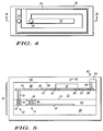
- FIG. 4 is an enlarged top view of dielectric layer 30.
- FIG. 4 illustrates one method for patterning antennae 32 so that it can receive an RF signal.
- antennae preferably has a spiral pattern made of a thin conductive material that revolves around itself.
- the spiral configuration of antennae 32 can be varied in both pitch and number of revolutions in the spiral pattern to optimize the response antennae 32 has to a particular radio frequency.
- Section lines 2-2 are provided in FIG. 4 to illustrate the cross-sectional view of FIG. 3.
- a dashed line 70 is used to indicate the surface area of antennae 32. All of the spiral pattern of antennae 32 is contained within the dashed line 70. In comparison to the preferred embodiment illustrated in FIG. 2, the surface area of dielectric layer 11 is greater than the surface area, dashed line 70, of antennae 32. It should also be understood that in an alternate embodiment not illustrated, the surface area of antenna 32 can be equal to the surface area of dielectric layer 11.
- FIG. 5 is an enlarged cross-sectional view of smartcard 10 after further processing.
- a layer of insulating material 45 such as polyimide, bondply, prepeg, unclad polytetrafluoroethylene, or the like is placed over dielectric layer 30.
- insulating layer 45 has openings 71 and 72 to allow bonding material 34 and 35 (see FIG. 3) to pass through insulating layer 45 to electrically couple to overlying structures.
- Dielectric layer 11 is positioned over insulating layer 45 so that bonding material 18 (see FIG. 1) aligns with bonding material 35 and so that bonding material 20 aligns with bonding material 34.
- a pressing operation is performed to permanently bond dielectric layer 30, insulating layer 45, and dielectric layer 11 together to form a portion of a laminate layer 77.
- One method for bonging these layers together applies a pressure ranging from about 50 pounds per square inch (PSI) to 500 PSI so dielectric layer 30 is forced towards dielectric layer 11 and vice versa.
- PSI pounds per square inch
- the layers are heated to a temperature ranging from about 400 degrees Celsius (°C) to 800°C for about 1 hour to 4 hours.
- This pressing operation allows bonding materials 20 and 34 to permanently bond and form contact 40 that passes through opening 71 in insulating layer 45 and electrically connects conductive plate 22 to antennae.
- Bonding materials 18 and 35 form contact 41 that passes through opening 72 in insulating layer 45 and electrically connects antennae 32 to conductive material 15, which in turn, is electrically connected to conductive plate 21.
- an additional insulating layer 50 can be bonded to the top surface 12 of dielectric layer 11 as part of laminate layer 77.
- Insulating layer 50 can be used to provide insulation between the conductive portions on dielectric layer 11 (i.e. conductive plate 21) and an electronic component 51.
- Insulating layer 50 can be made from a variety of materials such as poly vinyl chloride (PVC), thin FR-4, polyester, or polyimide depending on the electrical characteristics that are required.
- PVC poly vinyl chloride
- a similar pressing operation as described above can be used to permanently bond insulating layer 50 to dielectric layer 11.
- Insulating layer 50 has a cavity 75 that exposes portions of bonding pads 27 and 28, which are used to electrically connect to electronic component 51 in cavity 75.
- Electronic component 51 can be a variety of devices depending of the functional requirements of smartcard 10.
- electronic component 51 can be a semiconductor device, an integrated circuit, an optical electronic component, a microprosessor, a microcontroller, or the like.
- Conventional bonding techniques can be used to electrically and physically connect electronic component 51 to bonding pads 27 and 28.
- insulating layer 50 can have a hole 53 that is filled with a conductive material 54 to electrically connect bonding pad 29 on dielectric layer 11 to structures formed on or over the top surface 80 of insulating layer 50.
- a layer of resistive material 55 such as tungsten, polysilicon, copper, aluminum, or the like is formed on top surface 80.
- Resistive material 55 can be used to provide a resistive element (i.e. a resistor) for the electrical operation of smartcard 10. The thickness and size of resistive material 55 is adjusted to provide the exact resistance (ohms) that is required.
- protective coating 60 can be made from materials such as poly vinyl chloride and is used to provided protection to smartcard 10 from the environment that smartcard 10 is stored in and used in.
- Smartcard 10 formed in accordance with the present invention has many advantages over conventional smartcards.
- a capacitive structure is formed that obviates the need to bond a discrete capacitor to a smartcard.
- the capacitive structure By forming the capacitive structure from a flexible sheet of dielectric material, the overall flexibility of the smartcard is improved.
- the dielectric layer used to form the capacitive structure has a modulus of elasticity of at least 0.05 to 2.5 million pounds per square inch.
- the present invention offers a structure that is much more flexible and thus more tolerant of stress as the smartcard is used and stored.
- capacitive structure 23 is formed on dielectric layer 11 and antennae structure 32 was formed on a separate dielectric layer 30. It should also be understood that it is possible to form an antennae structure on the same dielectric layer that is used to form the capacitive structure. This may be advantageous to reduce the number of layers that are used to form the laminate layer.
- dielectric layer 11 relative to dielectric layer 30, insulating layer 50, and resistive material 55 is optional. It is possible to form a capacitive structure below the antennae and even to form a layer of resistive material between the capacitive structure and the antennae to provide a full complement of resistive-capacitive (RC) networks. It is also possible to form multiple capacitive structures, antennas, or resistive elements within the laminate layer to provide a smartcard having additional functionality.
- RC resistive-capacitive
- the flexibility in the design and manufacturing of a smartcard in accordance with the present invention offers a significant advantage over conventional smartcards. This flexibility allows structures that might be sensitive to high temperature processing to be formed separately from layers that use high temperature processing.
- the present invention provides for the formation of a smartcard that is more manufacturable, reliable, and less expensive to produce then conventional smartcards.
Landscapes
- Engineering & Computer Science (AREA)
- Microelectronics & Electronic Packaging (AREA)
- Computer Hardware Design (AREA)
- Physics & Mathematics (AREA)
- General Physics & Mathematics (AREA)
- Theoretical Computer Science (AREA)
- Computer Networks & Wireless Communication (AREA)
- Parts Printed On Printed Circuit Boards (AREA)
- Credit Cards Or The Like (AREA)
- Push-Button Switches (AREA)
- Production Of Multi-Layered Print Wiring Board (AREA)
Applications Claiming Priority (2)
| Application Number | Priority Date | Filing Date | Title |
|---|---|---|---|
| US741793 | 1996-10-31 | ||
| US08/741,793 US5892661A (en) | 1996-10-31 | 1996-10-31 | Smartcard and method of making |
Publications (3)
| Publication Number | Publication Date |
|---|---|
| EP0840251A2 true EP0840251A2 (fr) | 1998-05-06 |
| EP0840251A3 EP0840251A3 (fr) | 1999-03-17 |
| EP0840251B1 EP0840251B1 (fr) | 2005-08-10 |
Family
ID=24982231
Family Applications (1)
| Application Number | Title | Priority Date | Filing Date |
|---|---|---|---|
| EP97117872A Expired - Lifetime EP0840251B1 (fr) | 1996-10-31 | 1997-10-15 | Smart carte et méthode de fabrication |
Country Status (4)
| Country | Link |
|---|---|
| US (1) | US5892661A (fr) |
| EP (1) | EP0840251B1 (fr) |
| JP (1) | JP4117050B2 (fr) |
| DE (1) | DE69733930T2 (fr) |
Cited By (4)
| Publication number | Priority date | Publication date | Assignee | Title |
|---|---|---|---|---|
| WO2001022360A1 (fr) * | 1999-09-23 | 2001-03-29 | Infineon Technologies Ag | Carte a puce et materiau de depart pour une telle carte |
| EP2169766A1 (fr) * | 2008-09-30 | 2010-03-31 | Fujitsu Ltd. | Antenne et dispositif de lecture/écriture |
| EP2272268A2 (fr) * | 2008-03-20 | 2011-01-12 | Visa U.S.A. Inc. | Alimentation de jeton de transaction financière au moyen d une source de puissance embarquée |
| WO2021222207A3 (fr) * | 2020-04-27 | 2022-02-17 | Westinghouse Electric Company Llc | Substrats métalliques plaqués et leurs procédés de fabrication |
Families Citing this family (62)
| Publication number | Priority date | Publication date | Assignee | Title |
|---|---|---|---|---|
| ATE195099T1 (de) * | 1995-12-05 | 2000-08-15 | Sherbrooke Securities Ltd | Zahlungskarte |
| EP1014302B1 (fr) | 1998-07-08 | 2005-09-21 | Dai Nippon Printing Co., Ltd. | Carte a circuit integre sans contact et son procede de fabrication |
| US6404643B1 (en) | 1998-10-15 | 2002-06-11 | Amerasia International Technology, Inc. | Article having an embedded electronic device, and method of making same |
| WO2000030210A1 (fr) * | 1998-11-12 | 2000-05-25 | Motorola Inc. | Module carte a microprocesseur et technique permettant de fixer des fils d'antenne sur celle-ci |
| US6288905B1 (en) | 1999-04-15 | 2001-09-11 | Amerasia International Technology Inc. | Contact module, as for a smart card, and method for making same |
| US6353420B1 (en) * | 1999-04-28 | 2002-03-05 | Amerasia International Technology, Inc. | Wireless article including a plural-turn loop antenna |
| US6421013B1 (en) | 1999-10-04 | 2002-07-16 | Amerasia International Technology, Inc. | Tamper-resistant wireless article including an antenna |
| WO2001026180A1 (fr) * | 1999-10-04 | 2001-04-12 | Amerasia International Technology, Inc. | Article sans fil inviolable comprenant une antenne |
| US6404389B1 (en) * | 1999-10-22 | 2002-06-11 | Lucent Technologies Inc. | Patch antenna |
| TW502286B (en) * | 1999-12-09 | 2002-09-11 | Koninkl Philips Electronics Nv | Semiconductor device comprising a security coating and smartcard provided with such a device |
| US7298331B2 (en) * | 2000-03-13 | 2007-11-20 | Rcd Technology, Inc. | Method for forming radio frequency antenna |
| US6476775B1 (en) * | 2000-03-13 | 2002-11-05 | Rcd Technology Corporation | Method for forming radio frequency antenna |
| US6588660B1 (en) | 2000-09-29 | 2003-07-08 | Hewlett-Packard Development Company, L.P. | Passive contactless smartcard security system |
| US7501954B1 (en) | 2000-10-11 | 2009-03-10 | Avante International Technology, Inc. | Dual circuit RF identification tags |
| US20020099473A1 (en) * | 2000-11-08 | 2002-07-25 | Paul Amadeo | Integrated computer-aided design (CAD) and robotic systems for rapid prototyping and manufacture of smart cards |
| US6923378B2 (en) * | 2000-12-22 | 2005-08-02 | Digimarc Id Systems | Identification card |
| DE10122416A1 (de) * | 2001-05-09 | 2002-11-14 | Giesecke & Devrient Gmbh | Verfahren und Halbzeug zur Herstellung einer Chipkarte mit Spule |
| US20050054439A1 (en) * | 2001-08-10 | 2005-03-10 | Igt | Wide area gaming and retail player tracking |
| US20060046842A1 (en) * | 2001-08-10 | 2006-03-02 | Igt | Ticket redemption using encrypted biometric data |
| US8430749B2 (en) * | 2001-08-10 | 2013-04-30 | Igt | Dynamic casino tracking and optimization |
| US7993197B2 (en) * | 2001-08-10 | 2011-08-09 | Igt | Flexible loyalty points programs |
| US7946917B2 (en) * | 2001-08-10 | 2011-05-24 | Igt | Flexible loyalty points programs |
| US7311605B2 (en) * | 2002-06-12 | 2007-12-25 | Igt | Player tracking assembly for complete patron tracking for both gaming and non-gaming casino activity |
| US7553512B2 (en) * | 2001-11-02 | 2009-06-30 | Cabot Corporation | Method for fabricating an inorganic resistor |
| ATE509326T1 (de) | 2001-12-18 | 2011-05-15 | L 1 Secure Credentialing Inc | Mehrfachbildsicherheitsmerkmale zur identifikation von dokumenten und verfahren zu ihrer herstellung |
| ATE555911T1 (de) | 2001-12-24 | 2012-05-15 | L 1 Secure Credentialing Inc | Verfahren zur vollfarb-markierung von id- dokumenten |
| US7207494B2 (en) | 2001-12-24 | 2007-04-24 | Digimarc Corporation | Laser etched security features for identification documents and methods of making same |
| US7728048B2 (en) | 2002-12-20 | 2010-06-01 | L-1 Secure Credentialing, Inc. | Increasing thermal conductivity of host polymer used with laser engraving methods and compositions |
| US7694887B2 (en) | 2001-12-24 | 2010-04-13 | L-1 Secure Credentialing, Inc. | Optically variable personalized indicia for identification documents |
| CA2471457C (fr) | 2001-12-24 | 2011-08-02 | Digimarc Id Systems, Llc | Documents d'identification comprenant des informations invisibles variables et leurs procedes de production |
| ES2357318T3 (es) | 2002-03-22 | 2011-04-25 | Animas Technologies Llc | Mejora del rendimiento de un dispositivo monitorizador de analito. |
| AU2003221894A1 (en) | 2002-04-09 | 2003-10-27 | Digimarc Id Systems, Llc | Image processing techniques for printing identification cards and documents |
| US7824029B2 (en) | 2002-05-10 | 2010-11-02 | L-1 Secure Credentialing, Inc. | Identification card printer-assembler for over the counter card issuing |
| US8979646B2 (en) * | 2002-06-12 | 2015-03-17 | Igt | Casino patron tracking and information use |
| JP4099757B2 (ja) * | 2002-10-11 | 2008-06-11 | 旭精工株式会社 | 小型交通機関用料金装置 |
| WO2004042868A1 (fr) | 2002-11-07 | 2004-05-21 | Fractus, S.A. | Boitier de circuit integre incluant une antenne miniature |
| US7804982B2 (en) | 2002-11-26 | 2010-09-28 | L-1 Secure Credentialing, Inc. | Systems and methods for managing and detecting fraud in image databases used with identification documents |
| CA2522551C (fr) | 2003-04-16 | 2009-12-22 | Digimarc Corporation | Stockage de donnees en trois dimensions |
| US7120987B2 (en) * | 2003-08-05 | 2006-10-17 | Avery Dennison Corporation | Method of making RFID device |
| WO2005022443A2 (fr) * | 2003-08-29 | 2005-03-10 | Mikoh Corporation | Etiquette d'identification radiofrequence inviolable |
| JP4479209B2 (ja) * | 2003-10-10 | 2010-06-09 | パナソニック株式会社 | 電子回路装置およびその製造方法並びに電子回路装置の製造装置 |
| US7444735B2 (en) * | 2004-06-15 | 2008-11-04 | Chartered Semiconductor Manufacturing Ltd. | Process for manufacturing an integrated circuit system |
| WO2006008180A1 (fr) * | 2004-07-23 | 2006-01-26 | Fractus S.A. | Antenne dans un boitier a interaction electromagnetique reduite avec des elements integres sur la puce |
| JP2006041986A (ja) * | 2004-07-28 | 2006-02-09 | Matsushita Electric Ind Co Ltd | アンテナ装置 |
| WO2006011656A1 (fr) | 2004-07-28 | 2006-02-02 | Matsushita Electric Industrial Co., Ltd. | Appareil d'antenne |
| US7248225B2 (en) * | 2004-07-30 | 2007-07-24 | Delphi Technologies, Inc. | Vehicle mirror housing antenna assembly |
| JP4536552B2 (ja) * | 2005-02-28 | 2010-09-01 | ケイ・アール・ディコーポレーション株式会社 | Icタグ |
| US7272424B2 (en) * | 2005-05-11 | 2007-09-18 | Wolinsky Robert S | Gametenna, interfacing wireless telephone and method |
| KR100717576B1 (ko) | 2005-08-25 | 2007-05-15 | 주식회사 나래나노텍 | 개선된 알에프아이디 태그 |
| DE102006060719A1 (de) * | 2006-12-21 | 2008-06-26 | Infineon Technologies Ag | Chipkartenmodul und Verfahren zur Herstellung eines Chipkartenmoduls |
| US8429085B2 (en) * | 2007-06-22 | 2013-04-23 | Visa U.S.A. Inc. | Financial transaction token with onboard power source |
| US20090055205A1 (en) * | 2007-08-23 | 2009-02-26 | Igt | Multimedia player tracking infrastructure |
| US7667141B2 (en) * | 2008-07-25 | 2010-02-23 | Wintek Corporation | Flexible printed circuit layout and method thereof |
| JP4598113B2 (ja) * | 2008-10-27 | 2010-12-15 | 大日本印刷株式会社 | Icカード |
| US20120106103A1 (en) * | 2010-06-23 | 2012-05-03 | Tanios Nohra | Radio frequency energy harvesting enclosure for radio frequency connected devices |
| FR2968433B1 (fr) * | 2010-12-07 | 2016-06-24 | Cie Ind Et Financiere D'ingenierie Ingenico | Dispositif de paiement electronique apte a recevoir et maintenir un telephone portable. |
| KR101188791B1 (ko) | 2011-04-06 | 2012-10-10 | 엠텍비젼 주식회사 | Nfc 통신을 위한 안테나 내장형 카드형 정보 매체 및 그 제조 방법 |
| WO2015073984A2 (fr) * | 2013-11-18 | 2015-05-21 | Composecure, Llc | Carte comprenant une couche métallique et une antenne |
| SG11201608264YA (en) * | 2014-05-06 | 2016-10-28 | Intel Corp | Multi-layer package with integrated antenna |
| JP6680767B2 (ja) | 2014-05-22 | 2020-04-15 | コンポーズキュア,リミティド ライアビリティ カンパニー | 選択された質感と色を有する取引及びidカード |
| US10783422B2 (en) | 2014-11-03 | 2020-09-22 | Composecure, Llc | Ceramic-containing and ceramic composite transaction cards |
| US10667397B2 (en) | 2015-12-11 | 2020-05-26 | Thin Film Electronics Asa | Electronic device having a plated antenna and/or trace, and methods of making and using the same |
Citations (2)
| Publication number | Priority date | Publication date | Assignee | Title |
|---|---|---|---|---|
| EP0704816A2 (fr) * | 1994-09-30 | 1996-04-03 | Hughes Identification Devices, Inc. | Transpondeur à haute fréquence comprenant une bobine d'antenne à croisement résonnant |
| US5552790A (en) * | 1992-01-23 | 1996-09-03 | Saab-Scania Combitech Aktiebolag | Device for wireless transfer of information |
Family Cites Families (5)
| Publication number | Priority date | Publication date | Assignee | Title |
|---|---|---|---|---|
| TW210422B (fr) * | 1991-06-04 | 1993-08-01 | Akzo Nv | |
| US5534372A (en) * | 1993-07-28 | 1996-07-09 | Konica Corporation | IC card having image information |
| US5430441A (en) * | 1993-10-12 | 1995-07-04 | Motorola, Inc. | Transponding tag and method |
| FR2721732B1 (fr) * | 1994-06-22 | 1996-08-30 | Solaic Sa | Carte à mémoire sans contact dont le circuit électronique comporte un module. |
| US5597643A (en) * | 1995-03-13 | 1997-01-28 | Hestia Technologies, Inc. | Multi-tier laminate substrate with internal heat spreader |
-
1996
- 1996-10-31 US US08/741,793 patent/US5892661A/en not_active Expired - Lifetime
-
1997
- 1997-10-15 EP EP97117872A patent/EP0840251B1/fr not_active Expired - Lifetime
- 1997-10-15 JP JP29773997A patent/JP4117050B2/ja not_active Expired - Lifetime
- 1997-10-15 DE DE69733930T patent/DE69733930T2/de not_active Expired - Fee Related
Patent Citations (2)
| Publication number | Priority date | Publication date | Assignee | Title |
|---|---|---|---|---|
| US5552790A (en) * | 1992-01-23 | 1996-09-03 | Saab-Scania Combitech Aktiebolag | Device for wireless transfer of information |
| EP0704816A2 (fr) * | 1994-09-30 | 1996-04-03 | Hughes Identification Devices, Inc. | Transpondeur à haute fréquence comprenant une bobine d'antenne à croisement résonnant |
Cited By (9)
| Publication number | Priority date | Publication date | Assignee | Title |
|---|---|---|---|---|
| WO2001022360A1 (fr) * | 1999-09-23 | 2001-03-29 | Infineon Technologies Ag | Carte a puce et materiau de depart pour une telle carte |
| EP2272268A2 (fr) * | 2008-03-20 | 2011-01-12 | Visa U.S.A. Inc. | Alimentation de jeton de transaction financière au moyen d une source de puissance embarquée |
| EP2272268A4 (fr) * | 2008-03-20 | 2013-05-29 | Visa Usa Inc | Alimentation de jeton de transaction financière au moyen d une source de puissance embarquée |
| US9324071B2 (en) | 2008-03-20 | 2016-04-26 | Visa U.S.A. Inc. | Powering financial transaction token with onboard power source |
| US10846682B2 (en) | 2008-03-20 | 2020-11-24 | Visa U.S.A. Inc. | Powering financial transaction token with onboard power source |
| US11900192B2 (en) | 2008-03-20 | 2024-02-13 | Visa U.S.A. Inc. | Powering financial transaction token with onboard power source |
| EP2169766A1 (fr) * | 2008-09-30 | 2010-03-31 | Fujitsu Ltd. | Antenne et dispositif de lecture/écriture |
| US8215561B2 (en) | 2008-09-30 | 2012-07-10 | Fujitsu Limited | Antenna and reader/writer device |
| WO2021222207A3 (fr) * | 2020-04-27 | 2022-02-17 | Westinghouse Electric Company Llc | Substrats métalliques plaqués et leurs procédés de fabrication |
Also Published As
| Publication number | Publication date |
|---|---|
| DE69733930T2 (de) | 2006-04-13 |
| JPH10138672A (ja) | 1998-05-26 |
| US5892661A (en) | 1999-04-06 |
| EP0840251A3 (fr) | 1999-03-17 |
| DE69733930D1 (de) | 2005-09-15 |
| JP4117050B2 (ja) | 2008-07-09 |
| EP0840251B1 (fr) | 2005-08-10 |
Similar Documents
| Publication | Publication Date | Title |
|---|---|---|
| US5892661A (en) | Smartcard and method of making | |
| US6910636B2 (en) | IC card and manufacturing method thereof | |
| JP4494771B2 (ja) | スマートラベルおよびスマートラベルウェブ | |
| US7223652B2 (en) | Capacitor and manufacturing method thereof, semiconductor device and substrate for a semiconductor device | |
| KR100568042B1 (ko) | 스마트 카드 또는 이와 유사한 전자 장치의 제조 방법 | |
| RU2258282C2 (ru) | Антенна с переменной емкостью для подключения | |
| US7078304B2 (en) | Method for producing an electrical circuit | |
| US6137671A (en) | Embedded energy storage device | |
| US6365498B1 (en) | Integrated process for I/O redistribution and passive components fabrication and devices formed | |
| US5042145A (en) | Method for mounting an electronic component and memory card using same | |
| WO2000065689A1 (fr) | Article sans fil comprenant un cadre multi-spires | |
| JP3687783B2 (ja) | コンタクトレスチップカードを製造する方法およびコンタクトレスチップカード | |
| US7960830B2 (en) | Electronic assembly having a multilayer adhesive structure | |
| WO2000001013A1 (fr) | Micromodule electronique integre et procede de fabrication d'un tel micromodule | |
| AU2003243162A2 (en) | Method for producing an electrical circuit | |
| US20070117369A1 (en) | Method for interconnecting active and passive components, and a resulting thin heterogeneous component | |
| CN101681893B (zh) | 半导体集成电路装置及制造方法 | |
| US11893440B2 (en) | Card-type substrate having biometric functionality and a method of forming the same | |
| EP1128435A2 (fr) | Elément micro-ondes électrique utilisant une couche de dioxyde de silicium poreux et son procédé de fabrication | |
| CA2003229C (fr) | Methode de montage d'un element electronique et carte memoire resultante | |
| JP2000259805A (ja) | Icカード | |
| JP2000348153A (ja) | 電子回路基板及びその製造方法 | |
| NZ239815A (en) | Conductive protrusions on integrated electronic components as terminals | |
| JPH03169692A (ja) | 電子部品をカードに取付ける方法 | |
| NZ230738A (en) | Electronic component mounting on card by conductive pads |
Legal Events
| Date | Code | Title | Description |
|---|---|---|---|
| PUAI | Public reference made under article 153(3) epc to a published international application that has entered the european phase |
Free format text: ORIGINAL CODE: 0009012 |
|
| AK | Designated contracting states |
Kind code of ref document: A2 Designated state(s): DE FR GB |
|
| AX | Request for extension of the european patent |
Free format text: AL;LT;LV;RO;SI |
|
| PUAL | Search report despatched |
Free format text: ORIGINAL CODE: 0009013 |
|
| AK | Designated contracting states |
Kind code of ref document: A3 Designated state(s): AT BE CH DE DK ES FI FR GB GR IE IT LI LU MC NL PT SE |
|
| AX | Request for extension of the european patent |
Free format text: AL;LT;LV;RO;SI |
|
| 17P | Request for examination filed |
Effective date: 19990917 |
|
| AKX | Designation fees paid |
Free format text: DE FR GB |
|
| 17Q | First examination report despatched |
Effective date: 20020729 |
|
| RAP1 | Party data changed (applicant data changed or rights of an application transferred) |
Owner name: FREESCALE SEMICONDUCTOR, INC. |
|
| GRAP | Despatch of communication of intention to grant a patent |
Free format text: ORIGINAL CODE: EPIDOSNIGR1 |
|
| GRAS | Grant fee paid |
Free format text: ORIGINAL CODE: EPIDOSNIGR3 |
|
| GRAA | (expected) grant |
Free format text: ORIGINAL CODE: 0009210 |
|
| AK | Designated contracting states |
Kind code of ref document: B1 Designated state(s): DE FR GB |
|
| REG | Reference to a national code |
Ref country code: GB Ref legal event code: FG4D |
|
| REF | Corresponds to: |
Ref document number: 69733930 Country of ref document: DE Date of ref document: 20050915 Kind code of ref document: P |
|
| ET | Fr: translation filed | ||
| PLBI | Opposition filed |
Free format text: ORIGINAL CODE: 0009260 |
|
| PLAX | Notice of opposition and request to file observation + time limit sent |
Free format text: ORIGINAL CODE: EPIDOSNOBS2 |
|
| 26 | Opposition filed |
Opponent name: GIESECKE & DEVRIENT GMBH Effective date: 20060504 |
|
| PGFP | Annual fee paid to national office [announced via postgrant information from national office to epo] |
Ref country code: GB Payment date: 20060915 Year of fee payment: 10 |
|
| PLAF | Information modified related to communication of a notice of opposition and request to file observations + time limit |
Free format text: ORIGINAL CODE: EPIDOSCOBS2 |
|
| PGFP | Annual fee paid to national office [announced via postgrant information from national office to epo] |
Ref country code: DE Payment date: 20061031 Year of fee payment: 10 |
|
| PLBB | Reply of patent proprietor to notice(s) of opposition received |
Free format text: ORIGINAL CODE: EPIDOSNOBS3 |
|
| PLAY | Examination report in opposition despatched + time limit |
Free format text: ORIGINAL CODE: EPIDOSNORE2 |
|
| PLAH | Information related to despatch of examination report in opposition + time limit modified |
Free format text: ORIGINAL CODE: EPIDOSCORE2 |
|
| PLBC | Reply to examination report in opposition received |
Free format text: ORIGINAL CODE: EPIDOSNORE3 |
|
| GBPC | Gb: european patent ceased through non-payment of renewal fee |
Effective date: 20071015 |
|
| PG25 | Lapsed in a contracting state [announced via postgrant information from national office to epo] |
Ref country code: DE Free format text: LAPSE BECAUSE OF NON-PAYMENT OF DUE FEES Effective date: 20080501 |
|
| REG | Reference to a national code |
Ref country code: FR Ref legal event code: ST Effective date: 20080630 |
|
| PGFP | Annual fee paid to national office [announced via postgrant information from national office to epo] |
Ref country code: FR Payment date: 20061003 Year of fee payment: 10 |
|
| PG25 | Lapsed in a contracting state [announced via postgrant information from national office to epo] |
Ref country code: GB Free format text: LAPSE BECAUSE OF NON-PAYMENT OF DUE FEES Effective date: 20071015 |
|
| PG25 | Lapsed in a contracting state [announced via postgrant information from national office to epo] |
Ref country code: FR Free format text: LAPSE BECAUSE OF NON-PAYMENT OF DUE FEES Effective date: 20071031 |
|
| PLBD | Termination of opposition procedure: decision despatched |
Free format text: ORIGINAL CODE: EPIDOSNOPC1 |
|
| PLBM | Termination of opposition procedure: date of legal effect published |
Free format text: ORIGINAL CODE: 0009276 |
|
| STAA | Information on the status of an ep patent application or granted ep patent |
Free format text: STATUS: OPPOSITION PROCEDURE CLOSED |
|
| 27C | Opposition proceedings terminated |
Effective date: 20090831 |