EP0836738B1 - Systeme de memorisation optique - Google Patents
Systeme de memorisation optique Download PDFInfo
- Publication number
- EP0836738B1 EP0836738B1 EP96921826A EP96921826A EP0836738B1 EP 0836738 B1 EP0836738 B1 EP 0836738B1 EP 96921826 A EP96921826 A EP 96921826A EP 96921826 A EP96921826 A EP 96921826A EP 0836738 B1 EP0836738 B1 EP 0836738B1
- Authority
- EP
- European Patent Office
- Prior art keywords
- optical storage
- data
- storage system
- optical
- erasable
- Prior art date
- Legal status (The legal status is an assumption and is not a legal conclusion. Google has not performed a legal analysis and makes no representation as to the accuracy of the status listed.)
- Expired - Lifetime
Links
Images


Classifications
-
- G—PHYSICS
- G11—INFORMATION STORAGE
- G11B—INFORMATION STORAGE BASED ON RELATIVE MOVEMENT BETWEEN RECORD CARRIER AND TRANSDUCER
- G11B7/00—Recording or reproducing by optical means, e.g. recording using a thermal beam of optical radiation by modifying optical properties or the physical structure, reproducing using an optical beam at lower power by sensing optical properties; Record carriers therefor
- G11B7/24—Record carriers characterised by shape, structure or physical properties, or by the selection of the material
- G11B7/26—Apparatus or processes specially adapted for the manufacture of record carriers
-
- G—PHYSICS
- G11—INFORMATION STORAGE
- G11B—INFORMATION STORAGE BASED ON RELATIVE MOVEMENT BETWEEN RECORD CARRIER AND TRANSDUCER
- G11B7/00—Recording or reproducing by optical means, e.g. recording using a thermal beam of optical radiation by modifying optical properties or the physical structure, reproducing using an optical beam at lower power by sensing optical properties; Record carriers therefor
- G11B7/002—Recording, reproducing or erasing systems characterised by the shape or form of the carrier
- G11B7/0033—Recording, reproducing or erasing systems characterised by the shape or form of the carrier with cards or other card-like flat carriers, e.g. flat sheets of optical film
-
- G—PHYSICS
- G11—INFORMATION STORAGE
- G11B—INFORMATION STORAGE BASED ON RELATIVE MOVEMENT BETWEEN RECORD CARRIER AND TRANSDUCER
- G11B7/00—Recording or reproducing by optical means, e.g. recording using a thermal beam of optical radiation by modifying optical properties or the physical structure, reproducing using an optical beam at lower power by sensing optical properties; Record carriers therefor
- G11B7/004—Recording, reproducing or erasing methods; Read, write or erase circuits therefor
- G11B7/0055—Erasing
- G11B7/00552—Erasing involving colour change media
-
- G—PHYSICS
- G11—INFORMATION STORAGE
- G11B—INFORMATION STORAGE BASED ON RELATIVE MOVEMENT BETWEEN RECORD CARRIER AND TRANSDUCER
- G11B7/00—Recording or reproducing by optical means, e.g. recording using a thermal beam of optical radiation by modifying optical properties or the physical structure, reproducing using an optical beam at lower power by sensing optical properties; Record carriers therefor
- G11B7/004—Recording, reproducing or erasing methods; Read, write or erase circuits therefor
- G11B7/0065—Recording, reproducing or erasing by using optical interference patterns, e.g. holograms
-
- G—PHYSICS
- G11—INFORMATION STORAGE
- G11B—INFORMATION STORAGE BASED ON RELATIVE MOVEMENT BETWEEN RECORD CARRIER AND TRANSDUCER
- G11B7/00—Recording or reproducing by optical means, e.g. recording using a thermal beam of optical radiation by modifying optical properties or the physical structure, reproducing using an optical beam at lower power by sensing optical properties; Record carriers therefor
- G11B7/007—Arrangement of the information on the record carrier, e.g. form of tracks, actual track shape, e.g. wobbled, or cross-section, e.g. v-shaped; Sequential information structures, e.g. sectoring or header formats within a track
- G11B7/00745—Sectoring or header formats within a track
-
- G—PHYSICS
- G11—INFORMATION STORAGE
- G11B—INFORMATION STORAGE BASED ON RELATIVE MOVEMENT BETWEEN RECORD CARRIER AND TRANSDUCER
- G11B7/00—Recording or reproducing by optical means, e.g. recording using a thermal beam of optical radiation by modifying optical properties or the physical structure, reproducing using an optical beam at lower power by sensing optical properties; Record carriers therefor
- G11B7/12—Heads, e.g. forming of the optical beam spot or modulation of the optical beam
- G11B7/123—Integrated head arrangements, e.g. with source and detectors mounted on the same substrate
- G11B7/124—Integrated head arrangements, e.g. with source and detectors mounted on the same substrate the integrated head arrangements including waveguides
- G11B7/1245—Integrated head arrangements, e.g. with source and detectors mounted on the same substrate the integrated head arrangements including waveguides the waveguides including means for electro-optical or acousto-optical deflection
-
- G—PHYSICS
- G11—INFORMATION STORAGE
- G11B—INFORMATION STORAGE BASED ON RELATIVE MOVEMENT BETWEEN RECORD CARRIER AND TRANSDUCER
- G11B7/00—Recording or reproducing by optical means, e.g. recording using a thermal beam of optical radiation by modifying optical properties or the physical structure, reproducing using an optical beam at lower power by sensing optical properties; Record carriers therefor
- G11B7/24—Record carriers characterised by shape, structure or physical properties, or by the selection of the material
- G11B7/241—Record carriers characterised by shape, structure or physical properties, or by the selection of the material characterised by the selection of the material
- G11B7/242—Record carriers characterised by shape, structure or physical properties, or by the selection of the material characterised by the selection of the material of recording layers
- G11B7/243—Record carriers characterised by shape, structure or physical properties, or by the selection of the material characterised by the selection of the material of recording layers comprising inorganic materials only, e.g. ablative layers
-
- G—PHYSICS
- G11—INFORMATION STORAGE
- G11B—INFORMATION STORAGE BASED ON RELATIVE MOVEMENT BETWEEN RECORD CARRIER AND TRANSDUCER
- G11B7/00—Recording or reproducing by optical means, e.g. recording using a thermal beam of optical radiation by modifying optical properties or the physical structure, reproducing using an optical beam at lower power by sensing optical properties; Record carriers therefor
- G11B7/24—Record carriers characterised by shape, structure or physical properties, or by the selection of the material
- G11B7/241—Record carriers characterised by shape, structure or physical properties, or by the selection of the material characterised by the selection of the material
- G11B7/242—Record carriers characterised by shape, structure or physical properties, or by the selection of the material characterised by the selection of the material of recording layers
- G11B7/244—Record carriers characterised by shape, structure or physical properties, or by the selection of the material characterised by the selection of the material of recording layers comprising organic materials only
- G11B7/245—Record carriers characterised by shape, structure or physical properties, or by the selection of the material characterised by the selection of the material of recording layers comprising organic materials only containing a polymeric component
-
- G—PHYSICS
- G11—INFORMATION STORAGE
- G11B—INFORMATION STORAGE BASED ON RELATIVE MOVEMENT BETWEEN RECORD CARRIER AND TRANSDUCER
- G11B7/00—Recording or reproducing by optical means, e.g. recording using a thermal beam of optical radiation by modifying optical properties or the physical structure, reproducing using an optical beam at lower power by sensing optical properties; Record carriers therefor
- G11B7/24—Record carriers characterised by shape, structure or physical properties, or by the selection of the material
- G11B7/241—Record carriers characterised by shape, structure or physical properties, or by the selection of the material characterised by the selection of the material
- G11B7/252—Record carriers characterised by shape, structure or physical properties, or by the selection of the material characterised by the selection of the material of layers other than recording layers
- G11B7/253—Record carriers characterised by shape, structure or physical properties, or by the selection of the material characterised by the selection of the material of layers other than recording layers of substrates
- G11B7/2531—Record carriers characterised by shape, structure or physical properties, or by the selection of the material characterised by the selection of the material of layers other than recording layers of substrates comprising glass
-
- G—PHYSICS
- G11—INFORMATION STORAGE
- G11B—INFORMATION STORAGE BASED ON RELATIVE MOVEMENT BETWEEN RECORD CARRIER AND TRANSDUCER
- G11B7/00—Recording or reproducing by optical means, e.g. recording using a thermal beam of optical radiation by modifying optical properties or the physical structure, reproducing using an optical beam at lower power by sensing optical properties; Record carriers therefor
- G11B7/24—Record carriers characterised by shape, structure or physical properties, or by the selection of the material
- G11B7/241—Record carriers characterised by shape, structure or physical properties, or by the selection of the material characterised by the selection of the material
- G11B7/252—Record carriers characterised by shape, structure or physical properties, or by the selection of the material characterised by the selection of the material of layers other than recording layers
- G11B7/258—Record carriers characterised by shape, structure or physical properties, or by the selection of the material characterised by the selection of the material of layers other than recording layers of reflective layers
- G11B7/2585—Record carriers characterised by shape, structure or physical properties, or by the selection of the material characterised by the selection of the material of layers other than recording layers of reflective layers based on aluminium
Definitions
- THIS INVENTION relates to an optical storage system incorporating a compact optical storage means and an optical head.
- a holographic optical storage card able to store large amounts of data in a relatively small area and a read/write/erase head for use with the storage card.
- the performance of the secondary memory system becomes critical and is usually determined by two factors: storage capacity (in Mbytes) and data transfer rates (in Mbytes per second). Both of these quantities must be as high as possible. In order for storage devices to keep up with the constant increase in database volumes, they must allow access to Terabytes of data in a relatively short time.
- Magnetic storage allows the storage of large amounts of data but has a number of limitations. Magnetic or electric fields can erase or corrupt the data, the storage medium can be tampered with, and the read/write process limits the data transfer rate achievable.
- Optical storage media based on holographic data storage have greatly increased the amount of data which can be stored as well as improving security and data access time.
- the most common application of this technology is in audio or video compact disks.
- the audio CD was introduced jointly by Philips and Sony in 1982. It stores digital bits as pits (or the absence of pits) impressed in its reflective surface along concentric tracks. Transparent plastic protects the surface, which is scanned by the beam of a solid-state laser having a 780-nm wavelength.
- the audio CD stores 640-680 MB of information, or about 74 minutes of music, assuming standard sampling rate, frequency, and encoding.
- MMCD Sony/Philips MultiMedia CD
- SD Toshiba/Time Warner Super-Density
- 3-D optical memories such as volume holograms and two-photon memories
- Holographic storage offers large digital storage capacity, fast data transfer rates, and short access times.
- Current storage technologies are limited in that they do not simultaneously provide each of these three features.
- thermoplastic substrate for use in optical memory cards.
- the patent details a laminated card structure having defined lamination thicknesses to improve image contrast.
- a random access optical memory device has been described by Uban and Urban in US 5311474 .
- the optical storage medium is divided into a matrix of storage fields which are accessed in parallel by using a beam multiplexer to simultaneous address each storage field.
- Known digital holographic storage techniques include storage of microfiche onto Mylar substrates using a holographic image storing technique whereby the microfiche is stored onto a master plate and the master is converted to an embossing master for stamping out onto Mylar or polyester substrates. Once the image or code is placed onto the master plate it is not changed in any way.
- the inventor is not aware of any compact, high data volume, holographic storage device that is 'write many read many' (eg. erasable and rewritable).
- processor speed far exceeds the ability of conventional rotating disk devices to import or to export the data needed for manipulations.
- computers are I/O bound.
- This I/O gap is widening at a steady rate as digital processor technology continually advances.
- Holographic data storage devices have the potential to overcome this gap by offering much faster data access time and higher data band-width than for conventional rotating disk devices having similar capacity in the gigabyte range.
- holographic data storage systems may be useful for optical interconnects, multimedia telecommunications and associative readout in optical processors to mention just a few examples.
- optical telecommunication networks offer data transfer rates in the gigabit per second range commensurate with potential holographic data storage system capabilities.
- the usual holographic recording process involves the interference of two coherent, parallel polarisation light beams on an appropriate photosensitive material (photopolymerisable/photocrosslinkable). It is accomplished by combining an image-bearing light beam and a reference beam in a recording medium. The variation in intensity in the resulting interference pattern causes the complex index of refraction to be modulated throughout the volume of the medium.
- a bulk photorefractive medium such as LiNb0 3
- charges are excited from impurity centres in the presence of light and subsequently trapped.
- the resulting space-charge causes modulation in the index of refraction through the electro-optic effect.
- the medium is exposed to a reference beam identical to one used in recording, the light will diffract in such a way as to reproduce the original image-bearing wavefront.
- holographic data storage data are converted to an optical signal by use of an SLM (spatial light modulator).
- SLM spatial light modulator
- a hologram corresponding to the image (one data "page") on the SLM is then recorded in a photorefractive crystal or other suitable volume holographic recording medium.
- the first is spatial multiplexing, in which the data are stored in spatially adjacent but separate areas of the medium. This is often done by forming two-dimensional Fourier-transform hologram arrays and is most useful for thin surface-storage media.
- spatial multiplexing in which the data are stored in spatially adjacent but separate areas of the medium. This is often done by forming two-dimensional Fourier-transform hologram arrays and is most useful for thin surface-storage media.
- US 3,976,354 assigned to Honeywell Inc. discloses a holographic memory or recording system comprising so-called one-dimensional Fourier transform holograms recorded on a moving memory medium.
- the moving memory medium which is in the preferred form of a thermoplastic-photoconductor structure, renders the system impractical to implement in everyday applications, particularly compact applications.
- the second is angular multiplexing, in which holograms are completely superimposed within a common volume. This technique is most useful for thick volume-storage, media such as photorefractive crystals because of their highly angularly selective behaviour arising from their thickness.
- Optical heads have been described in the prior art for use with known optical data storage systems. The most common is the optical reader user in compact disc readers. These heads comprise a laser diode that illuminates the disc and a detector that records laser light reflected from the disk. A signal processing algorithm derives digital information from the reflected signals which is transformed to the desired data.
- DE 4208328 assigned to Roehm GmbH discloses a digital memory system comprising holographic patterns produced in a liquid-crystal poly-matrix.
- This system supports the write and erase operations using a single laser and although the stored information may be read by the optical head of a conventional CD player, the write and erase operations cannot be performed by the conventional CD player.
- optical heads incorporating specific features are also know.
- the head is designed for use with either single-sided or double-sided discs and incorporates correcting optics to account for aberrations.
- An actuator means positions correcting optics.
- the mechanical components and complexity of the optical train limits the application of the device.
- German Patent number DE3717605 assigned to Olympus Optical Co Ltd.
- This patent describes an optical read-write head for cards that uses a laser for writing and an LED for reading.
- a multi-segment detector is used to provide accurate focal length control and thereby increase recording density.
- the head is not able to perform a complete read/write/erase cycle.
- a viable holographic storage system depends on suitable key component technologies, particularly the optical head and the optical storage medium.
- an optical storage system comprising:
- the first source of coherent radiation for writing is a laser operating at a blue wavelength.
- the second source of coherent radiation for reading is a laser operating at a red wavelength.
- the means for erasing is a thermal source or an electric field but more preferably is a laser operating at a wavelength in an absorption band of the storage medium.
- said optical head includes detecting means in signal connection with said signal processing means such that the signal processing means decodes modulations detected by the detecting means.
- the system may further comprise a servo-mechanical means for performing relative positioning of the optical head with respect to the optical storage means.
- An optical storage means for the optical storage system comprises:
- the substrate may suitably be glass, or plastic but preferably Mylar.
- the substrate may be coated with any reflective material although a metal such as aluminium is preferable.
- the tracking layer is preferably an embossed surface relief layer.
- the layer is suitably about 30 ⁇ m thick.
- each track is suitably a linear strip and the data writing portion is suitably an array of dots.
- Each dot preferably has a diameter of about 0.5 ⁇ m.
- the tracking portion and the data writing portion of the tracks are arranged to be closely adjacent so as to provide maximum storage density.
- Tracks are preferably divided into sectors and sectors are preferably divided into a number of fields.
- the fields are suitably selected from one or more of the following fields; a sector identification field, data identification field, error check and correction field, and data storage field.
- the erasable storage medium may be a thin medium that allows the recording of a single hologram onto a surface or a thick medium allowing recording of multiple holograms at multiple angles into the medium.
- the preferred medium allows erasure of the hologram but has long life storage capability and fast recording response time.
- Suitable materials include inorganic photochromic crystals, photorefractive materials, chalcogenide semiconductors, organic and polymer materials, thermoplastic media, reversible recording in Tellerium compounds, photothermal recording in Antimony compounds, magneto-optic recording and light simulated recombination luminescence.
- the erasable storage medium is a thermoplastic material erasable by applying a thermal field or a field-erasable photorefractive polymer material that is erasable by applying a strong electric field adapted to realign the chains of the polymer of the storage medium.
- the size and type of tracks and the tracking process preferable comply with ANSI and ISO continuous composite format standards.
- the invention also resides in a method for storing holographic data through the optical storage system, the method including the steps of:
- the step of holographically reading the data recorded in the optical storage means includes the steps of illuminating the optical storage means with a reading beam of the same wavelength as the reference beam and at the same angle as used to record the data.
- the data is read holographically using a reading beam having a different wavelength to the reference beam and at a different angle to that used to record the data.
- the data may suitably be recorded in a plurality of zones, each zone corresponding to a different depth in the tracks of the optical storage means.
- the data is suitably protected against unauthorised reading by writing to sectors in a coded order.
- a first recorded sector preferably includes a code which is readable to decode the order of writing.
- the level of security may suitably vary from sector to sector according to the sensitivity of data recorded therein.
- an optical head for an optical storage system comprising:
- the means for coding a modulation preferably comprises means for coding an amplitude modulation and/or means for coding a phase modulation and/or means for coding a polarization modulation to one or more of the multiple beams.
- the means for deflecting the modulated multiple beams further comprises a plurality of deflector cells and means for switching one or more of the modulated multiple beams to a desired deflection cell.
- the optical head may further comprise means for receiving reflected radiation and directing the reflected radiation to a detector means.
- the detector means detects the phase, amplitude and polarization coding.
- optical head is adapted for use with three sources of coherent radiation corresponding to wavelengths for reading, writing and erasing an optical storage means.
- the means for coding amplitude modulation and the means for coding phase modulation are preferably a Mach-Zehnder type interferometer.
- the means for coding a polarization modulation is preferably an electrooptic or acoustooptic polarization control device.
- FIG 1 there is shown a conventional arrangement for holographic recording in an optical storage medium.
- a laser 1 provides a beam 2 of collimated coherent radiation.
- the beam 2 is split into a writing beam 3 and a reference beam 4 by beamsplitter 5.
- the reference and writing beams interfere at the optical storage medium 6.
- a mirror 7 is normally required to redirect one of the beams to the optical storage medium.
- a modulation can be placed on the writing beam 3 by modulator 8.
- the modulator 8 may be electrooptic or acoustooptic and may modulate one or more of the phase, amplitude and polarization of the beam 3.
- a computer 9 is typically used to control the operation of the modulator in a known way so as to encode the beam 3 with desired information which is subsequently stored in the optical storage medium 6.
- the stored information is retrieved from the optical storage medium 6 by the arrangement shown in FIG 2 .
- the optical storage medium 6 is illuminated with a beam 10 from a laser 11.
- the laser 11 has a different wavelength to the writing laser 1. Since the reading and writing is occurring at different wavelengths the incident angle of the respective beams with the optical storage medium will be different and set by the Bragg relation.
- a reflected beam 12 impinges a detector 13 which supplies signals to, typically, a computer 9 for analysis to decode the encoded information.
- the information stored in the optical storage medium 6 can be erased by irradiation with a beam 14 from a laser 15 operating at a different wavelength, as depicted in FIG 3 .
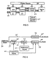
- the optical storage system is depicted in FIG 4 .
- the laser beams for the write/read/erase cycles are provided by a frequency doubled diode laser 16 operating at 488nm, a diode laser 17 operating at 780nm and a helium neon laser 18 operating at 633nm.
- the laser beams 19, 20 and 21 respectively are directed to the optical head 24 by mirrors 22 and 23.
- the optical head 24 performs all necessary beam processing to effect holographic data recording in the optical storage means 25.
- the operation of the optical head 24 is controlled by control means 26.
- a signal processor means 27 performs encoding of data to be written to the optical storage means 25 and decoding of signals received from the optical storage means by the optical head.
- the signal processor means 27 and control means 26 may conveniently be embodied in a personal computer.
- An alternative source of coherent radiation in the blue region is a Pr 3+ laser that emits at 490nm.
- the Pr 3+ laser can be very compact when provided as a Pr 3+ -doped fluoride fibre up-conversion laser.
- the up-conversion laser is pumped by two laser diodes operating at 1017nm and 835nm, both of which are available laser diodes.
- the Pr 3+ also has a relatively strong emission at 635nm which can be selected by appropriate control of the laser operation.
- the Pr 3+ laser can therefore provide the wavelengths for both writing and erasing.
- the 635nm beam could also be used for reading most materials although it is generally desirable to read at a different wavelength from the writing wavelength.
- a 780nm diode laser can be used for this purpose.
- the control means 26 controls the wavelength selection in the optical head 24 (described below) and operation of the lasers as required. To obtain necessary power densities the Pr 3+ laser is operated Q-switched and the control of this function is by the control means 26.
- the approximate power densities required and achievable are 5-10mW/cm 2 at 490nm for writing, 5mW/cm 2 at 780nm for reading and 10mW/cm2 at 635nm for erasing.
- erasure may be effected thermally or by an electric field. In these cases the application of the thermal or electric energy is controlled by the control means.
- the choice of optical, thermal or electric erasure is dependent on the storage medium of the optical storage means.
- Data is stored in the optical storage means in a series of diffraction (Airy) patterns.
- Conventional optical storage uses only binary signals.
- the inventors have found that higher order modes can be stored in the same data storage area as currently used. This is typically a spot 0.5 ⁇ m in diameter.
- the spots are arranged in tracks and these are typically arranged on 1 ⁇ m centres.
- the inventors have also found that a diffraction pattern can be recorded in the 0.5 ⁇ m spot providing the wavelength of the light is sufficiently short for two waves separated in phase to interfere.
- the inventors use a writing wavelength of 490nm.
- the optical storage means is illuminated by a reference beam and a writing beam separated in phase. The two beams interfere to produce interference fringes.
- the fringes contain both phase and amplitude information which is extracted by the reading beam.
- the reflected reading beam is detected and the intensity is measured.
- the intensity of the reflected beam varies essentially as the cosine of the phase difference between the reference beam and the writing beam.
- the intensity (the square of the amplitude)is essentially proportional to the phase difference between the beams.
- the signal from a simple detector such as a silicon photodiode can be used to differentiate between recorded interference patterns. This gives a digital range only limited by the grain resolution of the recording medium and the signal resolution of the detector. The inventors hypothesise that ten or more digits may be possible. Four digits is equivalent to two bits using binary recording, so the data storage capacity is doubled in the absence of other considerations.
- one diffraction spot will be equivalent to 1 byte of information.
- Each airy pattern will be picked up by a photodetector, and the intensity converted to the phase, and amplitude information recorded in each spot.
- the phase information would correspond to a particular 4 bit state, and the amplitude would correspond to a particular 4 bit state.
- the two states combined together would yield an 8 bit binary code which corresponds to one byte of information per dot.
- both the amplitude and phase information each can be broken down into 16 different intensity levels, with each level corresponding to a particular 4 bit binary code, when combined together produce one byte of information per dot.
- a Fraunhofer Diffraction pattern will contain the diffraction pattern within the designated spot area through the writing of Airy patterns.
- the light beam originates from a circular aperture, namely an optical fibre, rather than a slit.
- the basic principle is that of a Fraunhofer diffraction pattern, which represents the Fourier analysis of the diffracting aperture, in this case a grating or hologram.
- the diffraction pattern consists of an undeviated beam (the "dc" component) plus one order of diffraction on each side.
- the pattern is a superposition of two sine gratings.
- the optical storage means thus performs a Fourier synthesis when exposed, and adds together the individual sine waves caused by the interference between the reference and the writing beam.
- the result is a complex periodic wave pattern.
- the individual gratings can be encoded by modulating the phase, amplitude, and polarization of the writing beam, with respect to the reference beam. On reillumination at the reference beam angle, the encoded reading beam is returned and directed to a photodetector which detects the intensity change and decodes the object beam.
- the optical head may be an integrated optical device or a hybrid optomechanical device.
- the steering of the write, read and erase beams is achieved by acoustooptic or electrooptic beam deflectors.
- the structure of the integrated optical head is described in more detail below.
- the head is physically moved for the write, read and erase beams to access different storage addresses on the optical storage means.
- the optomechanical head is also described in more detail below.
- the control means comprises a power supply 28, which powers an optical head control board 29 for controlling the operation of the optical head 24.
- the optical head control board 29 will also control the servo mechanism 30 that moves the optical head 24 relative to the optical storage means 25.
- Data is received via an IDE board 31 that is also powered by the power supply 28. Data is moved from an external source through the IDE board 31 to the optical head control board 29 and hence the optical head 24 on databus 32.
- a control bus 33 is provided for control signals.
- the signal processor 27 analysis the signals read from the optical storage means 25.
- One scheme for effecting the signal processing (a simple detector) has been described above.
- a more efficient system is shown in FIG 6 .
- the process is essentially a heterodyne detection process .
- the reflected beam 34 is split with a portion 35 going to an amplitude detector 36 and a portion 37 going to a phase detector 38.
- the portion 37 is combined in a Bragg cell 39 with a frequency ramp 40.
- the combined optical signal 41 is mixed in a mixer 42 with a reference signal 43 and then goes to the detector 38 which also receives the frequency ramp 40.
- Heterodyne detection results in a phase signal 44 when the modulation frequency of the reflected beam equals that of the frequency of the ramp thus indicating that modulation frequency which is proportional to the phase difference.
- the detector 36 provides an amplitude signal 45 which directly indicates the amplitude of the reflected beam.
- An alternative signal processing technique is to use Fourier transforms.
- Fourier transform signal processing provides the phase directly rather than indirectly as in the method described above.
- Direct measurement of the phase difference between the reference and object beams provides double the data storage since the phase can vary between - ⁇ /2 to ⁇ /2 corresponding to a data range of -1 to 1, whereas the above signal processing based on measuring amplitude can only have a data range of 0 to 1.
- the data range is quantised to provide multiple digits.
- Amplitude Shift Keying, Phase Shift Keying, and Polarization Shift Keying can be employed for modulation and demodulation of the encoded beams.
- the signal processor means decodes the phase, amplitude, and polarization states through coherent heterodyne detection.
- Optical detection as shown in FIG 6 allows storage of phase and amplitude information which can be correlated with pre-stored data (eg. a holographic photo) hence allowing positive identification of a person by comparison of three dimensional data.
- pre-stored data eg. a holographic photo
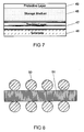
- the structure of the optical storage means is depicted in FIG 7 .
- the storage means comprises a base material 46 which is suitably a metallised Mylar sheet.
- the base material 46 is embossed with a tracking layer 47.
- the tracking layer 47 may suitably be a holographic layer incorporating the tracks.
- the layer is suitably 30 ⁇ m thick. This tracking layer 47 serves to assist in the tracking process and provides tracking information.
- An erasable storage medium 48 is coated over the tracking layer 47.
- the storage medium is typically 50 ⁇ m thick and able to store multiple diffraction patterns at varying depths.
- a clear protective outer layer 49 is then coated over the storage means to give durability.
- the tracking layer 47 provides all track, sector and alignment information required for tracking in the x-y plane.
- the tracks act as a virtual linear incremental optical encoder. Initially the optical head must be zeroed using zero reference marks for both the x & y coordinates. The control means may then keep track of which track or sector it is in via simple addition and subtraction of track and sector lines passed.
- the under face of the base material may have printed or embossed information as commonly found on existing credit cards.
- optical storage medium it is also necessary to add additional layers to facilitate erasure of data.
- an oxide layer is required for thermally erasable optical storage media.
- the optical storage means is commonly produced as a card about the size of a standard credit card.
- the first step in producing the card is to produce a master plate from which the card is embossed to form tracks.
- the card is formed as a metallised Mylar substrate on which the erasable storage medium is deposited.
- the master plate may be formed using an electronic or laser scribing process.
- the data density can be as great as 50000 lines/cm compared with 5000 lines/cm in current dot printed CD technology.
- the structure of the data dots 50 and tracking lines 51 is shown in FIG 8 .
- the data dots are 0.5 ⁇ m diameter on 1.0 ⁇ m centres with a 0.75 ⁇ m pitch.
- the tracking line has a width of 0.5 ⁇ m.
- each card only holds the raw tracks.
- the encoding occurs during the write process.
- the data capacity of the card is more than 250MB in a single layer without enhanced storage techniques.
- the data storage capacity of the optical storage card can be increased by recording data in multiple layers. Since a holographic recording is only reconstructed by illuminating at the original recording angle it is possible to make multiple recordings in the same spot by recording at different angles.
- the process is essentially the recording of multiple stack of thin film holograms. It is possible to record ten or more thin film holograms in the same diffraction spot.
- An optical data storage card can be used for storing digital information such as digitised photographs, pictures, information and digitised sound recordings. Uses will range from storing of digitised photographs, and related information for driver's licences as a fast and foolproof verification security device and associated hand held peripherals for police and nominated department of transport officials, to credit card and bank card security and verification applications, to a read/write card which can be inserted in place of a magnetic disk for storage purposes, to video card in place of existing video tapes.
- One suitable optical storage medium is a poly(methyl methacrylate) or poly(vinyl carbazole) polymer doped with fulgide E- ⁇ (2,5-dimethyl 3-furyl) ethylidene (adamantylidene)-succinic anhydride (an organic dye sold as Aberchrome 670). Fulgides are typically yellow or orange crystalline compounds. The colour in the polymer matrix can be changed to blue by irradiation with ultraviolet light so that the maximum absorption band is in the visible around 525nm. Data is stored in the medium holographically with a writing wavelength of 355nm which can be supplied by a frequency tripled diode-pumped Nd:YAG laser.
- the reading wavelength is outside the absorption band at 670nm, which can be provided by a diode laser.
- the recorded data is erased by absorption in the 525nm band of an erasing wavelength such as 532nm provided by a frequency doubled Nd:YAG laser or 633nm provided by a HeNe laser.
- the absorption profile of the fulgide in PVCz is shown in FIG 9 .
- the full line shows the absorption spectrum after writing with irradiation near 355nm and the dashed line shows the absorption spectrum after erasing with irradiation near 532nm.
- optical storage medium spiropyran-doped poly(vinyl carbazole).
- An optical storage medium of this material can be written at 355nm (frequency tripled diode-pumped Nd:YAG laser or frequency doubled diode laser), read at 488nm (frequency doubled diode) and erased at 633nm (He-Ne laser).
- the absorption profile of the material is shown in FIG 10 .
- the full line shows the absorption spectrum after writing with irradiation near 355nm and the dashed line shows the absorption spectrum after erasing with irradiation near 633nm.
- a further choice for optical storage medium is a photochromic dye dispersed in fulgide doped Polymethyl methacrylate, similar to the first example described above.
- the material when exposed to certain wavelengths, creates colour centres in the material. These colour centres have the ability to undergo many reversible transitions. These reversible transitions allow the material to be written to and erased with multiple exposures (up to 100,000 reversible cycles and more).
- the material is very stable and has no environmental constraints. The shelf life of the material is expected to be in excess of 20 years.
- the data is completely non recoverable after erasure, and the absorption band is completely broken down. There is also no possibility of bit migration due to the nature of the material.
- the percentage of dye dispersed in the PMMA can be varied to allow wavelength shifting to occur in order to selectively design the material to suit the wavelength characteristics of the laser.
- the material has a threshold energy level before erasure takes place and the data is affected.
- the erasing beam will not affect the prerecorded data when other layers are accessed via Bragg angle selection.
- the material requires a pre-exposure to a UV lamp/source before the material can be written to in the 490nm region.
- a fixed pre-exposure of the material to UV for a longer period may fix the material permanently and allow the material to be wavelength selective at all times.
- a typical angle separation between the reference and writing beams for this material is 20°.
- the optical head consists of an integrated optical element comprising a fibre-optic bundle that accesses multiple addressable spots on the storage means at any one time.
- the fibre-optic array is modulated and beam steered using electrooptic and acoustooptic modulators.
- a multiplexing array 52 converts the three input beams to one output beam that is wavelength switched in accordance with the write/read/erase cycle.
- a demultiplexer array 53 splits the output beam into a plurality of beams for launching into an integrated optical waveguide comprising a phase modulator 54, amplitude modulator 55 and polarization modulator 56. From the integrated optical waveguide the beams enter an electrooptic switching array 57 and are then collimated by a holographic optical element 58 and focused into an electrooptic or acoustooptic beam deflector 59 which directs the beams towards the optical storage means 25 at specific angles.
- the multiplexer 52 is shown in more detail in FIG 12 . It comprises one fibre-optic input 60a, 60b and 60c, per laser. The inputs are selectively switched to the output 61 by electrooptic switching elements 62 and 63.
- the output 61 becomes the input 64 to the demultiplexer 53 as shown in FIG 13 .
- the beam is demultiplexed into a number of beams for launching into phase modulator 54.
- the demultiplexer 53 has a similar structure to the multiplexer 52 with switching provided by electrooptic switching elements, such as 65.
- optical modulators are optical waveguide devices fabricated from silica glass or lithium niobate.
- the optical waveguide device that controls the amplitude and phase modulation is an interferometric intensity modulator, such as Mach-Zehnder type interferometer shown in detail in FIG 14 .
- the device comprises multiple modulator elements such as 66.
- Each element 66 comprises two Y-junctions, such as 67 and 68, that give an equal division of the input optical power. With no potential applied to the electrodes, the input optical power is split into the two arms at the Y-junction 67 and arrives at the second Y-junction 68 in phase giving an intensity maximum at the waveguide output 69.
- Such interferometric modulators have been demonstrated to operate at high speeds.
- a 1.1GHz modulation bandwidth has been reported for a 6 mm interferometer employing a 3.8 volt modulation depth across a 0.9 micrometer modulation gap.
- the polarization modulator 56 is shown in more detail in FIG 15 .
- the device comprises two elements 72a and 72b.
- Each element comprises a non-linear device 73, such as silica glass or X-cut lithium niobate.
- the longitudinal electrodes 74a and 74b are placed symmetrically over a Z-propagating waveguide diffused into the non-linear substrate. Voltages applied to the electrodes produce an electric field that can orientate the polarization of a propagating wave in any direction.
- This technique offers a robust, mechanically stable method of polarization control which has been demonstrated in both laboratory and field installed optical fibre systems, with no measurable sensitivity penalties.
- the polarization modulator 56 produces multi-level phase shift keying between TE and TM modes. These polarization states are then maintained during transmission within a single mode fibre.
- the modulator 56 has a transmission rate of 560 Mbits/sec.
- the electro-optic switching array 57 is shown in more detail in FIG 16 .
- the array 57 comprises a plurality of input fibres, such as 75, and a plurality of output fibres, such as 76.
- a matrix of electrooptic switching elements, such as 77, are arranged such that any input, or combination of inputs can be switched to any one or more outputs.
- the holographic optical element 58 is a combined collimator and focussing element that collects the output from the electrooptic switching array 57 and focuses into the beam deflector 59.
- the beam deflector 59 comprises an array of acoustooptic or electrooptic modulator elements.
- Each element comprises an acoustic transducer 79 in close contact with a transparent medium 80.
- the transducer 79 produces a travelling acoustic wave in the medium 80.
- the acoustic wave produces a periodic variation in density (ie mechanical strain) along its path which gives rise to a corresponding change in the refractive index within the medium due to the photoelastic effect.
- a moving optical phase diffraction grating is produced in the medium 80.
- a light beam passing through the medium 80 and crossing the path of the acoustic wave is Bragg diffracted by the phase grating from zero order into higher order modes.
- the deflected beams interfere in the optical storage means 25 to form individual diffraction patterns.
- the location of the diffraction patterns in the XY plane is determined by addressing different cells in the optical head 24.
- the Z axis is written to by writing at varying Bragg angles to the optical storage means 25, thus creating a series of 2D Fraunhoffer diffraction patterns stacked one on top of the other in the material.
- the data contained in each diffraction pattern is determined by the phase, amplitude and polarization settings in the optical head 24 as determined by the signal processor means 27.
- the diffraction patterns are read by addressing the recorded diffraction patterns across the XY plane and then in the Z plane and reconstructing the holograms.
- the encoded reading beam will be returned by the hologram and passes back through the optical head, to a detector which records the signal.
- the signal is analysed in the signal processor means 27 to obtain the phase, amplitude and polarization codes.
- the beam deflector 59 can be replaced by a servo device to form an optomechanical head.
- the optomechanical head is physically moved to access different regions of the optical storage means.
- the optomechanical head will operate in the same manner as the optical head except that it will physically move in the XY plane through a motor control system and a transducer coil mechanism which allows for high precision alignment during the tracking process.
- control means 26 addresses a tracking beam 81 that leads the optomechanical head 82 by an optimum coupling angle, as depicted in FIG 18 .
- the tracking layer 47 reflects the tracking beam 81 prior to the optomechanical head 82 actually reaching the sector headers. The reflected tracking beam is detected and allows a distance 'd' for the drive to prepare for a write, read or erase operation.
- the mechanical portion of the optomechanical head is a two stage servo device capable of achieving linear motions in 3 axis (x, y, and z) with a resolution of +100 nanometres and velocity of 2m/s or greater.
- a high precision zero backlash lead screw driven by a DC servomotor with high count rotary encoder is used for the first stage to position the optical head to within the span of the non-erasable guidance tracks mentioned above.
- the second stage is a micro positioner such as a peizo-electric (or voice coil) element or, alternatively, a high resolution lead screw drive, similar to the first stage, working in differential mode.
- the second stage centres the optical head relative to these tracks for accurate writing, reading or erasing.
- PVDF peizo-electric plastic
- PVDF peizo-electric plastic
- the entire system can be contained in a standard size drive that interfaces with a personal computer.
- a sketch of a suitable drive is shown at FIG 19 .
- the drive will recognise the drive as being similar in size and design to a compact disk drive or floppy disk drive.
- the optical storage system described herein is not reliant on complex optical arrangements such as CCD arrays and spatial light modulators to recompose a given data page. Rather, the system provides for simple, low cross-talk, low interference and high signal to noise ratio, as the diffraction patterns require limited image processing, and are easy to distinguish. Thus, the signal processing allows much greater processing speeds due to the simplicity of the conversion algorithms required. Appropriate signal processing algorithms would be well known to persons skilled in the art and determined by the particular encoding scheme employed.
- the system uses an integrated optical head requiring little or no moving parts. An alternative optomechanical head is also described.
- the optical head is composed of inexpensive fibres and waveguide structures which are designed for low cost mass production.
- the optical storage means is preferably the size of a credit card with a durable non-removable outer casing preventing surface degradation from dust, scratching, and general handling.
- the storage medium of the optical storage means is inexpensive to produce and allows for fast access times. It is capable of reading, writing, and erasing with very low power requirements.
- the lasers for the optical storage system are inexpensive, compact lasers with lower power requirements.
Landscapes
- Chemical & Material Sciences (AREA)
- Inorganic Chemistry (AREA)
- Engineering & Computer Science (AREA)
- Manufacturing & Machinery (AREA)
- Physics & Mathematics (AREA)
- Optics & Photonics (AREA)
- Optical Recording Or Reproduction (AREA)
- Holo Graphy (AREA)
Claims (30)
- Système d'enregistrement optique comprenant :- un moyen d'enregistrement optique (25) pour l'enregistrement holographique de données, ledit moyen d'enregistrement optique comprenant un support d'enregistrement inscriptible, lisible et effaçable ;- une première source (16) de rayonnement cohérent pour écrire lesdites données dans ledit moyen d'enregistrement optique ;- une deuxième source (17) de rayonnement cohérent pour lire lesdites données à partir dudit moyen d'enregistrement optique ;- des moyens pour effacer lesdites données dudit moyen d'enregistrement optique (25) ;- une tête optique (24) pour diriger ledit rayonnement cohérent et lesdits moyens d'effacement vers ledit moyen d'enregistrement optique ;- un moyen de commande (26) pour commander à la tête optique d'écrire, lire et effacer lesdites données ; et- des moyens de traitement de signaux (27) pour coder et décoder le rayonnement cohérent ;dans lequel- lesdites données sont enregistrées dans au moins un point d'enregistrement de données (50), lesdites données étant enregistrées sous la forme d'un diagramme de diffraction dans chacun desdits points d'enregistrement de données ; et- ladite tête optique (24) comprend des moyens (54, 55, 56) pour moduler une ou plusieurs caractéristiques parmi la phase, l'amplitude et la polarisation d'un faisceau émis par la première source de rayonnement cohérent, de sorte que des données à plusieurs binaires sont codées dans ledit diagramme de diffraction, lesdits moyens de traitement de signaux commandant lesdits moyens (54, 55, 56) de modulation.
- Système d'enregistrement optique selon la revendication 1, dans lequel la première source (16) de rayonnement cohérent pour l'écriture est un laser fonctionnant à une longueur d'onde bleue.
- Système d'enregistrement optique selon la revendication 1, dans lequel la deuxième source (17) de rayonnement cohérent pour la lecture est un laser fonctionnant à une longueur d'onde rouge.
- Système d'enregistrement optique selon la revendication 1, dans lequel le moyen d'effacement est une source thermique.
- Système d'enregistrement optique selon la revendication 1, dans lequel le moyen d'effacement est un champ électrique.
- Système d'enregistrement optique selon la revendication 1, dans lequel le moyen d'effacement est un laser fonctionnant à une longueur d'onde située dans une bande d'absorption du support d'enregistrement.
- Système d'enregistrement optique selon la revendication 1, dans lequel la tête optique comprend des moyens de détection échangeant des signaux avec lesdits moyens de traitement de signaux, de sorte que les moyens de traitement de signaux décodent les modulations détectées par les moyens de détection.
- Système d'enregistrement optique selon la revendication 1, comprenant en outre un moyen servomécanique pour réaliser un positionnement relatif de la tête optique par rapport au moyen d'enregistrement optique.
- Système d'enregistrement optique selon la revendication 1, dans lequel le moyen d'enregistrement optique comprend :- un substrat revêtu d'un matériau réfléchissant ;- une couche de suivi déposée sur le substrat, ladite couche de suivi comprenant une pluralité de pistes, chaque piste ayant une partie de suivi et une partie d'écriture de données ; et un support d'enregistrement effaçable déposé sur la couche de suivi, dans lequel les données sont enregistrées dans le support d'enregistrement effaçable sous la forme de diagrammes de diffraction.
- Système d'enregistrement optique selon la revendication 9, dans lequel le substrat est revêtu d'un matériau réfléchissant.
- Système d'enregistrement optique selon la revendication 9, dans lequel la couche de suivi est une couche en relief à surface gaufrée.
- Système d'enregistrement optique selon la revendication 9, dans lequel la partie de suivi de chaque piste est une bande linéaire et la partie d'écriture de données est une matrice de points.
- Système d'enregistrement optique selon la revendication 9, dans lequel les pistes sont divisées en une pluralité de secteurs et les secteurs sont divisés en un certain nombre de champs.
- Système d'enregistrement optique selon la revendication 9, dans lequel les champs comprennent un ou plusieurs champs choisis parmi un champ d'identification de secteur, un champ d'identification de données, un champ de contrôle et de correction d'erreur et un champ d'enregistrement de données.
- Système d'enregistrement optique selon la revendication 9, dans lequel le support d'enregistrement effaçable est un support épais permettant d'enregistrer plusieurs hologrammes sous plusieurs angles et à plusieurs profondeurs dans le support.
- Système d'enregistrement optique selon la revendication 9, dans lequel le support d'enregistrement effaçable est choisi parmi un matériau photoréfractif, un matériau polymère ou un matériau thermoplastique.
- Système d'enregistrement optique selon la revendication 9, dans lequel le support d'enregistrement effaçable est un matériau thermoplastique effaçable par l'application d'un champ thermique.
- Système d'enregistrement optique selon la revendication 9, dans lequel le support d'enregistrement effaçable est un matériau polymère photoréfractif effaçable par champ qui est effaçable par l'application d'un champ électrique puissant approprié pour réaligner les chaînes du polymère du support d'enregistrement.
- Système d'enregistrement optique selon la revendication 1, dans lequel la tête optique comprend :- des moyens multiplexeurs pour sélectionner une ou plusieurs sources de rayonnement cohérent ;- des moyens démultiplexeurs pour diviser le rayonnement sélectionné en multiples faisceaux ;- des moyens pour coder une modulation d'un ou plusieurs des multiples faisceaux ; et- des moyens pour dévier les multiples faisceaux modulés vers un emplacement souhaité dans un moyen d'enregistrement optique.
- Système d'enregistrement optique selon la revendication 19, dans lequel les moyens pour coder une modulation comprennent des moyens pour coder une modulation d'amplitude et/ou des moyens pour coder une modulation de phase et/ou des moyens pour coder une modulation de polarisation d'un ou plusieurs des multiples faisceaux.
- Système d'enregistrement optique selon la revendication 19, dans lequel les moyens pour dévier les multiples faisceaux modulés comprennent une pluralité de cellules de déviation et des moyens pour faire passer un ou plusieurs des multiples faisceaux modulés sur une cellule de déviation souhaitée.
- Système d'enregistrement optique selon la revendication 19, comprenant en outre des moyens pour recevoir un rayonnement réfléchi et diriger le rayonnement réfléchi vers un moyen de détection.
- Système d'enregistrement optique selon la revendication 22, dans lequel le moyen de détection détecte le codage de phase, d'amplitude et de polarisation.
- Système d'enregistrement optique selon la revendication 19, dans lequel le moyen pour coder une modulation d'amplitude et le moyen pour coder une modulation de phase sont un ou plusieurs interféromètres de Mach-Zehnder.
- Système d'enregistrement optique selon la revendication 19, dans lequel le moyen pour coder une modulation de polarisation est un dispositif de commande de polarisation électro-optique ou acousto-optique.
- Procédé d'enregistrement de données holographiques utilisant le système d'enregistrement optique selon la revendication 1, ledit procédé comprenant les étapes consistant à :- produire une plaque photographique contenant un négatif d'une pluralité de pistes ;- produire un moyen d'enregistrement optique vierge (25) qui est un substrat (46) revêtu d'une couche réfléchissante,le procédé étant caractérisé par les étapes supplémentaires consistant à :- gaufrer le moyen d'enregistrement optique vierge à partir de la plaque photographique pour former une pluralité de pistes dans une couche de suivi (47) ;- revêtir le moyen d'enregistrement optique gaufré d'un support d'enregistrement effaçable (48) ; et- écrire des données par voie holographique sur les pistes du moyen d'enregistrement optique, lesdites données étant enregistrées dans au moins un point d'enregistrement de données, lesdites données étant enregistrées sous la forme d'un diagramme de diffraction dans chacun desdits points d'enregistrement de données, et moduler une ou plusieurs caractéristiques parmi la phase, l'amplitude et la polarisation du faisceau d'écriture cohérent de sorte que des données à plusieurs binaires soient codées dans ledit diagramme de diffraction ;dans lequel les données sont lues par voie holographique par la mesure des signaux provenant du moyen d'enregistrement optique (25) lorsqu'il est illuminé par un faisceau de lecture cohérent (20).
- Procédé selon la revendication 26, dans lequel l'étape consistant à lire par voie holographique les données enregistrées dans le moyen d'enregistrement optique comprend l'étape consistant à illuminer le moyen d'enregistrement optique avec un faisceau de lecture ayant une longueur d'onde différente de celle du faisceau de référence et sous un angle différent de celui utilisé pour enregistrer les données.
- Procédé selon la revendication 26, dans lequel les données sont enregistrées dans une pluralité de zones, chaque zone correspondant à une profondeur différente dans les pistes du moyen d'enregistrement optique.
- Procédé selon la revendication 26, dans lequel les données sont protégées contre une lecture non autorisée par l'écriture des données dans les secteurs dans un ordre codé.
- Procédé selon la revendication 29, dans lequel le premier secteur enregistré est enregistré avec un code qui est lisible pour décoder l'ordre d'écriture.
Applications Claiming Priority (5)
| Application Number | Priority Date | Filing Date | Title |
|---|---|---|---|
| AUPN4010A AUPN401095A0 (en) | 1995-07-05 | 1995-07-05 | Optical storage means |
| AUPN4010/95 | 1995-07-05 | ||
| AUPN7629A AUPN762996A0 (en) | 1996-01-19 | 1996-01-19 | Optical head |
| AUPN7629/96 | 1996-01-19 | ||
| PCT/AU1996/000423 WO1997002563A1 (fr) | 1995-07-05 | 1996-07-05 | Systeme de memorisation optique |
Publications (3)
| Publication Number | Publication Date |
|---|---|
| EP0836738A1 EP0836738A1 (fr) | 1998-04-22 |
| EP0836738A4 EP0836738A4 (fr) | 1999-09-22 |
| EP0836738B1 true EP0836738B1 (fr) | 2008-08-27 |
Family
ID=25644989
Family Applications (1)
| Application Number | Title | Priority Date | Filing Date |
|---|---|---|---|
| EP96921826A Expired - Lifetime EP0836738B1 (fr) | 1995-07-05 | 1996-07-05 | Systeme de memorisation optique |
Country Status (7)
| Country | Link |
|---|---|
| US (1) | US6154432A (fr) |
| EP (1) | EP0836738B1 (fr) |
| JP (1) | JPH11508719A (fr) |
| KR (1) | KR19990028735A (fr) |
| CA (1) | CA2226268C (fr) |
| DE (1) | DE69637663D1 (fr) |
| WO (1) | WO1997002563A1 (fr) |
Families Citing this family (40)
| Publication number | Priority date | Publication date | Assignee | Title |
|---|---|---|---|---|
| DE19801470A1 (de) * | 1998-01-16 | 1999-07-22 | Thilo Weitzel | Vorrichtung und Verfahren zur optischen Aufnahme, Speicherung und Wiedergabe von Informationen |
| JP3729477B2 (ja) * | 1998-02-27 | 2005-12-21 | 秀嘉 堀米 | ホログラム作成装置および方法 |
| HU9801029D0 (en) * | 1998-05-05 | 1998-06-29 | Optilink Ab | Method and system for recording information on a holographic card |
| GB2341565A (en) * | 1998-09-18 | 2000-03-22 | Martin Processing Co Inc | Photosensitive films |
| HUP9802755A3 (en) * | 1998-11-27 | 2002-05-28 | Optilink Ab | Holographic chip and optical system for the holographic chip |
| US6450642B1 (en) * | 1999-01-12 | 2002-09-17 | California Institute Of Technology | Lenses capable of post-fabrication power modification |
| US6466528B1 (en) * | 1999-03-31 | 2002-10-15 | Cirrus Logic, Inc. | Flexible interface signal for use in an optical disk system and systems and methods using the same |
| US20030092788A1 (en) * | 1999-09-17 | 2003-05-15 | Tigran Galstian | Near infrared sensitive photopolymerizable composition |
| GB9929953D0 (en) * | 1999-12-17 | 2000-02-09 | Cambridge Res & Innovation | Holographic recording medium,and method of forming thereof,utilizing linearly polarized light |
| US6749632B2 (en) | 2000-03-20 | 2004-06-15 | California Institute Of Technology | Application of wavefront sensor to lenses capable of post-fabrication power modification |
| DE10039374A1 (de) * | 2000-08-11 | 2002-02-21 | Eml Europ Media Lab Gmbh | Holographischer Datenspeicher |
| DE10039372C2 (de) * | 2000-08-11 | 2003-05-15 | Tesa Scribos Gmbh | Holographischer Datenspeicher |
| DE10053264A1 (de) * | 2000-10-26 | 2002-05-08 | Orga Kartensysteme Gmbh | Verfahren zum Einschreiben von Daten auf/in Datenträger mittels Laserstrahlung und damit hergestellte Datenträger |
| US6999397B2 (en) * | 2001-03-23 | 2006-02-14 | Daewoo Electronics Corp. | Holographic digital data storage system compatible with holographic and reflective medium |
| DE10122341A1 (de) * | 2001-05-09 | 2002-11-14 | Orga Kartensysteme Gmbh | Verfahren zur Herstellung eines Datenträgers mit holographischem Speicher zur schnellen Datenspeicherung |
| DE10128902A1 (de) | 2001-06-15 | 2003-10-16 | Tesa Scribos Gmbh | Holographischer Datenspeicher |
| US6780546B2 (en) | 2001-08-30 | 2004-08-24 | Inphase Technologies, Inc. | Blue-sensitized holographic media |
| GB2379441A (en) * | 2001-09-07 | 2003-03-12 | Polight Tech Ltd | Holographic recording medium |
| US20030064293A1 (en) * | 2001-09-07 | 2003-04-03 | Polight Technologies Ltd. | Holographic recording medium |
| KR100402397B1 (ko) * | 2001-09-28 | 2003-10-17 | (주)프리즘테크 | 홀로그램을 이용한 보안 카드의 제조방법 및 이 보안카드의 인증시스템 |
| US6888785B2 (en) | 2002-01-25 | 2005-05-03 | Sun Microsystems, Inc. | Fault tolerance mechanism for a storage device that stores data in stacks within an integral storage medium |
| US7115305B2 (en) * | 2002-02-01 | 2006-10-03 | California Institute Of Technology | Method of producing regular arrays of nano-scale objects using nano-structured block-copolymeric materials |
| JP2003233925A (ja) * | 2002-02-06 | 2003-08-22 | Pioneer Electronic Corp | 光集積デバイスおよび波長変動キャンセル方法 |
| CN1317452C (zh) * | 2002-05-08 | 2007-05-23 | 雷恩哈德库兹有限公司 | 带有激光敏感层的多层体 |
| GB0322031D0 (en) * | 2003-09-19 | 2003-10-22 | Optaglio Ltd | Optically variable diffractive device and related apparatus and method of reading |
| JP2005196826A (ja) * | 2003-12-26 | 2005-07-21 | Samsung Electronics Co Ltd | ホログラムメモリ用媒体 |
| JP4665404B2 (ja) * | 2004-02-16 | 2011-04-06 | 富士ゼロックス株式会社 | シュレッダ装置及びシュレッダ処理方法 |
| US7491628B2 (en) * | 2004-05-05 | 2009-02-17 | California Institute Of Technology | Method for patterning large scale nano-fibrous surfaces using capillography |
| US20050250046A1 (en) * | 2004-05-07 | 2005-11-10 | Samsung Electronics Co., Ltd. | Hologram recording medium and apparatus for and method of recording data on the recording medium |
| US8021967B2 (en) * | 2004-11-01 | 2011-09-20 | California Institute Of Technology | Nanoscale wicking methods and devices |
| JP4590635B2 (ja) * | 2005-04-28 | 2010-12-01 | 新オプトウエア株式会社 | 光情報再生方法、光情報再生装置、光情報記録再生方法及び光情報記録再生装置 |
| EP1845523A1 (fr) * | 2006-04-13 | 2007-10-17 | Deutsche Thomson-Brandt Gmbh | Méthode de compensation de la désadaptation de la longueur d'onde dans un système de stockage holographique |
| EP1933310A1 (fr) * | 2006-12-13 | 2008-06-18 | Deutsche Thomson OHG | Pré-exposition et durcissement d'un matériau photosensible pour le stockage de données optique |
| EP1933311B1 (fr) * | 2006-12-13 | 2010-06-02 | Thomson Licensing | Pré-exposition et séchage de matériau photosensible pour stockage de données optiques |
| US8180950B2 (en) * | 2007-06-15 | 2012-05-15 | International Business Machines Corporation | Apparatus and method to manage information using an optical and holographic data storage medium |
| US8045246B2 (en) * | 2009-06-18 | 2011-10-25 | Access Optical Networks, Inc. | Method and apparatus for bulk erasure in a holographic storage system |
| JP5358530B2 (ja) * | 2010-07-28 | 2013-12-04 | 日立コンシューマエレクトロニクス株式会社 | 光情報記録再生装置及び再生装置 |
| US9997189B2 (en) * | 2016-11-07 | 2018-06-12 | Seagate Technology Llc | Three dimensional electric field data storage device utilizing shockwaves and a light source |
| US10056146B2 (en) | 2016-11-07 | 2018-08-21 | Seagate Technology Llc | Electric field storage device |
| US11415822B2 (en) * | 2018-02-13 | 2022-08-16 | California Institute Of Technology | Capacitive modulators for high-efficiency electro-optical systems |
Citations (2)
| Publication number | Priority date | Publication date | Assignee | Title |
|---|---|---|---|---|
| US4655542A (en) * | 1985-05-06 | 1987-04-07 | International Business Machines Corporation | Optical signal processing arrangements |
| US5038335A (en) * | 1986-12-01 | 1991-08-06 | Miller William P | Hierarchically multiplexed optical recording system for storage of digital data |
Family Cites Families (21)
| Publication number | Priority date | Publication date | Assignee | Title |
|---|---|---|---|---|
| DE2203246C3 (de) * | 1972-01-24 | 1974-06-06 | Siemens Ag, 1000 Berlin Und 8000 Muenchen | Verfahren zur sequentiellen holografischen Vielkanalaufzeichnung analoger oder digitaler Daten auf einem Speicherband |
| US3976354A (en) * | 1973-12-14 | 1976-08-24 | Honeywell Inc. | Holographic memory with moving memory medium |
| US4295162A (en) * | 1975-09-11 | 1981-10-13 | Gte Laboratories Incorporated | Reading one-dimensional line image holograms of a video from a disc with a guide track |
| US3990773A (en) * | 1975-11-17 | 1976-11-09 | Rca Corporation | Binary-coded Fraunhofer hologram recording technique |
| DE3603268A1 (de) * | 1986-02-04 | 1987-09-24 | Roehm Gmbh | Verfahren zur reversiblen, optischen datenspeicherung (iii) |
| US4924199A (en) * | 1986-05-23 | 1990-05-08 | Olympus Optical Co., Ltd. | Optical card for data storage for use in a data recording and retrieving apparatus |
| JPS6347139A (ja) * | 1986-08-18 | 1988-02-27 | 帝人化成株式会社 | 樹脂積層板 |
| US4737745A (en) * | 1986-11-03 | 1988-04-12 | Westinghouse Electric Corp. | Electromagnetic interference filter assembly |
| US5319629A (en) * | 1988-08-25 | 1994-06-07 | Sparta, Inc. | Content addressable optical data storage system |
| US4910147A (en) * | 1988-09-21 | 1990-03-20 | Baxter International Inc. | Cell culture media flexible container |
| US5039583A (en) * | 1989-02-02 | 1991-08-13 | Ohio State University Research Foundation | Erasable optical information storage system |
| US5148421A (en) * | 1990-04-20 | 1992-09-15 | Matsushita Electric Industrial Co., Ltd. | Optical head |
| EP0483388B1 (fr) * | 1990-10-20 | 1993-08-18 | Ibm Deutschland Gmbh | Mémoire optique à accès aléatoire |
| JPH06509429A (ja) * | 1991-07-26 | 1994-10-20 | アキュウェーブ コーポレーション | 光屈折性システムおよび方法 |
| CA2079620A1 (fr) * | 1991-10-25 | 1993-04-26 | Roeland M. T. Hekker | Elements holographiques pour systeme d'enregistrement optique |
| US5195152A (en) * | 1991-11-04 | 1993-03-16 | Eastman Kodak Company | Multichannel optical recording apparatus employing laser diodes |
| DE4139563A1 (de) * | 1991-11-30 | 1993-06-03 | Roehm Gmbh | Reversibel vernetzte, orientierbare fluessigkristalline polymere |
| US5289454A (en) * | 1991-12-19 | 1994-02-22 | Minnesota Mining And Manufacturing Company | Optical disc addressing devices a method of use thereof |
| DE4208328C2 (de) * | 1992-03-16 | 2002-11-14 | Bayer Ag | Verfahren und Vorrichtung zur löschbaren Speicherung von Information |
| FR2703815B1 (fr) * | 1993-04-06 | 1995-06-30 | Imagine Technologies | Support portatif d'informations à mémoire holographique multiplexée. |
| US5978112A (en) * | 1995-02-15 | 1999-11-02 | California Institute Of Technology | Non-volatile readout of shift multiplexed holograms |
-
1996
- 1996-07-05 US US08/981,951 patent/US6154432A/en not_active Expired - Fee Related
- 1996-07-05 EP EP96921826A patent/EP0836738B1/fr not_active Expired - Lifetime
- 1996-07-05 DE DE69637663T patent/DE69637663D1/de not_active Expired - Fee Related
- 1996-07-05 KR KR1019980700033A patent/KR19990028735A/ko not_active Application Discontinuation
- 1996-07-05 WO PCT/AU1996/000423 patent/WO1997002563A1/fr active IP Right Grant
- 1996-07-05 CA CA002226268A patent/CA2226268C/fr not_active Expired - Fee Related
- 1996-07-05 JP JP9504658A patent/JPH11508719A/ja active Pending
Patent Citations (2)
| Publication number | Priority date | Publication date | Assignee | Title |
|---|---|---|---|---|
| US4655542A (en) * | 1985-05-06 | 1987-04-07 | International Business Machines Corporation | Optical signal processing arrangements |
| US5038335A (en) * | 1986-12-01 | 1991-08-06 | Miller William P | Hierarchically multiplexed optical recording system for storage of digital data |
Non-Patent Citations (2)
| Title |
|---|
| HEANUE J.F. ET AL: "Volume holographic storage and retrieval of digital information", CLEO, vol. CONF. 15, 1995, NEW YORK, IEEE, US, pages 27, XP001172954 * |
| YU V. ET AL: "Method for Multichannel Recording of Binary Data on Optical Disk", OPTOELECTRONICS, INSTRUMENTATION AND DATA PROCESSING (AVTOMETRIYA), no. 2, 1989, pages 77 - 87, XP008026434 * |
Also Published As
| Publication number | Publication date |
|---|---|
| US6154432A (en) | 2000-11-28 |
| WO1997002563A1 (fr) | 1997-01-23 |
| EP0836738A1 (fr) | 1998-04-22 |
| JPH11508719A (ja) | 1999-07-27 |
| CA2226268C (fr) | 2006-11-21 |
| KR19990028735A (ko) | 1999-04-15 |
| DE69637663D1 (de) | 2008-10-09 |
| EP0836738A4 (fr) | 1999-09-22 |
| CA2226268A1 (fr) | 1997-01-23 |
Similar Documents
| Publication | Publication Date | Title |
|---|---|---|
| EP0836738B1 (fr) | Systeme de memorisation optique | |
| EP1254398B1 (fr) | Procede et systeme d'enregistrement d'informations sur un support holographique | |
| EP0834174B1 (fr) | Support de memoire optique et procedes d'ecriture et de lecture | |
| US5373500A (en) | Optical readable carrier with diffractive tracks containing information bearing irregularity | |
| US5659536A (en) | Optical storage method and device for storing and reading digital information | |
| US6909684B2 (en) | Optical recording medium, holographic recording and/or retrieval method and holographic recording and/or retrieval apparatus | |
| US6556531B1 (en) | Multi-layered holographic read-only memory and data retrieval method | |
| KR20100074079A (ko) | 데이터 저장 장치 및 데이터 저장 방법 | |
| JP4342311B2 (ja) | 導波路多層ホログラフィックデータストレージ | |
| DE19534501C2 (de) | Optischer Datenspeicher hoher Dichte durch holographisches Multiplexing von Reflexionshologrammen in einer Schicht | |
| AU701056B2 (en) | Optical storage system | |
| JP2005078691A (ja) | ホログラフィック記録媒体 | |
| US20040190095A1 (en) | Optical recording medium and optical recording method | |
| JP2006259271A (ja) | ホログラム記録媒体及び記録方法 | |
| CN100507760C (zh) | 快速复制衍射存储器以大量生产 | |
| US20030147327A1 (en) | Holographic storage device with faceted surface structures and associated angle multiplexing method | |
| EP1837871B1 (fr) | Système et méthode de stockage de données holographique | |
| JP2013541797A (ja) | データ記録及び読出 | |
| Gaylord et al. | Application Areas | |
| JPH0461039A (ja) | 光記録媒体及びその記録再生方法 |
Legal Events
| Date | Code | Title | Description |
|---|---|---|---|
| PUAI | Public reference made under article 153(3) epc to a published international application that has entered the european phase |
Free format text: ORIGINAL CODE: 0009012 |
|
| 17P | Request for examination filed |
Effective date: 19980205 |
|
| AK | Designated contracting states |
Kind code of ref document: A1 Designated state(s): DE FR GB IT NL |
|
| A4 | Supplementary search report drawn up and despatched |
Effective date: 19990805 |
|
| AK | Designated contracting states |
Kind code of ref document: A4 Designated state(s): DE FR GB IT NL |
|
| RIC1 | Information provided on ipc code assigned before grant |
Free format text: 6G 11B 7/00 A, 6G 11B 7/12 B, 6G 11B 7/14 B, 6G 06K 19/16 B |
|
| 17Q | First examination report despatched |
Effective date: 20010719 |
|
| RIC1 | Information provided on ipc code assigned before grant |
Ipc: G06K 19/16 20060101ALI20070918BHEP Ipc: G11B 7/14 20060101ALI20070918BHEP Ipc: G11B 7/12 20060101ALI20070918BHEP Ipc: G11B 7/0065 20060101AFI20070918BHEP |
|
| GRAP | Despatch of communication of intention to grant a patent |
Free format text: ORIGINAL CODE: EPIDOSNIGR1 |
|
| GRAS | Grant fee paid |
Free format text: ORIGINAL CODE: EPIDOSNIGR3 |
|
| GRAA | (expected) grant |
Free format text: ORIGINAL CODE: 0009210 |
|
| AK | Designated contracting states |
Kind code of ref document: B1 Designated state(s): DE FR GB IT NL |
|
| REG | Reference to a national code |
Ref country code: GB Ref legal event code: FG4D |
|
| REF | Corresponds to: |
Ref document number: 69637663 Country of ref document: DE Date of ref document: 20081009 Kind code of ref document: P |
|
| PG25 | Lapsed in a contracting state [announced via postgrant information from national office to epo] |
Ref country code: NL Free format text: LAPSE BECAUSE OF FAILURE TO SUBMIT A TRANSLATION OF THE DESCRIPTION OR TO PAY THE FEE WITHIN THE PRESCRIBED TIME-LIMIT Effective date: 20080827 |
|
| PLBE | No opposition filed within time limit |
Free format text: ORIGINAL CODE: 0009261 |
|
| STAA | Information on the status of an ep patent application or granted ep patent |
Free format text: STATUS: NO OPPOSITION FILED WITHIN TIME LIMIT |
|
| 26N | No opposition filed |
Effective date: 20090528 |
|
| PG25 | Lapsed in a contracting state [announced via postgrant information from national office to epo] |
Ref country code: IT Free format text: LAPSE BECAUSE OF FAILURE TO SUBMIT A TRANSLATION OF THE DESCRIPTION OR TO PAY THE FEE WITHIN THE PRESCRIBED TIME-LIMIT Effective date: 20080827 |
|
| REG | Reference to a national code |
Ref country code: FR Ref legal event code: ST Effective date: 20100331 |
|
| PG25 | Lapsed in a contracting state [announced via postgrant information from national office to epo] |
Ref country code: FR Free format text: LAPSE BECAUSE OF NON-PAYMENT OF DUE FEES Effective date: 20090731 |
|
| PG25 | Lapsed in a contracting state [announced via postgrant information from national office to epo] |
Ref country code: DE Free format text: LAPSE BECAUSE OF NON-PAYMENT OF DUE FEES Effective date: 20100202 |
|
| PGFP | Annual fee paid to national office [announced via postgrant information from national office to epo] |
Ref country code: GB Payment date: 20100720 Year of fee payment: 15 |
|
| GBPC | Gb: european patent ceased through non-payment of renewal fee |
Effective date: 20110705 |
|
| PG25 | Lapsed in a contracting state [announced via postgrant information from national office to epo] |
Ref country code: GB Free format text: LAPSE BECAUSE OF NON-PAYMENT OF DUE FEES Effective date: 20110705 |