EP0835336B2 - A device and a method for epitaxially growing objects by cvd - Google Patents
A device and a method for epitaxially growing objects by cvd Download PDFInfo
- Publication number
- EP0835336B2 EP0835336B2 EP96922326A EP96922326A EP0835336B2 EP 0835336 B2 EP0835336 B2 EP 0835336B2 EP 96922326 A EP96922326 A EP 96922326A EP 96922326 A EP96922326 A EP 96922326A EP 0835336 B2 EP0835336 B2 EP 0835336B2
- Authority
- EP
- European Patent Office
- Prior art keywords
- substrate
- susceptor
- gas
- etching
- gas mixture
- Prior art date
- Legal status (The legal status is an assumption and is not a legal conclusion. Google has not performed a legal analysis and makes no representation as to the accuracy of the status listed.)
- Expired - Lifetime
Links
Images

Classifications
-
- C—CHEMISTRY; METALLURGY
- C30—CRYSTAL GROWTH
- C30B—SINGLE-CRYSTAL GROWTH; UNIDIRECTIONAL SOLIDIFICATION OF EUTECTIC MATERIAL OR UNIDIRECTIONAL DEMIXING OF EUTECTOID MATERIAL; REFINING BY ZONE-MELTING OF MATERIAL; PRODUCTION OF A HOMOGENEOUS POLYCRYSTALLINE MATERIAL WITH DEFINED STRUCTURE; SINGLE CRYSTALS OR HOMOGENEOUS POLYCRYSTALLINE MATERIAL WITH DEFINED STRUCTURE; AFTER-TREATMENT OF SINGLE CRYSTALS OR A HOMOGENEOUS POLYCRYSTALLINE MATERIAL WITH DEFINED STRUCTURE; APPARATUS THEREFOR
- C30B25/00—Single-crystal growth by chemical reaction of reactive gases, e.g. chemical vapour-deposition growth
- C30B25/02—Epitaxial-layer growth
-
- C—CHEMISTRY; METALLURGY
- C30—CRYSTAL GROWTH
- C30B—SINGLE-CRYSTAL GROWTH; UNIDIRECTIONAL SOLIDIFICATION OF EUTECTIC MATERIAL OR UNIDIRECTIONAL DEMIXING OF EUTECTOID MATERIAL; REFINING BY ZONE-MELTING OF MATERIAL; PRODUCTION OF A HOMOGENEOUS POLYCRYSTALLINE MATERIAL WITH DEFINED STRUCTURE; SINGLE CRYSTALS OR HOMOGENEOUS POLYCRYSTALLINE MATERIAL WITH DEFINED STRUCTURE; AFTER-TREATMENT OF SINGLE CRYSTALS OR A HOMOGENEOUS POLYCRYSTALLINE MATERIAL WITH DEFINED STRUCTURE; APPARATUS THEREFOR
- C30B29/00—Single crystals or homogeneous polycrystalline material with defined structure characterised by the material or by their shape
- C30B29/10—Inorganic compounds or compositions
- C30B29/36—Carbides
-
- C—CHEMISTRY; METALLURGY
- C30—CRYSTAL GROWTH
- C30B—SINGLE-CRYSTAL GROWTH; UNIDIRECTIONAL SOLIDIFICATION OF EUTECTIC MATERIAL OR UNIDIRECTIONAL DEMIXING OF EUTECTOID MATERIAL; REFINING BY ZONE-MELTING OF MATERIAL; PRODUCTION OF A HOMOGENEOUS POLYCRYSTALLINE MATERIAL WITH DEFINED STRUCTURE; SINGLE CRYSTALS OR HOMOGENEOUS POLYCRYSTALLINE MATERIAL WITH DEFINED STRUCTURE; AFTER-TREATMENT OF SINGLE CRYSTALS OR A HOMOGENEOUS POLYCRYSTALLINE MATERIAL WITH DEFINED STRUCTURE; APPARATUS THEREFOR
- C30B29/00—Single crystals or homogeneous polycrystalline material with defined structure characterised by the material or by their shape
- C30B29/10—Inorganic compounds or compositions
- C30B29/38—Nitrides
Definitions
- the present invention relates to a device for epitaxially growing layers of SiC by Chemical Vapour Deposition on a substrate comprising a susceptor having a circumferential wall surrounding a room for receiving the substrate and means for heating said circumferential susceptor walls and thereby the substrate and a gas mixture fed to the substrate for the growth by feeding means as well as a method for epitaxially growing objects by Chemical Vapour Deposition on a substrate according to the preamble of the first appended independent method claim.
- the invention is applicable to the growth of SiC and the problem of growing objects of a high crystalline quality and at a reasonable grow rate from the commercial point of view.
- SiC single crystals are in particular grown for being used in different types of semiconductor devices, such as for examples different types of diodes, transistors and thyristors, which are intended for applications in which it is possible to benefit from the superior properties of SiC in comparison with especially Si, namely the capability of SiC to function well under extreme conditions.
- the large band gap between the valence band and the conduction band of SiC makes devices fabricated from said material able to operate at high temperatures, namely up to 1000 K.
- high temperatures are needed for obtaining a good ordered growth thereof.
- the epitaxial growth of silicon carbide by Chemical Vapour Disposition is therefor carried out in a temperature regime of 1400-1700°C. These high temperatures are needed both to obtain decomposition by cracking of the Si- and C-containing precursor gases of said gas mixture and to ensure that the atoms are deposited on the substrate surface in an ordered manner.
- high temperatures also mean problems with impurities coming out of different types of material, so that the temperature could until now not be raised above said temperature interval, which results in such a low grow rate (some ⁇ m per hour) that it is out of the question to grow boules for forming i.a. substrates by using CVD, so that this method is only used for growing objects in the form of layers.
- the minority carrier lifetime is also reduced by the introduction of unwanted compensating acceptors in the N-type layer grown, so that a minority carrier lifetime acceptable for high-power bipolar devices could not be obtained until now. It is therefore important to produce layers of a high crystalline perfection at high grow rates without the introduction of compensating acceptors. Common impurities as nitrogen and oxygen may also be incorporated at lower concentrations at higher growth rates which also may influence the minority carrier lifetime positively.
- the seeded sublimation technique is presently used for growing boules, which may then be sliced to substrates.
- the crystalline quality of the boules grown by this technique is low in comparison with that of the SiC layers epitaxially grown by CVD.
- the substrates produced in this way are perforated by small holes called micropipes or pinholes, which limit the device area considerably which consequently make high-power devices of SiC not commercially interesting yet.
- the source is a SiC powder that sublimes, whereupon the gas species are transported by a temperature gradient to the seed crystal where the growth occurs.
- the conditions in the gas phase are governed by thermodynamics only, which makes it difficult to keep the C/Si ratio constant due to Si vapour leakage out of the system. Furthermore, the purity of the gases used for Chemical Vapour Deposition are several orders of magnitude higher than that of the source material used for seeded sublimation growth.
- the object of the present invention is to advise a solution to the problems discussed above by providing a device and a method making it possible to epitaxially grow layers/objects by Chemical Vapour Deposition at a high grow rate while still obtaining a high crystalline quality of the object grown.
- the present invention is based on the idea of carrying out the Chemical Vapour Deposition at such a high temperature that a continuous sublimation of material from the substrate takes place, and this is combined with an etching of the substrate through said at least one etching gas in the gas mixture and a deposition of elements resulting from decomposition of the precursor gases.
- This is a totally new way of carrying out epitaxial growth by Chemical Vapour Deposition and involves excellent results.
- the growth rate may be increased considerably with respect to the conventional Chemical Vapour Deposition technique and the crystalline quality of the material grown may at the same time be maintained or even improved.
- reaction zone and the sublimation zone into one single room, where the precursors are first decomposed, heated and then deposited on the substrate, there is no need to provide any substantial pressure difference between the inlet and the growth zone.
- susceptor the room
- the grow rates may be increased by 2-3 orders of magnitude compared to the conventional CVD technique, so that high quality layers may be produced at rates being commercially interesting.
- the etching by hydrogen or other etching gases of the object grown on said substrate is increased considerably at these higher temperatures, and it has been found that polycrystalline regions, i.e. regions with a lower quality, are more rapidly etched than monocrystalline regions, i.e. regions with a high quality, which results in a higher quality of the crystal grown.
- the grow rates obtained by the temperature increase according to the invention are high enough for making it very interesting to grow boules by the CVD technique.
- a gas mixture normally used in the CVD technique which means a purity of the components used for said growth of several orders of magnitude higher than the source material used for seeded sublimation growth.
- the degree of supersaturation which influences both the grow rate and the formation of micropipes can be varied, without any thermal gradient.
- boules having a superior crystalline quality to that obtained by using the seeded sublimation technique may be obtained at commercially interesting grow rates through the High Temperature Chemical Vapour Deposition (HTCVD) according to the invention.
- HTCVD High Temperature Chemical Vapour Deposition
- EP-A-0 554 047 describes a device and a method in which the growth of the single crystal on the seed crystal is obtained by using the seeded sublimation technique in the sublimation zone. Accordingly, solid-phase SiC particles formed in a reaction zone 20 are introduced into the sublimation zone and sublimated and transported to the growth zone through a thermal gradient and deposited on the seed crystal. This is, accordingly, a method being totally different from the method according to the present invention, since there is no combination of sublimation from the substrate, etching of the substrate and deposition of elements for the growth on the substrate as taught by the present invention.
- said circumferential walls of the device form a substantially cylindrical susceptor. It has turned out that this shape of the susceptor will be particularly advantageous for easily obtaining a uniform temperature over the entire susceptor wall while avoiding hot spots.
- the inner walls of the susceptor are made of or covered by a plate made of SiC, an alloy of SiC and the material grown or the material grown.
- a plate made of SiC, an alloy of SiC and the material grown or the material grown.
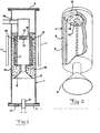
- Fig 1 shows schematically a device according to a preferred embodiment of the invention for epitaxially growing SiC by Chemical Vapour Deposition on a SiC-substrate in a simplified manner, and it is obvious that the device in question also comprises other means, such as pumps, but conventional equipment having nothing to do with the invention has been omitted for the sake of clearness and concentration to the inventional characteristics.
- the device comprises a vacuum casing 1 constituted by a tube 2 of quartz extending substantially vertically and two opposite end flanges 3 and 4.
- the end flange 4 is preferably removable so as to get access to the interior of the tube 2.
- a conduit 5 for supplying a stream of a gas mixture intended for the growth of a crystal is introduced through the lower end flange 3.
- the conduit 5 is connected to separate conduits leading to sources for the respective components of said gas mixture and these conduits are provided with flow regulating means not shown for regulating the content of each component in said gas mixture as desired.
- the device comprises a funnel 6 for concentrating the gas flow from the conduit 5 into a susceptor 7 (see also Fig 2 ).
- the susceptor 7 shown in Figs 1 and 2 is adapted for epitaxially growing layers of SiC.
- the susceptor is substantially cylindrical with circumferential walls 8 of a substantially uniform thickness.
- the walls are made of graphite, but they are internally coated by a layer of SiC 9 or alternatively covered by a cylindrical plate made of SiC.
- the space surrounding the susceptor is enclosed and filled by graphite foam 10 for thermal insulation for protecting the surrounding quartz tube 2.
- Rf-field radiating means 11 in the form of a Rf-coil surrounds the tube 2 along the longitudinal extension of the susceptor 7. This heating means 11 is arranged to radiate a Rf-field uniformly heating the walls 8 of the susceptor and thereby the gas mixture introduced into the susceptor.
- the susceptor 7 comprises a lid 12 of the same material as the rest of the susceptor, on the lower side of which a SiC substrate 13 is arranged and which may be removed from the rest of the susceptor so as to remove the substrate after a layer has been grown thereon.
- the lid 12 is provided with peripheral gas outlet holes 14, so that a preferable laminar gas flow will enter the susceptor room 18 through the lower inlet 15 and flow close to the substrate and leave the susceptor through the upper outlets 14 and then the device through a conduit 16 connected to a pump not shown.
- the temperature inside the susceptor 7 may be checked pyrometrically through looking into the susceptor 7 through a window indicated at 17.
- the function of the device is as follows: a gas mixture including Si- and C-containing precursor gases and one or more carrier gases is led through the conduit 5 in the direction of the susceptor inlet 15.
- the Si- containing precursor gas is preferably silane, while the C-containing precursor gas is propane or eventually methane.
- the carrier gas may be H 2 , but there may also be a content of a non-etching carrier gas, such as Ar, for a purpose which will be explained below.
- the heating means 11 will heat the susceptor walls uniformly to a temperature of about 2200°C, which is possible thanks to the substantially uniform thickness thereof resulting in no so called hot spots of the susceptor walls.
- the precursor gases entering the susceptor 7 will be heated through the susceptor and cracked into Si- and C-atoms, which will be transported to the substrate 13 and deposited thereon for epitaxially growing layers of SiC thereon. Thanks to the vertical arrangement of the susceptor walls the flow upwards of the hot gases heated will be promoted, so that the gases will be better utilized for the growth.
- the high temperature will lead to a continuous sublimation of SiC from the substrate as well as a considerable etching of the substrate through the etching carrier gas component (H 2 ), but the supply rate of the precursor gases and the carrier gas or gases is regulated so that a positive growth takes place, i.e.
- the deposition rate of elements forming the SiC layers grown on the substrate is higher than the rate of material leaving the layers on the substrate due to sublimation and etching.
- This interaction of deposition on one hand and etching and sublimation on the other for said growth promotes the formation of a crystal with a high crystalline quality, especially since the etching of polycrystalline regions is faster than that of monocrystalline regions.
- an increase of the content of a non-etching carrier gas with a reduction of the content of an etching carrier gas in the gas mixture while raising the temperature will give rise to an etching being below a critical level even at the high temperatures used. This means that the walls of the susceptor may be spared in spite of the high temperatures prevailing.
- Ar may be used as non-etching carrier gas and H 2 as etching carrier gas.
- the initial stage of the growth is particularly important for the quality of the layers grown also thereafter.
- the grow rate may therefore be kept low at the initial stage of growth to form a smooth uniform layer after which the grow rate gradually can be increased to 100 ⁇ m - several millimetres/hour depending on the temperature.
- SiC layers may in this way be grown at a high grow rate, possibly from 100 ⁇ m to a few millimetres per hour, on the substrate 13, and this high grow rate with said continuous sublimation and etching will give rise to a high quality of the layer grown in spite of the high temperatures, and due to the higher crystalline quality obtained at these temperature and due to a faster healing of crystalline imperfections propagating from the substrate the introduction of unwanted compensating acceptors into the layers grown is dramatically reduced with respect to the epitaxial growth of such layers by CVD at normal temperatures resulting in a significant prolongation of the minority carrier lifetime in the crystals grown. This is a vital improvement for the production of high-power bipolar devices.
- Fig 3 shows a further susceptor 7', which is adapted for growing boules 19 of SiC on a substrate in the form of a seed crystal indicated at 13'.
- This susceptor is intended to be incorporated in a device according to Fig 1 in the same way as the susceptor according to Fig 2 .
- the susceptor according to Fig 3 only differs from that according to Fig 2 by the arrangement of gas outlet holes 14' at the bottom of the susceptor. Accordingly, the gas streams will as indicated reach the region of the SiC boules grown where the cracked precursor gas components will be deposited and the resulting components thereof will be diverted back and leave the susceptor through the holes 14'.
- SiC boules with a high crystalline quality may in this way be epitaxially grown by CVD at a sufficiently high grow rate thanks to the high temperature used.
- the grow rate may advantageously be higher than 1 millimeter per hour.
- the C/Si ratio in the susceptor may be held constant thanks to the possibility to vary the content of the precursor gases in the gas mixture. This means that the degree of supersaturation which influences both the grow rate and the formation of micropipes can be varied without any thermal gradient.
- the purity of the gases used are several orders of magnitude higher than the source material used for seeded sublimation growth, so that the crystalline quality of the boules will be much higher than before.
- the control of the etching is carried out in the way described above for the growth of layers.
- object in the claims is made for including the epitaxial growth of all types of crystals, such as layers of different thicknesses as well as thick boules.
- varying the content is intended to also comprise a constant supply of the gas in question with a variation of other components of the gas mixture indirectly leading to a variation of the proportion of said gas in the gas mixture.
Landscapes
- Chemical & Material Sciences (AREA)
- Engineering & Computer Science (AREA)
- Crystallography & Structural Chemistry (AREA)
- Materials Engineering (AREA)
- Metallurgy (AREA)
- Organic Chemistry (AREA)
- Inorganic Chemistry (AREA)
- Chemical Kinetics & Catalysis (AREA)
- General Chemical & Material Sciences (AREA)
- Crystals, And After-Treatments Of Crystals (AREA)
Abstract
Description
- The present invention relates to a device for epitaxially growing layers of SiC by Chemical Vapour Deposition on a substrate comprising a susceptor having a circumferential wall surrounding a room for receiving the substrate and means for heating said circumferential susceptor walls and thereby the substrate and a gas mixture fed to the substrate for the growth by feeding means as well as a method for epitaxially growing objects by Chemical Vapour Deposition on a substrate according to the preamble of the first appended independent method claim.
- Accordingly, the invention is applicable to the growth of SiC and the problem of growing objects of a high crystalline quality and at a reasonable grow rate from the commercial point of view.
- SiC single crystals are in particular grown for being used in different types of semiconductor devices, such as for examples different types of diodes, transistors and thyristors, which are intended for applications in which it is possible to benefit from the superior properties of SiC in comparison with especially Si, namely the capability of SiC to function well under extreme conditions. The large band gap between the valence band and the conduction band of SiC makes devices fabricated from said material able to operate at high temperatures, namely up to 1000 K.
- However, high temperatures are needed for obtaining a good ordered growth thereof. The epitaxial growth of silicon carbide by Chemical Vapour Disposition is therefor carried out in a temperature regime of 1400-1700°C. These high temperatures are needed both to obtain decomposition by cracking of the Si- and C-containing precursor gases of said gas mixture and to ensure that the atoms are deposited on the substrate surface in an ordered manner. However, high temperatures also mean problems with impurities coming out of different types of material, so that the temperature could until now not be raised above said temperature interval, which results in such a low grow rate (some µm per hour) that it is out of the question to grow boules for forming i.a. substrates by using CVD, so that this method is only used for growing objects in the form of layers. However, it is not possible to even grow layers of SiC by CVD through the devices already known at such a high grow rate that a commercial production thereof will be really interesting. A raise of the temperature has not been tried, since that would have resulted in a rapid degradation of the walls of the susceptor due to an increased etching of hot spots thereof leading to an unacceptable incorporation of impurities therefrom into the layers grown. It is also assumed that crystalline imperfections reduces the minority carrier lifetime. A high crystalline perfection may be obtained at high temperatures or at low grow rates. The minority carrier lifetime governs the forward conduction losses and switching losses of a power device. The minority carrier lifetime is also reduced by the introduction of unwanted compensating acceptors in the N-type layer grown, so that a minority carrier lifetime acceptable for high-power bipolar devices could not be obtained until now. It is therefore important to produce layers of a high crystalline perfection at high grow rates without the introduction of compensating acceptors. Common impurities as nitrogen and oxygen may also be incorporated at lower concentrations at higher growth rates which also may influence the minority carrier lifetime positively.
- As already mentioned, it is due to said low grow rates impossible to grow boules, which require grow rates in the order of millimetres per hour, by CVD, so that the seeded sublimation technique is presently used for growing boules, which may then be sliced to substrates. However, the crystalline quality of the boules grown by this technique is low in comparison with that of the SiC layers epitaxially grown by CVD. The substrates produced in this way are perforated by small holes called micropipes or pinholes, which limit the device area considerably which consequently make high-power devices of SiC not commercially interesting yet. In the seeded sublimation technique the source is a SiC powder that sublimes, whereupon the gas species are transported by a temperature gradient to the seed crystal where the growth occurs. The conditions in the gas phase are governed by thermodynamics only, which makes it difficult to keep the C/Si ratio constant due to Si vapour leakage out of the system. Furthermore, the purity of the gases used for Chemical Vapour Deposition are several orders of magnitude higher than that of the source material used for seeded sublimation growth.
- The object of the present invention is to advise a solution to the problems discussed above by providing a device and a method making it possible to epitaxially grow layers/objects by Chemical Vapour Deposition at a high grow rate while still obtaining a high crystalline quality of the object grown.
- This object is obtained by providing a device and a mehtod according to the appended independent claims.
- Accordingly, the present invention is based on the idea of carrying out the Chemical Vapour Deposition at such a high temperature that a continuous sublimation of material from the substrate takes place, and this is combined with an etching of the substrate through said at least one etching gas in the gas mixture and a deposition of elements resulting from decomposition of the precursor gases. This is a totally new way of carrying out epitaxial growth by Chemical Vapour Deposition and involves excellent results. The growth rate may be increased considerably with respect to the conventional Chemical Vapour Deposition technique and the crystalline quality of the material grown may at the same time be maintained or even improved. It has turned out that in the practice regions of low crystalline quality of a substrate are etched away, while regions of high quality, having stronger chemical bonding, are etched at a much slower rate. Thus, regions of high crystalline quality expand at the expense of low quality regions. Accordingly, the interaction of deposition on one hand and etching and sublimation on the other for said growth promotes the formation of a crystal with a high crystalline quality. Furthermore, the growth rate will increase considerably by using such a high temperature as defined by "above a temperature level from which sublimation of the material grown starts to increase considerably". By combining the reaction zone and the sublimation zone into one single room, where the precursors are first decomposed, heated and then deposited on the substrate, there is no need to provide any substantial pressure difference between the inlet and the growth zone. By using the same susceptor (the room) for reaction and the growth zone, there is no need for such pressure difference.
- The grow rates may be increased by 2-3 orders of magnitude compared to the conventional CVD technique, so that high quality layers may be produced at rates being commercially interesting. Furthermore, the etching by hydrogen or other etching gases of the object grown on said substrate is increased considerably at these higher temperatures, and it has been found that polycrystalline regions, i.e. regions with a lower quality, are more rapidly etched than monocrystalline regions, i.e. regions with a high quality, which results in a higher quality of the crystal grown. Furthermore, it has been found that the concentration of unwanted charge carriers will be dramatically reduced when the grow rate is increased, this effect being rather exponential than proportional, which will make it possible to obtain prolonged minority carrier lifetimes, so that it will be possible to reduce the introduction of unwanted compensating acceptors into SiC layers grown and thereby high-power bipolar devices with a sufficiently long minority carrier lifetime may be produced.
- It has also surprisingly been found that the grow rates obtained by the temperature increase according to the invention are high enough for making it very interesting to grow boules by the CVD technique. Thus, it is possible to grow boules while using a gas mixture normally used in the CVD technique, which means a purity of the components used for said growth of several orders of magnitude higher than the source material used for seeded sublimation growth. Furthermore, it will be possible to control the growth process by varying the fluxes of the precursor gases independently, which makes it possible to hold the C/Si-ratio constant during the growth. Additionally, the degree of supersaturation which influences both the grow rate and the formation of micropipes can be varied, without any thermal gradient. Thus, boules having a superior crystalline quality to that obtained by using the seeded sublimation technique may be obtained at commercially interesting grow rates through the High Temperature Chemical Vapour Deposition (HTCVD) according to the invention.
-
EP-A-0 554 047 describes a device and a method in which the growth of the single crystal on the seed crystal is obtained by using the seeded sublimation technique in the sublimation zone. Accordingly, solid-phase SiC particles formed in a reaction zone 20 are introduced into the sublimation zone and sublimated and transported to the growth zone through a thermal gradient and deposited on the seed crystal. This is, accordingly, a method being totally different from the method according to the present invention, since there is no combination of sublimation from the substrate, etching of the substrate and deposition of elements for the growth on the substrate as taught by the present invention. - According to a preferred embodiment of the invention said circumferential walls of the device form a substantially cylindrical susceptor. It has turned out that this shape of the susceptor will be particularly advantageous for easily obtaining a uniform temperature over the entire susceptor wall while avoiding hot spots.
- According to still another preferred embodiment of the invention the inner walls of the susceptor are made of or covered by a plate made of SiC, an alloy of SiC and the material grown or the material grown. Such a plate will contribute to prevent impurities from the walls of the susceptor from being set free and being incorporated in the object grown.
- With reference to the appended drawings, below follows a specific description of a preferred embodiment of the invention cited as an example.
- In the drawings:
-
Fig 1 is a longitudinal cross-section view of a device according to a first embodiment of the invention, -
Fig 2 is a perspective view of the susceptor used in the device ofFig 1 according to a preferred embodiment adapted for epitaxially growing layers, parts of the susceptor wall being broken away so as to illustrate the interior of the susceptor, and -
Fig 3 is a view similar toFig 2 of a susceptor adapted for growing boules by Chemical Vapour Deposition. -
Fig 1 shows schematically a device according to a preferred embodiment of the invention for epitaxially growing SiC by Chemical Vapour Deposition on a SiC-substrate in a simplified manner, and it is obvious that the device in question also comprises other means, such as pumps, but conventional equipment having nothing to do with the invention has been omitted for the sake of clearness and concentration to the inventional characteristics. The device comprises a vacuum casing 1 constituted by a tube 2 of quartz extending substantially vertically and twoopposite end flanges 3 and 4. The end flange 4 is preferably removable so as to get access to the interior of the tube 2. A conduit 5 for supplying a stream of a gas mixture intended for the growth of a crystal is introduced through thelower end flange 3. The conduit 5 is connected to separate conduits leading to sources for the respective components of said gas mixture and these conduits are provided with flow regulating means not shown for regulating the content of each component in said gas mixture as desired. - Furthermore, the device comprises a funnel 6 for concentrating the gas flow from the conduit 5 into a susceptor 7 (see also
Fig 2 ). The susceptor 7 shown inFigs 1 and 2 is adapted for epitaxially growing layers of SiC. The susceptor is substantially cylindrical withcircumferential walls 8 of a substantially uniform thickness. The walls are made of graphite, but they are internally coated by a layer of SiC 9 or alternatively covered by a cylindrical plate made of SiC. The space surrounding the susceptor is enclosed and filled bygraphite foam 10 for thermal insulation for protecting the surrounding quartz tube 2. Rf-field radiating means 11 in the form of a Rf-coil surrounds the tube 2 along the longitudinal extension of the susceptor 7. This heating means 11 is arranged to radiate a Rf-field uniformly heating thewalls 8 of the susceptor and thereby the gas mixture introduced into the susceptor. - The susceptor 7 comprises a
lid 12 of the same material as the rest of the susceptor, on the lower side of which aSiC substrate 13 is arranged and which may be removed from the rest of the susceptor so as to remove the substrate after a layer has been grown thereon. Thelid 12 is provided with peripheral gas outlet holes 14, so that a preferable laminar gas flow will enter thesusceptor room 18 through thelower inlet 15 and flow close to the substrate and leave the susceptor through theupper outlets 14 and then the device through aconduit 16 connected to a pump not shown. - The temperature inside the susceptor 7 may be checked pyrometrically through looking into the susceptor 7 through a window indicated at 17.
- The function of the device is as follows: a gas mixture including Si- and C-containing precursor gases and one or more carrier gases is led through the conduit 5 in the direction of the
susceptor inlet 15. The Si- containing precursor gas is preferably silane, while the C-containing precursor gas is propane or eventually methane. The carrier gas may be H2, but there may also be a content of a non-etching carrier gas, such as Ar, for a purpose which will be explained below. The heating means 11 will heat the susceptor walls uniformly to a temperature of about 2200°C, which is possible thanks to the substantially uniform thickness thereof resulting in no so called hot spots of the susceptor walls. The precursor gases entering the susceptor 7 will be heated through the susceptor and cracked into Si- and C-atoms, which will be transported to thesubstrate 13 and deposited thereon for epitaxially growing layers of SiC thereon. Thanks to the vertical arrangement of the susceptor walls the flow upwards of the hot gases heated will be promoted, so that the gases will be better utilized for the growth. The high temperature will lead to a continuous sublimation of SiC from the substrate as well as a considerable etching of the substrate through the etching carrier gas component (H2), but the supply rate of the precursor gases and the carrier gas or gases is regulated so that a positive growth takes place, i.e. the deposition rate of elements forming the SiC layers grown on the substrate is higher than the rate of material leaving the layers on the substrate due to sublimation and etching. This interaction of deposition on one hand and etching and sublimation on the other for said growth promotes the formation of a crystal with a high crystalline quality, especially since the etching of polycrystalline regions is faster than that of monocrystalline regions. However, an increase of the content of a non-etching carrier gas with a reduction of the content of an etching carrier gas in the gas mixture while raising the temperature will give rise to an etching being below a critical level even at the high temperatures used. This means that the walls of the susceptor may be spared in spite of the high temperatures prevailing. Ar may be used as non-etching carrier gas and H2 as etching carrier gas. - The initial stage of the growth is particularly important for the quality of the layers grown also thereafter. The grow rate may therefore be kept low at the initial stage of growth to form a smooth uniform layer after which the grow rate gradually can be increased to 100 µm - several millimetres/hour depending on the temperature. Thus, SiC layers may in this way be grown at a high grow rate, possibly from 100 µm to a few millimetres per hour, on the
substrate 13, and this high grow rate with said continuous sublimation and etching will give rise to a high quality of the layer grown in spite of the high temperatures, and due to the higher crystalline quality obtained at these temperature and due to a faster healing of crystalline imperfections propagating from the substrate the introduction of unwanted compensating acceptors into the layers grown is dramatically reduced with respect to the epitaxial growth of such layers by CVD at normal temperatures resulting in a significant prolongation of the minority carrier lifetime in the crystals grown. This is a vital improvement for the production of high-power bipolar devices. -
Fig 3 shows a further susceptor 7', which is adapted for growingboules 19 of SiC on a substrate in the form of a seed crystal indicated at 13'. This susceptor is intended to be incorporated in a device according toFig 1 in the same way as the susceptor according toFig 2 . The susceptor according toFig 3 only differs from that according toFig 2 by the arrangement of gas outlet holes 14' at the bottom of the susceptor. Accordingly, the gas streams will as indicated reach the region of the SiC boules grown where the cracked precursor gas components will be deposited and the resulting components thereof will be diverted back and leave the susceptor through the holes 14'. - SiC boules with a high crystalline quality may in this way be epitaxially grown by CVD at a sufficiently high grow rate thanks to the high temperature used. The grow rate may advantageously be higher than 1 millimeter per hour. The C/Si ratio in the susceptor may be held constant thanks to the possibility to vary the content of the precursor gases in the gas mixture. This means that the degree of supersaturation which influences both the grow rate and the formation of micropipes can be varied without any thermal gradient. Additionally, the purity of the gases used are several orders of magnitude higher than the source material used for seeded sublimation growth, so that the crystalline quality of the boules will be much higher than before. The control of the etching is carried out in the way described above for the growth of layers.
- The invention is of course not in any way restricted to the preferred embodiment of the device and method described above, but several possibilities to modifications thereof would be apparent for a man skilled in the art without departing from the basic idea of the invention.
- The definition "object" in the claims is made for including the epitaxial growth of all types of crystals, such as layers of different thicknesses as well as thick boules.
- All definitions concerning the material of course also include inevitable impurities as well as intentional doping.
- The claim definition "varying the content" is intended to also comprise a constant supply of the gas in question with a variation of other components of the gas mixture indirectly leading to a variation of the proportion of said gas in the gas mixture.
Claims (17)
- A device for epitaxially growing layers of SiC by Chemical Vapour Deposition on a substrate (13) comprising a susceptor (7) having circumferential walls (8) with a substantially uniform thickness surrounding a room (18) for receiving the substrate and means (11) for heating said circumferential susceptor walls and by that the substrate and a gas mixture decomposed by this heating and fed to the substrate for the growth by feeding means, said heating means being arranged to heat the susceptor (7) and by that the substrate (13) above a temperature level from which sublimation of the material grown starts to increase considerably, thus combining both decomposition of gases of the gas mixture and sublimation in the same room (18), said feeding means being arranged to feed a gas mixture including precursor gases to be decomposed into elements for deposition on said substrate for exptaxial growth thereon and at least one etching gas with such a composition and at such a rate into the susceptor that a positive growth takes place, i.e. the deposition rate of elements forming the material grown on the substrate is higher than the rate of material leaving the layers on the substrate due to sublimation and etching, said circumferential walls extending substantially vertically in the direction of the gas feed into the susceptor, said susceptor having a lower inlet (15) for said gas mixture and an upper gas outlet (14) for a gas flow in the susceptor from the lower inlet to the substrate (13) and then out through the upper outlet (14).
- A device according to claim 1, characterized in that said circumferential walls (8) form a substantially cylindrical susceptor (7).
- A device according to claim 1 or 2, characterized in that the inner walls of the susceptor are made of or covered by a plate made of SiC, an alloy of SiC and the material grown or the material grown.
- A device according to any of claims 1-3, characterized in that it is adapted for growing layers of SiC, and that said heating means (11) is arranged to heat the susceptor walls (8) to a temperature above 1900 degrees C.
- A device according to claim 4, characterized in that said heating means (11) is arranged to heat the susceptor walls (8) to a temperature between 2000 and 2500 degrees C.
- A device according to any of claims 1-5, characterized in that said heating means (11) is a Rf-field radiating means surrounding said circumferential susceptor walls (8).
- A method for epitaxially growing objects of SiC by Chemical Vapour Deposition on a substrate (13, 13') arranged to be received by a susceptor (7, 7') having circumferential walls with a substantially uniform thickness surrounding a room, said substrate and a gas mixture fed to the substrate for said growth being heated through heating of the susceptor walls, characterized in that the etching action of said gas mixture upon the susceptor and substrate is varied by varying the content of at least one etching gas in said gas mixture, that the substrate is heated by heating the susceptor (7, 7') above a temperature level from which sublimation of the material grown starts to increase considerably, and that the content of said at least one etching gas in the gas mixture and the supply rate of precursor gases to be decomposed into elements for deposition on the substrate for exptaxial growth thereon included in the gas mixture are regulated so that a positive growth takes place, i.e. the deposition rate of elements forming the material grown on the substrate is higher than the rate of material leaving the layers on the substrate due to sublimation and etching.
- A method according to claim 7, characterized in that said etching action is varied by varying the content of a carrier gas of said gas mixture.
- A method according to claim 8, characterized in that said content is varied by increasing the content of a non-etching carrier gas with a reduction of the content of said etching carrier gas in said gas mixture and vice versa.
- A method according to claim 9, characterized in that the content of said non-etching carrier gas is increased upon an increase of the temperature of the susceptor and by that of the gas mixture.
- A method according to claim 9 or 10, characterized in that said non-etching gas is Ar.
- A method according to any of claims 7-11, characterized in that said etching gas is H2.
- A method according to claim 7, characterized in that SiC is grown and that the substrate is heated at a temperature above 1900 degrees C.
- A method according to claim 13, characterized in that the substrate is heated at a temperature between 2000 and 2500 degrees C.
- A method according to any of claims 9-14, characterized in that boules (19) are grown on a substrate (13') in the form of a seed crystal.
- A method according to claim 15, characterized in that said heating is carried out at a temperature within the temperature range used when such boules are produced by a conventional seeded sublimation technique.
- A method according to any of claims 7-14, characterized in that layers are grown on the substrate (13).
Applications Claiming Priority (3)
| Application Number | Priority Date | Filing Date | Title |
|---|---|---|---|
| SE9502288 | 1995-06-26 | ||
| SE9502288A SE9502288D0 (en) | 1995-06-26 | 1995-06-26 | A device and a method for epitaxially growing objects by CVD |
| PCT/SE1996/000822 WO1997001658A1 (en) | 1995-06-26 | 1996-06-24 | A device and a method for epitaxially growing objects by cvd |
Publications (3)
| Publication Number | Publication Date |
|---|---|
| EP0835336A1 EP0835336A1 (en) | 1998-04-15 |
| EP0835336B1 EP0835336B1 (en) | 2002-09-25 |
| EP0835336B2 true EP0835336B2 (en) | 2009-09-16 |
Family
ID=20398726
Family Applications (1)
| Application Number | Title | Priority Date | Filing Date |
|---|---|---|---|
| EP96922326A Expired - Lifetime EP0835336B2 (en) | 1995-06-26 | 1996-06-24 | A device and a method for epitaxially growing objects by cvd |
Country Status (6)
| Country | Link |
|---|---|
| US (1) | US5704985A (en) |
| EP (1) | EP0835336B2 (en) |
| JP (1) | JP4121555B2 (en) |
| DE (1) | DE69623962T3 (en) |
| SE (1) | SE9502288D0 (en) |
| WO (1) | WO1997001658A1 (en) |
Cited By (1)
| Publication number | Priority date | Publication date | Assignee | Title |
|---|---|---|---|---|
| US9322110B2 (en) | 2013-02-21 | 2016-04-26 | Ii-Vi Incorporated | Vanadium doped SiC single crystals and method thereof |
Families Citing this family (61)
| Publication number | Priority date | Publication date | Assignee | Title |
|---|---|---|---|---|
| SE9503428D0 (en) † | 1995-10-04 | 1995-10-04 | Abb Research Ltd | A method for growing epitaxially and a device for such growth |
| SE9503426D0 (en) * | 1995-10-04 | 1995-10-04 | Abb Research Ltd | A device for heat treatment of objects and a method for producing a susceptor |
| US5989340A (en) * | 1995-11-14 | 1999-11-23 | Siemens Aktiengesellschaft | Process and device for sublimation growing of silicon carbide monocrystals |
| DE19603323A1 (en) * | 1996-01-30 | 1997-08-07 | Siemens Ag | Method and device for producing SiC by CVD with improved gas utilization |
| SE9603587D0 (en) * | 1996-10-01 | 1996-10-01 | Abb Research Ltd | A device for epitaxially growing objects and method for such a growth |
| SE9603586D0 (en) * | 1996-10-01 | 1996-10-01 | Abb Research Ltd | A device for epitaxially growing objects and method for such a growth |
| US6039812A (en) * | 1996-10-21 | 2000-03-21 | Abb Research Ltd. | Device for epitaxially growing objects and method for such a growth |
| JP3336897B2 (en) * | 1997-02-07 | 2002-10-21 | 三菱住友シリコン株式会社 | Susceptor for vapor phase epitaxy |
| US6063186A (en) * | 1997-12-17 | 2000-05-16 | Cree, Inc. | Growth of very uniform silicon carbide epitaxial layers |
| SE9801190D0 (en) * | 1998-04-06 | 1998-04-06 | Abb Research Ltd | A method and a device for epitaxial growth of objects by Chemical Vapor Deposition |
| RU2162117C2 (en) * | 1999-01-21 | 2001-01-20 | Макаров Юрий Николаевич | Method of epitaxial growth of silicon carbide single crystals and reactor for its embodiment |
| US6286685B1 (en) | 1999-03-15 | 2001-09-11 | Seh America, Inc. | System and method for wafer thickness sorting |
| US6284986B1 (en) | 1999-03-15 | 2001-09-04 | Seh America, Inc. | Method of determining the thickness of a layer on a silicon substrate |
| US6451112B1 (en) | 1999-10-15 | 2002-09-17 | Denso Corporation | Method and apparatus for fabricating high quality single crystal |
| JP3707726B2 (en) * | 2000-05-31 | 2005-10-19 | Hoya株式会社 | Silicon carbide manufacturing method, composite material manufacturing method |
| JP3864696B2 (en) * | 2000-11-10 | 2007-01-10 | 株式会社デンソー | Method and apparatus for producing silicon carbide single crystal |
| JP3959952B2 (en) * | 2000-11-10 | 2007-08-15 | 株式会社デンソー | Method and apparatus for producing silicon carbide single crystal |
| US6569250B2 (en) | 2001-01-08 | 2003-05-27 | Cree, Inc. | Gas-driven rotation apparatus and method for forming silicon carbide layers |
| US6896738B2 (en) | 2001-10-30 | 2005-05-24 | Cree, Inc. | Induction heating devices and methods for controllably heating an article |
| JP2003234296A (en) * | 2002-02-07 | 2003-08-22 | Denso Corp | Device for producing silicon carbide single crystal |
| US6797069B2 (en) * | 2002-04-08 | 2004-09-28 | Cree, Inc. | Gas driven planetary rotation apparatus and methods for forming silicon carbide layers |
| JP3922074B2 (en) * | 2002-04-09 | 2007-05-30 | 株式会社デンソー | Method and apparatus for producing silicon carbide single crystal |
| FR2839730B1 (en) * | 2002-05-15 | 2004-08-27 | Centre Nat Rech Scient | SINGLE CRYSTAL SILICON CARBIDE FORMATION |
| SE525574C2 (en) | 2002-08-30 | 2005-03-15 | Okmetic Oyj | Low-doped silicon carbide substrate and its use in high-voltage components |
| DE10243022A1 (en) * | 2002-09-17 | 2004-03-25 | Degussa Ag | Separation of a solid by thermal decomposition of a gaseous substance in a cup reactor |
| US7217323B2 (en) | 2003-04-04 | 2007-05-15 | Denso Corporation | Equipment and method for manufacturing silicon carbide single crystal |
| US7118781B1 (en) * | 2003-04-16 | 2006-10-10 | Cree, Inc. | Methods for controlling formation of deposits in a deposition system and deposition methods including the same |
| ATE335872T1 (en) * | 2003-04-24 | 2006-09-15 | Norstel Ab | DEVICE AND METHOD FOR PRODUCING SINGLE CRYSTALS BY VAPOR PHASE DEPOSITION |
| US7147713B2 (en) * | 2003-04-30 | 2006-12-12 | Cree, Inc. | Phase controlled sublimation |
| US7247513B2 (en) * | 2003-05-08 | 2007-07-24 | Caracal, Inc. | Dissociation of silicon clusters in a gas phase during chemical vapor deposition homo-epitaxial growth of silicon carbide |
| ITMI20031196A1 (en) * | 2003-06-13 | 2004-12-14 | Lpe Spa | SYSTEM FOR GROWING SILICON CARBIDE CRYSTALS |
| US7052546B1 (en) | 2003-08-28 | 2006-05-30 | Cape Simulations, Inc. | High-purity crystal growth |
| US6974720B2 (en) * | 2003-10-16 | 2005-12-13 | Cree, Inc. | Methods of forming power semiconductor devices using boule-grown silicon carbide drift layers and power semiconductor devices formed thereby |
| US7230274B2 (en) | 2004-03-01 | 2007-06-12 | Cree, Inc | Reduction of carrot defects in silicon carbide epitaxy |
| US20060006394A1 (en) * | 2004-05-28 | 2006-01-12 | Caracal, Inc. | Silicon carbide Schottky diodes and fabrication method |
| US7396743B2 (en) * | 2004-06-10 | 2008-07-08 | Singh Kaushal K | Low temperature epitaxial growth of silicon-containing films using UV radiation |
| CN1312079C (en) * | 2004-07-07 | 2007-04-25 | 中国科学院半导体研究所 | Manufacturing device of vertical high temperature high power silicon carbide epitaxy material |
| JP4923452B2 (en) * | 2004-08-27 | 2012-04-25 | 株式会社デンソー | Method for producing SiC single crystal |
| US7811943B2 (en) | 2004-12-22 | 2010-10-12 | Cree, Inc. | Process for producing silicon carbide crystals having increased minority carrier lifetimes |
| JP4604728B2 (en) * | 2005-01-14 | 2011-01-05 | 株式会社デンソー | Method for producing silicon carbide single crystal |
| CN100418193C (en) * | 2005-06-14 | 2008-09-10 | 中国科学院半导体研究所 | Hydride Vapor Phase Epitaxy Apparatus for Fabricating Thick Film Nitride Materials |
| US8052794B2 (en) * | 2005-09-12 | 2011-11-08 | The United States Of America As Represented By The Secretary Of The Navy | Directed reagents to improve material uniformity |
| US9388509B2 (en) | 2005-12-07 | 2016-07-12 | Ii-Vi Incorporated | Method for synthesizing ultrahigh-purity silicon carbide |
| US20070169687A1 (en) * | 2006-01-26 | 2007-07-26 | Caracal, Inc. | Silicon carbide formation by alternating pulses |
| US8568531B2 (en) * | 2006-07-28 | 2013-10-29 | Pronomic Industry Ab | Seed holder for crystal growth reactors |
| JP5332168B2 (en) * | 2006-11-17 | 2013-11-06 | 住友電気工業株式会社 | Method for producing group III nitride crystal |
| US9064706B2 (en) | 2006-11-17 | 2015-06-23 | Sumitomo Electric Industries, Ltd. | Composite of III-nitride crystal on laterally stacked substrates |
| US7449065B1 (en) | 2006-12-02 | 2008-11-11 | Ohio Aerospace Institute | Method for the growth of large low-defect single crystals |
| US8409351B2 (en) * | 2007-08-08 | 2013-04-02 | Sic Systems, Inc. | Production of bulk silicon carbide with hot-filament chemical vapor deposition |
| JP4591523B2 (en) | 2008-03-05 | 2010-12-01 | 株式会社デンソー | Silicon carbide single crystal manufacturing equipment |
| JP5332916B2 (en) * | 2009-06-03 | 2013-11-06 | 株式会社デンソー | Silicon carbide single crystal manufacturing equipment |
| US8075692B2 (en) * | 2009-11-18 | 2011-12-13 | Rec Silicon Inc | Fluid bed reactor |
| JP5407899B2 (en) * | 2010-01-25 | 2014-02-05 | 株式会社デンソー | Silicon carbide single crystal manufacturing apparatus and manufacturing method |
| JP5481224B2 (en) * | 2010-02-19 | 2014-04-23 | 株式会社ニューフレアテクノロジー | Film forming apparatus and film forming method |
| JP5212455B2 (en) | 2010-12-16 | 2013-06-19 | 株式会社デンソー | Silicon carbide single crystal manufacturing equipment |
| JP6187372B2 (en) * | 2014-04-11 | 2017-08-30 | 株式会社デンソー | Silicon carbide single crystal manufacturing equipment |
| US9580837B2 (en) | 2014-09-03 | 2017-02-28 | Ii-Vi Incorporated | Method for silicon carbide crystal growth by reacting elemental silicon vapor with a porous carbon solid source material |
| JP6083766B2 (en) * | 2015-07-03 | 2017-02-22 | 株式会社エピクエスト | NH3 atmosphere high temperature heating device |
| DE102018129492B4 (en) | 2018-11-22 | 2022-04-28 | Ebner Industrieofenbau Gmbh | Apparatus and method for growing crystals |
| CN113026099A (en) * | 2021-03-05 | 2021-06-25 | 广州爱思威科技股份有限公司 | Silicon carbide single crystal growth control device and control method |
| KR102525767B1 (en) | 2021-11-11 | 2023-04-27 | 오씨아이 주식회사 | A method of manufacturing high-purity SiC crystal |
Citations (4)
| Publication number | Priority date | Publication date | Assignee | Title |
|---|---|---|---|---|
| US3382113A (en) † | 1964-07-25 | 1968-05-07 | Ibm | Method of epitaxially growing silicon carbide by pyrolytically decomposing sih4 and ch4 |
| US4866005A (en) † | 1987-10-26 | 1989-09-12 | North Carolina State University | Sublimation of silicon carbide to produce large, device quality single crystals of silicon carbide |
| US5037502A (en) † | 1983-12-29 | 1991-08-06 | Sharp Kabushiki Kaisha | Process for producing a single-crystal substrate of silicon carbide |
| EP0599468A1 (en) † | 1992-11-23 | 1994-06-01 | Cvd Incorporated | Chemical-vapor-deposition-produced silicon carbide |
Family Cites Families (15)
| Publication number | Priority date | Publication date | Assignee | Title |
|---|---|---|---|---|
| US3372671A (en) * | 1965-05-26 | 1968-03-12 | Westinghouse Electric Corp | Apparatus for producing vapor growth of silicon crystals |
| NL143436B (en) * | 1966-12-14 | 1974-10-15 | Philips Nv | PROCESS FOR MANUFACTURING WIRE-SHAPED SILICON CARBIDE CRYSTALS AND ARTICLES WHOLLY OR PARTICULATED OF THESE CRYSTALS. |
| US3713900A (en) * | 1969-04-02 | 1973-01-30 | C Suzuki | Method for making uniform single crystal semiconductors epitaxially |
| US4147571A (en) * | 1977-07-11 | 1979-04-03 | Hewlett-Packard Company | Method for vapor epitaxial deposition of III/V materials utilizing organometallic compounds and a halogen or halide in a hot wall system |
| US4263872A (en) * | 1980-01-31 | 1981-04-28 | Rca Corporation | Radiation heated reactor for chemical vapor deposition on substrates |
| US4421592A (en) * | 1981-05-22 | 1983-12-20 | United Technologies Corporation | Plasma enhanced deposition of semiconductors |
| US4699084A (en) * | 1982-12-23 | 1987-10-13 | The United States Of America As Represented By The Secretary Of The Army | Apparatus for producing high quality epitaxially grown semiconductors |
| JPH0788274B2 (en) * | 1985-09-18 | 1995-09-27 | 三洋電機株式会社 | Method for growing SiC single crystal |
| US4914276A (en) * | 1988-05-12 | 1990-04-03 | Princeton Scientific Enterprises, Inc. | Efficient high temperature radiant furnace |
| US5094711A (en) * | 1988-09-12 | 1992-03-10 | Gte Valenite Corporation | Process for producing single crystal titanium carbide whiskers |
| JPH02296799A (en) * | 1989-05-10 | 1990-12-07 | Nec Corp | Method for growing silicon carbide |
| JPH05125543A (en) * | 1991-10-31 | 1993-05-21 | Shin Etsu Chem Co Ltd | Silicon carbide film manufacturing equipment |
| JPH05208900A (en) * | 1992-01-28 | 1993-08-20 | Nisshin Steel Co Ltd | Apparatus for growing silicon carbide single crystal |
| US5433167A (en) * | 1992-02-04 | 1995-07-18 | Sharp Kabushiki Kaisha | Method of producing silicon-carbide single crystals by sublimation recrystallization process using a seed crystal |
| US5441011A (en) * | 1993-03-16 | 1995-08-15 | Nippon Steel Corporation | Sublimation growth of single crystal SiC |
-
1995
- 1995-06-26 SE SE9502288A patent/SE9502288D0/en unknown
- 1995-08-04 US US08/511,324 patent/US5704985A/en not_active Expired - Lifetime
-
1996
- 1996-06-24 EP EP96922326A patent/EP0835336B2/en not_active Expired - Lifetime
- 1996-06-24 WO PCT/SE1996/000822 patent/WO1997001658A1/en not_active Ceased
- 1996-06-24 DE DE69623962T patent/DE69623962T3/en not_active Expired - Lifetime
- 1996-06-24 JP JP50435097A patent/JP4121555B2/en not_active Expired - Lifetime
Patent Citations (4)
| Publication number | Priority date | Publication date | Assignee | Title |
|---|---|---|---|---|
| US3382113A (en) † | 1964-07-25 | 1968-05-07 | Ibm | Method of epitaxially growing silicon carbide by pyrolytically decomposing sih4 and ch4 |
| US5037502A (en) † | 1983-12-29 | 1991-08-06 | Sharp Kabushiki Kaisha | Process for producing a single-crystal substrate of silicon carbide |
| US4866005A (en) † | 1987-10-26 | 1989-09-12 | North Carolina State University | Sublimation of silicon carbide to produce large, device quality single crystals of silicon carbide |
| EP0599468A1 (en) † | 1992-11-23 | 1994-06-01 | Cvd Incorporated | Chemical-vapor-deposition-produced silicon carbide |
Non-Patent Citations (3)
| Title |
|---|
| E. JANZEN ET AL.,: ""SiC- A semiconductor for high-power, high-temperature and high-frequency devices"; pages 283 - 290", vol. T54, June 1994, PHYSICA SCRIPTA, LINKÖPING UNI. SWEDEN † |
| O. KORDINA: ""Growth and characterisation of silicon carbide power device material", pages 1 - 140", vol. 352, 1 December 1994, LINKÖPING UNIVERSITYSWEDEN, ISBN: 91-7871-427-3, ISSN: 0345-7524 † |
| O.KORDINA ET AL.: ""CVD-growth of low-doped 6H SiC epitaxial films", pages 405-410", vol. 339, 1994, MATERIALS RESEARCH SOCIETY, SYMP. PROC., SE † |
Cited By (1)
| Publication number | Priority date | Publication date | Assignee | Title |
|---|---|---|---|---|
| US9322110B2 (en) | 2013-02-21 | 2016-04-26 | Ii-Vi Incorporated | Vanadium doped SiC single crystals and method thereof |
Also Published As
| Publication number | Publication date |
|---|---|
| JPH11508531A (en) | 1999-07-27 |
| US5704985A (en) | 1998-01-06 |
| DE69623962D1 (en) | 2002-10-31 |
| EP0835336A1 (en) | 1998-04-15 |
| DE69623962T3 (en) | 2010-04-01 |
| SE9502288D0 (en) | 1995-06-26 |
| JP4121555B2 (en) | 2008-07-23 |
| EP0835336B1 (en) | 2002-09-25 |
| WO1997001658A1 (en) | 1997-01-16 |
| DE69623962T2 (en) | 2003-01-23 |
Similar Documents
| Publication | Publication Date | Title |
|---|---|---|
| EP0835336B2 (en) | A device and a method for epitaxially growing objects by cvd | |
| US6048398A (en) | Device for epitaxially growing objects | |
| US8133322B2 (en) | Apparatus for inverted multi-wafer MOCVD fabrication | |
| CN100414004C (en) | Device and method for producing single crystals by vapor deposition | |
| EP0865518B1 (en) | A device for heat treatment of objects | |
| US6030661A (en) | Device and a method for epitaxially growing objects by CVD | |
| US5792257A (en) | Method for protecting the susceptor during epitaxial growth by CVD and a device for epitaxial growth by CVD | |
| US10017877B2 (en) | Silicon carbide crystal growth in a CVD reactor using chlorinated chemistry | |
| US7695565B2 (en) | Sublimation chamber for phase controlled sublimation | |
| JP2008516877A (en) | Method for producing GaN crystal or AlGaN crystal | |
| JP4222630B2 (en) | Method for epitaxially growing objects and apparatus for performing such growth | |
| JPH11513352A (en) | Method for epitaxially growing an object and apparatus for such growth | |
| JP4744652B2 (en) | Heat treatment equipment for object and manufacturing method of susceptor |
Legal Events
| Date | Code | Title | Description |
|---|---|---|---|
| PUAI | Public reference made under article 153(3) epc to a published international application that has entered the european phase |
Free format text: ORIGINAL CODE: 0009012 |
|
| 17P | Request for examination filed |
Effective date: 19971024 |
|
| AK | Designated contracting states |
Kind code of ref document: A1 Designated state(s): DE FR GB IT SE |
|
| 17Q | First examination report despatched |
Effective date: 19991214 |
|
| GRAG | Despatch of communication of intention to grant |
Free format text: ORIGINAL CODE: EPIDOS AGRA |
|
| GRAG | Despatch of communication of intention to grant |
Free format text: ORIGINAL CODE: EPIDOS AGRA |
|
| GRAG | Despatch of communication of intention to grant |
Free format text: ORIGINAL CODE: EPIDOS AGRA |
|
| GRAH | Despatch of communication of intention to grant a patent |
Free format text: ORIGINAL CODE: EPIDOS IGRA |
|
| GRAH | Despatch of communication of intention to grant a patent |
Free format text: ORIGINAL CODE: EPIDOS IGRA |
|
| GRAA | (expected) grant |
Free format text: ORIGINAL CODE: 0009210 |
|
| RAP1 | Party data changed (applicant data changed or rights of an application transferred) |
Owner name: OKMETIC OYJ |
|
| AK | Designated contracting states |
Kind code of ref document: B1 Designated state(s): DE FR GB IT SE |
|
| REG | Reference to a national code |
Ref country code: GB Ref legal event code: FG4D |
|
| REF | Corresponds to: |
Ref document number: 69623962 Country of ref document: DE Date of ref document: 20021031 |
|
| ET | Fr: translation filed | ||
| PLBQ | Unpublished change to opponent data |
Free format text: ORIGINAL CODE: EPIDOS OPPO |
|
| PLBI | Opposition filed |
Free format text: ORIGINAL CODE: 0009260 |
|
| PLAX | Notice of opposition and request to file observation + time limit sent |
Free format text: ORIGINAL CODE: EPIDOSNOBS2 |
|
| 26 | Opposition filed |
Opponent name: L P E S.P.A. Effective date: 20030611 |
|
| PLAX | Notice of opposition and request to file observation + time limit sent |
Free format text: ORIGINAL CODE: EPIDOSNOBS2 |
|
| PLBB | Reply of patent proprietor to notice(s) of opposition received |
Free format text: ORIGINAL CODE: EPIDOSNOBS3 |
|
| PG25 | Lapsed in a contracting state [announced via postgrant information from national office to epo] |
Ref country code: FR Free format text: LAPSE BECAUSE OF NON-PAYMENT OF DUE FEES Effective date: 20040227 |
|
| PLBQ | Unpublished change to opponent data |
Free format text: ORIGINAL CODE: EPIDOS OPPO |
|
| PLAB | Opposition data, opponent's data or that of the opponent's representative modified |
Free format text: ORIGINAL CODE: 0009299OPPO |
|
| REG | Reference to a national code |
Ref country code: FR Ref legal event code: ST |
|
| R26 | Opposition filed (corrected) |
Opponent name: L P E S.P.A. Effective date: 20030611 |
|
| REG | Reference to a national code |
Ref country code: FR Ref legal event code: RN |
|
| REG | Reference to a national code |
Ref country code: FR Ref legal event code: IC |
|
| RAP2 | Party data changed (patent owner data changed or rights of a patent transferred) |
Owner name: NORSTEL AB |
|
| REG | Reference to a national code |
Ref country code: GB Ref legal event code: 732E |
|
| PLCK | Communication despatched that opposition was rejected |
Free format text: ORIGINAL CODE: EPIDOSNREJ1 |
|
| APBP | Date of receipt of notice of appeal recorded |
Free format text: ORIGINAL CODE: EPIDOSNNOA2O |
|
| APAH | Appeal reference modified |
Free format text: ORIGINAL CODE: EPIDOSCREFNO |
|
| APBQ | Date of receipt of statement of grounds of appeal recorded |
Free format text: ORIGINAL CODE: EPIDOSNNOA3O |
|
| APBU | Appeal procedure closed |
Free format text: ORIGINAL CODE: EPIDOSNNOA9O |
|
| PUAH | Patent maintained in amended form |
Free format text: ORIGINAL CODE: 0009272 |
|
| STAA | Information on the status of an ep patent application or granted ep patent |
Free format text: STATUS: PATENT MAINTAINED AS AMENDED |
|
| 27A | Patent maintained in amended form |
Effective date: 20090916 |
|
| AK | Designated contracting states |
Kind code of ref document: B2 Designated state(s): DE FR GB IT SE |
|
| REG | Reference to a national code |
Ref country code: SE Ref legal event code: RPEO |
|
| PGFP | Annual fee paid to national office [announced via postgrant information from national office to epo] |
Ref country code: SE Payment date: 20150616 Year of fee payment: 20 Ref country code: DE Payment date: 20150603 Year of fee payment: 20 Ref country code: GB Payment date: 20150608 Year of fee payment: 20 |
|
| PGFP | Annual fee paid to national office [announced via postgrant information from national office to epo] |
Ref country code: IT Payment date: 20150615 Year of fee payment: 20 |
|
| REG | Reference to a national code |
Ref country code: DE Ref legal event code: R071 Ref document number: 69623962 Country of ref document: DE |
|
| REG | Reference to a national code |
Ref country code: GB Ref legal event code: PE20 Expiry date: 20160623 |
|
| PG25 | Lapsed in a contracting state [announced via postgrant information from national office to epo] |
Ref country code: GB Free format text: LAPSE BECAUSE OF EXPIRATION OF PROTECTION Effective date: 20160623 |
|
| REG | Reference to a national code |
Ref country code: SE Ref legal event code: EUG |