EP0834989A2 - A device incorporating a tunable thin film bulk acoustic resonator for performing amplitude and phase modulation - Google Patents
A device incorporating a tunable thin film bulk acoustic resonator for performing amplitude and phase modulation Download PDFInfo
- Publication number
- EP0834989A2 EP0834989A2 EP97307788A EP97307788A EP0834989A2 EP 0834989 A2 EP0834989 A2 EP 0834989A2 EP 97307788 A EP97307788 A EP 97307788A EP 97307788 A EP97307788 A EP 97307788A EP 0834989 A2 EP0834989 A2 EP 0834989A2
- Authority
- EP
- European Patent Office
- Prior art keywords
- resonator
- signal
- frequency
- layer
- carrier signal
- Prior art date
- Legal status (The legal status is an assumption and is not a legal conclusion. Google has not performed a legal analysis and makes no representation as to the accuracy of the status listed.)
- Granted
Links
- 239000010409 thin film Substances 0.000 title description 6
- VYPSYNLAJGMNEJ-UHFFFAOYSA-N Silicium dioxide Chemical compound O=[Si]=O VYPSYNLAJGMNEJ-UHFFFAOYSA-N 0.000 claims abstract description 102
- 239000000758 substrate Substances 0.000 claims abstract description 66
- XLOMVQKBTHCTTD-UHFFFAOYSA-N Zinc monoxide Chemical compound [Zn]=O XLOMVQKBTHCTTD-UHFFFAOYSA-N 0.000 claims abstract description 51
- 239000000377 silicon dioxide Substances 0.000 claims abstract description 50
- 239000012528 membrane Substances 0.000 claims abstract description 47
- 239000010931 gold Substances 0.000 claims abstract description 11
- 229910021420 polycrystalline silicon Inorganic materials 0.000 claims abstract description 8
- PCHJSUWPFVWCPO-UHFFFAOYSA-N gold Chemical compound [Au] PCHJSUWPFVWCPO-UHFFFAOYSA-N 0.000 claims abstract description 6
- 229910052737 gold Inorganic materials 0.000 claims abstract description 6
- 235000012239 silicon dioxide Nutrition 0.000 claims abstract description 5
- 230000004044 response Effects 0.000 claims description 56
- 238000000034 method Methods 0.000 claims description 25
- 230000010363 phase shift Effects 0.000 claims description 23
- PMHQVHHXPFUNSP-UHFFFAOYSA-M copper(1+);methylsulfanylmethane;bromide Chemical compound Br[Cu].CSC PMHQVHHXPFUNSP-UHFFFAOYSA-M 0.000 claims description 19
- 230000005684 electric field Effects 0.000 claims description 13
- JBRZTFJDHDCESZ-UHFFFAOYSA-N AsGa Chemical compound [As]#[Ga] JBRZTFJDHDCESZ-UHFFFAOYSA-N 0.000 claims description 6
- 239000011521 glass Substances 0.000 claims description 5
- 230000002238 attenuated effect Effects 0.000 claims description 4
- XUIMIQQOPSSXEZ-UHFFFAOYSA-N Silicon Chemical compound [Si] XUIMIQQOPSSXEZ-UHFFFAOYSA-N 0.000 claims description 3
- 229910010293 ceramic material Inorganic materials 0.000 claims description 3
- 229910052710 silicon Inorganic materials 0.000 claims description 3
- 239000010703 silicon Substances 0.000 claims description 3
- 230000001747 exhibiting effect Effects 0.000 claims 2
- 239000010410 layer Substances 0.000 abstract description 171
- 239000000463 material Substances 0.000 abstract description 29
- 239000011241 protective layer Substances 0.000 abstract description 21
- 238000005530 etching Methods 0.000 abstract description 15
- 229960001866 silicon dioxide Drugs 0.000 abstract description 3
- 239000003990 capacitor Substances 0.000 description 24
- 229960001296 zinc oxide Drugs 0.000 description 23
- 239000011787 zinc oxide Substances 0.000 description 23
- 238000004519 manufacturing process Methods 0.000 description 18
- 230000008569 process Effects 0.000 description 18
- 238000000059 patterning Methods 0.000 description 8
- 235000012431 wafers Nutrition 0.000 description 7
- 238000000151 deposition Methods 0.000 description 5
- 238000003780 insertion Methods 0.000 description 5
- 230000037431 insertion Effects 0.000 description 5
- 230000036962 time dependent Effects 0.000 description 5
- ZOKXTWBITQBERF-UHFFFAOYSA-N Molybdenum Chemical compound [Mo] ZOKXTWBITQBERF-UHFFFAOYSA-N 0.000 description 4
- 230000008901 benefit Effects 0.000 description 4
- 230000000903 blocking effect Effects 0.000 description 4
- -1 by example Substances 0.000 description 4
- 230000000694 effects Effects 0.000 description 4
- 239000010408 film Substances 0.000 description 4
- 229910052750 molybdenum Inorganic materials 0.000 description 4
- 239000011733 molybdenum Substances 0.000 description 4
- 229920002120 photoresistant polymer Polymers 0.000 description 4
- 239000004065 semiconductor Substances 0.000 description 4
- 229910001218 Gallium arsenide Inorganic materials 0.000 description 3
- 230000001419 dependent effect Effects 0.000 description 3
- 238000000623 plasma-assisted chemical vapour deposition Methods 0.000 description 3
- 230000001681 protective effect Effects 0.000 description 3
- 238000004544 sputter deposition Methods 0.000 description 3
- 238000001039 wet etching Methods 0.000 description 3
- CSCPPACGZOOCGX-UHFFFAOYSA-N Acetone Chemical compound CC(C)=O CSCPPACGZOOCGX-UHFFFAOYSA-N 0.000 description 2
- QVGXLLKOCUKJST-UHFFFAOYSA-N atomic oxygen Chemical compound [O] QVGXLLKOCUKJST-UHFFFAOYSA-N 0.000 description 2
- 229910052681 coesite Inorganic materials 0.000 description 2
- 229910052906 cristobalite Inorganic materials 0.000 description 2
- 230000008021 deposition Effects 0.000 description 2
- 238000010586 diagram Methods 0.000 description 2
- 229910052760 oxygen Inorganic materials 0.000 description 2
- 239000001301 oxygen Substances 0.000 description 2
- 238000001228 spectrum Methods 0.000 description 2
- 229910052682 stishovite Inorganic materials 0.000 description 2
- 229910052905 tridymite Inorganic materials 0.000 description 2
- YCKRFDGAMUMZLT-UHFFFAOYSA-N Fluorine atom Chemical compound [F] YCKRFDGAMUMZLT-UHFFFAOYSA-N 0.000 description 1
- NBIIXXVUZAFLBC-UHFFFAOYSA-N Phosphoric acid Chemical compound OP(O)(O)=O NBIIXXVUZAFLBC-UHFFFAOYSA-N 0.000 description 1
- 229910052782 aluminium Inorganic materials 0.000 description 1
- XAGFODPZIPBFFR-UHFFFAOYSA-N aluminium Chemical compound [Al] XAGFODPZIPBFFR-UHFFFAOYSA-N 0.000 description 1
- 239000004020 conductor Substances 0.000 description 1
- 238000010276 construction Methods 0.000 description 1
- 230000008878 coupling Effects 0.000 description 1
- 238000010168 coupling process Methods 0.000 description 1
- 238000005859 coupling reaction Methods 0.000 description 1
- 239000013078 crystal Substances 0.000 description 1
- 230000009977 dual effect Effects 0.000 description 1
- 230000005685 electric field effect Effects 0.000 description 1
- 230000007613 environmental effect Effects 0.000 description 1
- 239000011737 fluorine Substances 0.000 description 1
- 229910052731 fluorine Inorganic materials 0.000 description 1
- 230000000670 limiting effect Effects 0.000 description 1
- 229910052751 metal Inorganic materials 0.000 description 1
- 238000004806 packaging method and process Methods 0.000 description 1
- 238000002161 passivation Methods 0.000 description 1
- 229920000642 polymer Polymers 0.000 description 1
- 230000035945 sensitivity Effects 0.000 description 1
- 238000009987 spinning Methods 0.000 description 1
- 230000003068 static effect Effects 0.000 description 1
- WFKWXMTUELFFGS-UHFFFAOYSA-N tungsten Chemical compound [W] WFKWXMTUELFFGS-UHFFFAOYSA-N 0.000 description 1
- 229910052721 tungsten Inorganic materials 0.000 description 1
- 239000010937 tungsten Substances 0.000 description 1
Images


Classifications
-
- H—ELECTRICITY
- H03—ELECTRONIC CIRCUITRY
- H03H—IMPEDANCE NETWORKS, e.g. RESONANT CIRCUITS; RESONATORS
- H03H9/00—Networks comprising electromechanical or electro-acoustic devices; Electromechanical resonators
- H03H9/15—Constructional features of resonators consisting of piezoelectric or electrostrictive material
- H03H9/17—Constructional features of resonators consisting of piezoelectric or electrostrictive material having a single resonator
- H03H9/171—Constructional features of resonators consisting of piezoelectric or electrostrictive material having a single resonator implemented with thin-film techniques, i.e. of the film bulk acoustic resonator [FBAR] type
- H03H9/172—Means for mounting on a substrate, i.e. means constituting the material interface confining the waves to a volume
- H03H9/175—Acoustic mirrors
-
- H—ELECTRICITY
- H03—ELECTRONIC CIRCUITRY
- H03C—MODULATION
- H03C1/00—Amplitude modulation
- H03C1/46—Modulators with mechanically-driven or acoustically-driven parts
-
- H—ELECTRICITY
- H03—ELECTRONIC CIRCUITRY
- H03C—MODULATION
- H03C3/00—Angle modulation
- H03C3/42—Angle modulation by means of electromechanical devices
-
- H—ELECTRICITY
- H03—ELECTRONIC CIRCUITRY
- H03H—IMPEDANCE NETWORKS, e.g. RESONANT CIRCUITS; RESONATORS
- H03H3/00—Apparatus or processes specially adapted for the manufacture of impedance networks, resonating circuits, resonators
- H03H3/007—Apparatus or processes specially adapted for the manufacture of impedance networks, resonating circuits, resonators for the manufacture of electromechanical resonators or networks
- H03H3/02—Apparatus or processes specially adapted for the manufacture of impedance networks, resonating circuits, resonators for the manufacture of electromechanical resonators or networks for the manufacture of piezoelectric or electrostrictive resonators or networks
- H03H3/04—Apparatus or processes specially adapted for the manufacture of impedance networks, resonating circuits, resonators for the manufacture of electromechanical resonators or networks for the manufacture of piezoelectric or electrostrictive resonators or networks for obtaining desired frequency or temperature coefficient
-
- H—ELECTRICITY
- H03—ELECTRONIC CIRCUITRY
- H03H—IMPEDANCE NETWORKS, e.g. RESONANT CIRCUITS; RESONATORS
- H03H9/00—Networks comprising electromechanical or electro-acoustic devices; Electromechanical resonators
- H03H9/15—Constructional features of resonators consisting of piezoelectric or electrostrictive material
- H03H9/17—Constructional features of resonators consisting of piezoelectric or electrostrictive material having a single resonator
- H03H9/171—Constructional features of resonators consisting of piezoelectric or electrostrictive material having a single resonator implemented with thin-film techniques, i.e. of the film bulk acoustic resonator [FBAR] type
- H03H9/172—Means for mounting on a substrate, i.e. means constituting the material interface confining the waves to a volume
- H03H9/173—Air-gaps
-
- H—ELECTRICITY
- H03—ELECTRONIC CIRCUITRY
- H03H—IMPEDANCE NETWORKS, e.g. RESONANT CIRCUITS; RESONATORS
- H03H9/00—Networks comprising electromechanical or electro-acoustic devices; Electromechanical resonators
- H03H9/15—Constructional features of resonators consisting of piezoelectric or electrostrictive material
- H03H9/17—Constructional features of resonators consisting of piezoelectric or electrostrictive material having a single resonator
- H03H9/171—Constructional features of resonators consisting of piezoelectric or electrostrictive material having a single resonator implemented with thin-film techniques, i.e. of the film bulk acoustic resonator [FBAR] type
- H03H9/172—Means for mounting on a substrate, i.e. means constituting the material interface confining the waves to a volume
- H03H9/174—Membranes
-
- H—ELECTRICITY
- H03—ELECTRONIC CIRCUITRY
- H03H—IMPEDANCE NETWORKS, e.g. RESONANT CIRCUITS; RESONATORS
- H03H3/00—Apparatus or processes specially adapted for the manufacture of impedance networks, resonating circuits, resonators
- H03H3/007—Apparatus or processes specially adapted for the manufacture of impedance networks, resonating circuits, resonators for the manufacture of electromechanical resonators or networks
- H03H3/02—Apparatus or processes specially adapted for the manufacture of impedance networks, resonating circuits, resonators for the manufacture of electromechanical resonators or networks for the manufacture of piezoelectric or electrostrictive resonators or networks
- H03H3/04—Apparatus or processes specially adapted for the manufacture of impedance networks, resonating circuits, resonators for the manufacture of electromechanical resonators or networks for the manufacture of piezoelectric or electrostrictive resonators or networks for obtaining desired frequency or temperature coefficient
- H03H2003/0414—Resonance frequency
- H03H2003/0421—Modification of the thickness of an element
- H03H2003/0428—Modification of the thickness of an element of an electrode
Definitions
- the present invention relates to bulk acoustic resonators and, in particular, the invention relates to bulk acoustic resonators for amplitude modulating and phase modulating signals.
- U.S. Patent No. 5,446,306, issued to Stokes et al. discloses a Thin Film Voltage-Tuned Semiconductor Bulk Acoustic Resonator.
- This device comprises a piezoelectric film positioned between a first and a second electrode.
- the second electrode is positioned adjacent to a substrate containing a via hole.
- a variable voltage source applying a DC bias voltage to the electrodes
- an electric field is created between the electrodes within the piezoelectric film.
- the piezoelectric film vibrates at a frequency that is different than its unbiased resonant frequency.
- the resonant frequency of the SBAR can be varied by adjusting the DC bias voltage.
- U.S. Patent No. 5,153,476, issued to Kosinski discloses biasing electrodes on a piezoelectric acoustic vibrator for altering the sensitivity of the acoustic vibrator and compensating for acoustic stresses applied to the acoustic vibrator.
- the biasing electrodes can be energized by a static DC voltage source, or can be used in a dynamic biasing arrangement to provide instantaneous compensation for changing environmental conditions.
- U.S. Patent No. 5,166,646, issued to Avanic et al. discloses an integrated tunable resonator including a common semiconductor carrier upon which is formed an integrated voltage variable capacitor.
- a bulk acoustic wave resonator is formed on the common semiconductor carrier and is coupled to the voltage variable capacitor.
- a thin film resonator is coupled to the voltage variable capacitor, both of which are formed on a common semiconductor substrate.
- Another disclosure which may be relevant to the invention is an article entitled "Multi-Layered Ultrasonic Transducers Employing an Air Gap", IEEE Transactions on Ultrasonics, Ferroelectrics, and Frequency Control, Vol. 42, No. 3, May 1995, by Susumu Yoshimoto, Masamichi Sakamoto, Ken-Ya Hashimoto and Masatsune Yamaguchi.
- the article discloses a multilayered ultrasonic transducer having an air gap.
- BAW Bulk Acoustic Wave
- One advantage of this invention is to provide a device incorporting a tunable Bulk Acoustic Wave (BAW) resonator for amplitude modulating a signal of interest.
- BAW Bulk Acoustic Wave
- Another advantage of this invention is to provide a device incorporating a tunable Bulk Acoustic Wave (BAW) resonator for phase modulating a signal of interest.
- BAW Bulk Acoustic Wave
- a device incorporating a tunable Bulk Acoustic Wave (BAW) resonator (also referred to as a “Thin Film Acoustic Resonator (FBAR)" for amplitude modulating and phase modulating carrier signals in response to an application of a modulating low frequency signal to the BAW resonator.
- BAW Bulk Acoustic Wave
- FBAR Thin Film Acoustic Resonator
- a BAW resonator which comprises a piezoelectric layer, a first and a second protective layer, a first electrode, a second electrode, a bridge (also referred to as a "membrane"), a pair of etch windows, a gap, and a substrate.
- a portion of the piezoelectric layer is positioned atop the first electrode, and the second electrode is positioned atop the piezoelectric layer, thereby forming a parallel plate structure between which the piezoelectric layer is allowed to resonate or vibrate.
- the piezoelectric layer comprises, by example, zinc-oxide (ZnO), and has a thickness of 1.7 ⁇ m.
- the electrodes comprise, by example, gold (Au) and have thicknesses of 0.1 ⁇ m.
- the membrane comprises two layers, namely a top layer and a bottom layer.
- the top layer which preferably has a thickness of 0.6 ⁇ m and comprises poly-silicon, has a top surface which is in contact with the first electrode and portions of the piezoelectric layer.
- the top layer is situated atop a portion of the bottom layer, which preferably has a thickness of 0.4 ⁇ m and is comprised of silicon-dioxide (SiO 2 ).
- a portion of a bottom surface of the membrane is situated adjacent to the gap, which separates this portion of the membrane's bottom surface from a portion of the substrate.
- the gap which is typically filled with air but any suitable material may be used, is formed by etching a portion of the substrate.
- the air gap is bounded by the etch windows, by a portion of the first protective layer, by the bottom surface portion of the membrane, and by inner faces of the substrate. The air gap functions to isolate acoustic vibrations created by the piezoelectric layer from the substrate.
- the first protective layer which has a thickness of 0.4 ⁇ m and comprises SiO 2 , covers a top face of the substrate and portions of the air gap.
- the second protective layer covers the first protective layer, portions of the membrane, portions of the piezoelectric layer, and portions of the top electrode. The etch windows and portions of the first and second electrodes are exposed to the air.
- the second protective layer preferably has a thickness of 0.2 ⁇ m and comprises SiO 2 .
- the etch windows are formed within the first and second protective layers on opposite sides of the membrane from one another. Through the etch windows, material is etched from the substrate to form the air gap, after the membrane has been formed on the substrate.
- the air gap may be created by using a sacrificial layer instead of by etching the substrate.
- a sacrificial layer is deposited over the substrate prior to the deposition of the layers forming the membrane. Then, after all layers of the resonator have been formed, the sacrificial layer may be removed through the etch windows to form the air gap. In this manner, no etching of the substrate needs to be done to create the air gap.
- a BAW resonator is provided which is similar to the BAW resonator of the previous embodiment, except that only one protective layer is provided, and the membrane and the air gap are replaced with an acoustic mirror.
- a BAW resonator which comprises a piezoelectric layer, a top electrode, a bottom electrode, a membrane, and a substrate having a via.
- the membrane is formed as part of the substrate located adjacent to the via.
- a method for fabricating a Bulk Acoustic Wave (BAW) resonator comprises the steps of: (A) forming a zinc-oxide (ZnO) layer on a selected portion of a substrate; (B) forming a first layer of SiO 2 on a selected portion of the layer formed by step A; (C) forming a second layer of SiO 2 on a selected portion of the layer formed by step B and on selected portions of the substrate; (D) forming a bottom electrode layer on a selected portion of the layer formed by step C; (E) forming a piezoelectric layer on selected portions of the layers formed in steps C and D; (F) depositing SiO 2 over selected portions of the layers formed by steps C, D and E; (G) depositing aluminum nitride (AIN) over the SiO 2 deposited by step F; (H) patterning the SiO 2 and the AIN deposited by steps F and G to form a third layer of SiO 2 and a
- a first circuit includes a BAW resonator connected in parallel with two circuit branches.
- a first one of the branches comprises a first generator for generating an RF carrier signal, a bandpass filter, and a low frequency blocking capacitor.
- the second branch comprises a second generator for generating a modulating signal, a low pass filter, and an RF-choke.
- the resonator has parallel and series resonances which shift in frequency in response to an applied low frequency signal.
- the circuit operates as follows.
- the generator generates an RF carrier signal having a frequency that is preferably within a frequency range in which the resonator exhibits a minimal phase shift response.
- the RF carrier signal is generated, it is filtered by the bandpass filter, and is then applied to a low frequency blocking capacitor, which blocks any attendant DC signals.
- the second generator which is a variable voltage source, generates a low frequency, DC modulating signal having a voltage which varies over time. This signal is then filtered by the lowpass filter, and is thereafter applied to an RF-choke which blocks any attendant RF signals. The RF-choke then provides the low frequency signal to the remaining portion of the circuit comprising the resonator.
- the resonator As the low frequency signal traverses the remaining portion of the circuit, the resonator has a time-varying voltage applied across its electrodes as a result of the signal.
- the voltage creates a varying electric field within a piezoelectric material located between the electrodes.
- the electric field causes the piezoelectric material to compress or expand depending on the polarity of the voltage, causing a time-varying frequency shift of the series and parallel resonant frequencies and of the impedance exhibited by the resonator.
- the shifts cause the strength of the RF carrier signal to be attenuated by varying amounts over time (i.e., the signal experiences a time-dependent changing insertion loss), resulting in an amplitude modulation of the carrier signal.
- a second circuit comprises similar elements to those of the first circuit, except that the resonator is series-connected within the circuit, and an additional coil (e.g., an RF-choke which provides grounding for the low frequency signal) is included within the circuit.
- the second circuit also amplitude modulates signals.
- the first and second circuits may also be employed to phase modulate carrier signals.
- the circuits operate in a manner similar to that for the amplitude modulation application.
- the RF carrier is generated to have a frequency which is preferably approximately equal to the parallel resonant frequency of the parallel-connected resonator. This frequency is one at which the resonator yields its maximum phase shift response as a result of the effect of the modulating low frequency signal on the resonator.
- an application of the carrier signal to the resonator causes a phase shift to occur to the signal.
- an RF signal is generated which has a frequency that is approximately equal to the series resonant frequency of the resonator. This is the frequency of which the resonator yields a maximum phase shift in response to the modulating low frequency signal. In this manner an application of the RF carrier signal to the resonator of causes a phase shift to occur to the carrier signal.
- Figure 1a illustrates a circuit incorporating a parallel-connected Bulk Acoustic Wave (BAW) resonator for amplitude modulating and phase modulating signals.
- BAW Bulk Acoustic Wave
- Figure 1b illustrates a circuit including a series-connected BAW resonator for amplitude modulating and phase modulating signals.
- FIG. 2a illustrates a cross-section A-A of a BAW resonator that is constructed in accordance with one embodiment of the invention, wherein the BAW resonator incorporates a membrane and an air gap.
- Figure 2b illustrates a top view of the BAW resonator of Figure 2a.
- Figure 3 illustrates a BAW resonator that is constructed in accordance with an embodiment of the invention incorporating a substrate via hole.
- Figure 4 illustrates an equivalent circuit of the resonator of Figure 3.
- Figure 5 illustrates a resonator that comprises a via and a membrane that is formed by a portion of a substrate.
- Figure 6 illustrates a prior art embodiment of a voltage controlled oscillator incorporating a resonator, a variable voltage capacitor, and an active device.
- Figure 7 illustrates a voltage controlled oscillator comprising a resonator and an active device.
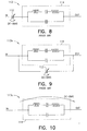
- Figure 8 illustrates an equivalent circuit of a prior art embodiment of a tunable resonator which is connected in series with a tunable capacitor.
- Figure 9 illustrates an equivalent circuit of a prior art embodiment of a tunable resonator which is connected in parallel with a tunable capacitor.
- Figure 10 illustrates an equivalent circuit of a tunable resonator.
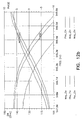
- Figure 11 illustrates phase and amplitude curves of a one port BAW resonator in response to an application of bias voltages of -28 volts, 0 volts, and +28 volts.
- Figure 12a illustrates a portion of the curves of Figure 11, showing in particular the portion of the curves where the series resonance of the BAW resonator occurs.
- Figure 12b illustrates shows a portion of the curves of Figure 11, showing a portion of the curves where the parallel resonance of the resonator occurs.
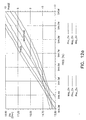
- Figure 13a shows a frequency response of a two port BAW resonator which is connected in parallel.
- Figure 13b illustrates a frequency response of a two port BAW resonator which is connected in parallel.
- Figure 13c illustrates a frequency response of a two port series-connected BAW resonator.
- Figure 13d illustrates a frequency response of a two port series-connected BAW resonator.
- Figure 14a illustrates a frequency response of a series-connected resonator in response to applied DC-bias voltages of +28V, OV, and -28V.
- Figure 14b illustrates a measured spectrum of the resonator of Figure 14a in response to an RF carrier signal having a frequency of 951 MHz and a low frequency modulating signal having a frequency of 600KHz and an amplitude of 8 Vpp.
- Figure 15a illustrates a cross section A-A of a BAW resonator as it appears after a first step of a fabrication process performed in accordance with the invention.
- Figure 15b illustrates a cross-section A-A of the BAW resonator of Figure 15a as it appears after a further step of the fabrication process of Figure 15a.
- Figure 15c illustrates a top view of the BAW resonator of Figure 15b.
- Figure 15d illustrates a cross-section B-B of the BAW resonator of Figure 15b.
- Figure 16a illustrates a cross-section A-A of the BAW resonator of Figure 15a as it appears after a further step of the fabrication process of the invention.
- Figure 16b illustrates a top view of the BAW resonator of Figure 16a.
- Figure 16c illustrates a cross-section B-B of the BAW resonator of Figure 16a.
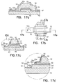
- Figure 17a illustrates a cross-section A-A of the BAW resonator of Figure 16a as it appears after a further step of the fabrication process of the invention.
- Figure 17b illustrates a top view of the BAW resonator of Figure 17a.
- Figure 17c illustrates a cross section B-B of the BAW resonator of Figure 17a.
- Figure 17d illustrates a detail of a portion of the BAW resonator of Figure 17c.
- Fig 18a illustrates a cross section A-A of the BAW resonator of Figure 17a as it appears after a further step of the fabrication process of the invention.
- Figure 18b illustrates top view of the BAW resonator of Figure 18a.
- Figure 18c illustrates a cross-section B-B of the BAW resonator of Figure 18a.
- Figure 19a illustrates a cross-section A-A of the BAW resonator of Figure 18a as it appears after a further step of the fabrication process of the invention.
- Figure 19b illustrates a top view of the BAW resonator of Figure 19a.
- Figure 19c illustrates a cross-section B-B of the BAW resonator of Figure 19a.
- Figure 20 illustrates a cross-section of a BAW resonator that is constructed in accordance with an embodiment of the invention incorporating a sacrificial layer.
- Figure 21 illustrates a BAW resonator that is constructed in accordance with an embodiment of the invention incorporating an acoustic mirror.
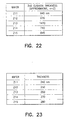
- Figure 22 illustrates a table showing various thicknesses of a layer formed over various types of wafers in accordance with the fabrication process of the invention.
- Figure 23 illustrates a table showing various thicknesses of a tuning layer which may be formed in accordance with the fabrication process of the invention, wherein the thicknesses are shown to correspond to various types of wafers.
- FIGS 2a and 2b illustrate a cross-section A-A (side view) and a top view, respectively, of a Thin Film Bulk Acoustic Wave Resonator (hereinafter referred to as a "BAW resonator” or as an "FBAR") 20 that is constructed in accordance with one embodiment of the invention.
- the BAW resonator 20 comprises a piezoelectric layer 22, a first protective layer 38b, a second protective layer 38a, a first electrode 24, a second electrode 26, a membrane 28, etch windows 40a and 40b, an air gap 34, and a substrate 36.
- a portion of the piezoelectric layer 22 is situated atop the first electrode 24, and the second electrode 26 is situated atop a portion of the piezoelectric layer 22.
- the electrodes 24 and 26 form a parallel plate structure between which the piezoelectric layer 22 is allowed to resonate or vibrate.
- the piezoelectric layer 22 may be comprised of any piezoelectric material that can be fabricated as a thin film such as, by example, zinc-oxide (ZnO), or aluminum-nitride (AIN). In a preferred embodiment of the invention, the piezoelectric layer 22 has a thickness of approximately 1.7 ⁇ m.
- the first and second electrodes 24 and 26 may be comprised of any type of conductive material such as, by example, gold (Au). Each of the first and second electrodes 24 and 26 is preferably 0.1 ⁇ m thick.
- the membrane 28 may comprise one or more layers.
- the membrane 28 comprises two layers, a top layer 30 which is approximately 0.6 ⁇ m thick, and a bottom layer 32 which is approximately 0.4 ⁇ m thick.
- the top layer 30, which has a top surface in contact with the first electrode 24 and with portions of the piezoelectric layer 22, as is illustrated in Figure 2a, is situated atop the bottom layer 32.
- the top layer 30 is preferably comprised of poly-silicon (poly-si) or aluminum-nitride (AIN), and the bottom layer 32 is preferably comprised of silicon-dioxide (SiO 2 ) or gallium arsenide (GaAs).
- these layers may be comprised of any other suitable materials.
- a portion of a bottom surface of the membrane 28 is situated adjacent to the air gap 34, which is formed within a portion of the substrate 36.
- the air gap 34 separates the bottom surface portion of the membrane 28 from a portion of the substrate 36.
- the air gap 34 is bounded by the etch windows 40a and 40b (to be described below), by a portion of the first protective layer 38b (to be described below), by a bottom surface of the membrane 28, and by inner faces 36b, 36c, and 36d of the substrate 36.
- the air gap 34 functions to acoustically isolate vibrations produced by the piezoelectric layer 22 from the substrate 36.
- the substrate 36 may be comprised of any suitable materials such as, by example, silicon (Si), SiO 2 , GaAs, or glass.
- the first protective layer 38b covers a top face 36a of the substrate 36 and portions of the air gap 34.
- a second protective layer 38a covers: (1) the first protective layer 38b, (2) portions of the membrane 28, (3) portions of the piezoelectric layer 22, and (4) portions of the top electrode 26, as can be appreciated in view of Figures 2a and 2b.
- the etch windows 40a and 40b and portions of the first and second electrodes 24 and 26 are exposed to air.
- the first protective layer 38b is comprised of SiO 2 and has a thickness of 0.4 ⁇ m
- the second protective layer 38a is comprised of SiO 2 and has a thickness of 0.2 ⁇ m.
- the etch windows 40a and 40b are formed within the first and second protective layers 38a and 38b on opposite sides of the membrane 28 from one another.
- the etch windows 40a and 40b are created during the fabrication of the resonator 20.
- a portion of the substrate 36 is etched to form the air gap 34 after the membrane layers have been deposited over the substrate 22.
- the air gap 62 may be created by using a sacrificial layer 39 instead of by etching the substrate 36.
- a BAW resonator 21 similar to the one illustrated in Figure 2a is shown, with an addition of the sacrificial layer 39.
- the sacrificial layer 39 is deposited over the substrate 36 prior to the deposition of the membrane 28.
- the sacrificial layer 39 is removed through the etch windows 40a and 40b to form the air gap 34. In this manner, no etching of the substrate needs to be done to create the air gap 34.
- substrates may be employed which comprise various types of materials including, by example, SiO 2 , GaAs, glass, and ceramic materials.
- the piezoelectric layer 22 For each of the resonators 20, and 21, when a voltage is applied across the first and second electrodes 24 and 26, an electric field is created between these electrodes 24 and 26 causing the piezoelectric layer 22 to vibrate.
- the acoustic vibrations produced by the piezoelectric layer 22 propagate from the vibrating piezoelectric layer 22 through the membrane layers 30 and 32. Vibrations reaching the interface between the membrane 28 and the air gap 34 are reflected by this interface back into the membrane 28. In this manner, the air gap 34 isolates vibrations produced by the piezoelectric layer 22 from the substrate.
- a BAW resonator 23 is shown in another embodiment of the invention.
- This resonator 23 has a similar structure as that of the previous embodiment, except that only a single protective layer 38a is provided, and the membrane 28 and the air gap 34 are replaced with an acoustic mirror 70 which acoustically isolates vibrations produced by the piezoelectric layer 22 from the substrate 36.
- This resonator 23 is also referred to a "Solidly Mounted Resonator ("SMR").
- the protective layer 38a comprises, by example, Si0 2 of a thickness of 0.2 ⁇ m.
- the acoustic mirror 70 may comprise one or more layers. In a preferred embodiment of the invention, the acoustic mirror 70 comprises three layers, namely a top layer 70a, a middle layer 70b, and a bottom layer 70c, although additional layers may be employed. Each layer 70a, 70b and 70c has a thickness that is, by example, approximately equal to one quarter wavelength. In a preferred embodiment of the invention, the top layer 70a and bottom layer 70c are comprised of materials having low acoustic impedances such as, by example, silicon (Si), poly-silicon, aluminum (Al), or a polymer.
- the middle layer 70b is comprised of a material having a high acoustic impedance such as, by example, Gold (Au), Molybdenum (Mo), or tungsten (W).
- the acoustic impedance of the middle layer 70b is greater than the acoustic impedance of the top layer 70a.
- the acoustic impedance of the middle layer 70b is greater than the acoustic impedance of the bottom layer 70c.
- the substrate 34 may be comprised of a material having a low impedance such as, by example, Si, Si0 2 , GaAs, glass or a ceramic material.
- the BAW resonator 20 is structurally rugged, permitting high production yields and easier packaging.
- the resonator has a small size, thereby permitting compact resonator layouts on wafers.
- a resonator 80 is provided. A cross-section of this resonator 80 is shown in Figure 3.
- the resonator 80 comprises a piezoelectric layer 82, which is situated between a portion of a top electrode 84 and a portion of a bottom electrode 86.
- the resonator 80 also comprises a membrane 88, and a substrate 90 having a via 92.
- the membrane 88 has a top surface that is positioned adjacent to: (1) a bottom surface of the bottom electrode 86, (2) a portion of a bottom surface of the piezoelectric layer 82, and (3) a portion of a bottom surface of the top electrode 84.
- a bottom surface of the membrane 88 is positioned adjacent to a top surface of the substrate 90 and to a portion of the via 92 formed within the substrate 90.
- An equivalent circuit of the resonator 80 is illustrated in Figure 4
- the resonator 80 functions in a similar manner to the resonator 20 described above in that both of these devices employ air interfaces (i.e., air gap 34 of resonator 20 and via 92 of resonator 80) to reflect acoustic vibrations produced by the respective piezoelectric layers 22 and 82.
- air interfaces i.e., air gap 34 of resonator 20 and via 92 of resonator 80
- a primary difference between these resonators 20 and 80 is the method employed for fabricating the respective air interfaces. For example, during the fabrication process of resonator 80, after materials are deposited forming each of the top electrode 84, the bottom electrode 86, the piezoelectric layer 82, and the membrane 88, a portion of the substrate is then etched away from underneath the substrate 90 to form via 92.
- the membrane 88 may be comprised of, by example, poly-Si or SiO 2 .
- the piezoelectric layer 82, the electrodes 84 and 86, and the substrate 90 may be comprised of materials that are similar to those of the same respective components of resonator 20.
- the size of the via 92 depends upon the area of the resonator 80 and the thickness of the substrate 90. By example, for a case in which the resonator 80 has an area of 200 ⁇ m X 200 ⁇ m, and wherein substrate 90 is comprised of Si with a thickness of 500 ⁇ m, the via 92 area is approximately 900 ⁇ m X 900 ⁇ m.
- a resonator which has the same elements as resonator 80.
- no membrane is provided and, as such, the bottom surface of the bottom electrode, the portion of the bottom surface of the piezoelectric layer, and the portion of the bottom surface of the top electrode are situated directly atop the top surface of the substrate and the portion of the via.
- FIG. 5 illustrates a further embodiment of the invention wherein a resonator 80' is provided which comprises a top electrode 84', a piezoelectric layer 82', a bottom electrode 86', and a substrate 90' comprising a via 92' and a membrane 88'.
- a resonator 80' which comprises a top electrode 84', a piezoelectric layer 82', a bottom electrode 86', and a substrate 90' comprising a via 92' and a membrane 88'.
- These elements are positioned relative to one another in a manner that is similar to the same respective elements of resonator 80, except that membrane 88' is formed by a portion of the substrate located undemeath a portion of the piezoelectric layer 82' and a portion of the bottom electrode 86'.
- the membrane 88' is formed by removing a portion of the substrate by, for example, etching substrate material from underneath the substrate 90' in a similar manner to that described above
- a portion of the substrate 90' which is located adjacent to the portion of the piezoelectric layer 82' and to the portion of the bottom electrode 86' is left un-etched during the fabrication process to form the membrane 88'.
- the resonator 80' functions in a similar manner to the resonator 80 of Figure 3.
- each of the resonators of the previously described embodiments exhibits two distinct resonant frequencies, namely a series resonant frequency and a parallel resonant frequency.
- resonant frequencies are determined by the thicknesses of the individual layers forming the resonators, as well as by the acoustic impedances of the materials forming these layers. For example, thinner resonators exhibit higher resonant frequencies than those exhibited by thicker resonators.
- resonators having layers comprising materials with low acoustic impedances resonate at higher frequencies than resonators comprised of layers having higher acoustic impedances.
- a resonator having a construction similar to the one shown in Figure 2a, but having a piezoelectric material 22 comprised of ZnO with a thickness of 2 ⁇ m, and a layer 32 comprised of Si that is 0.4 ⁇ m thick resonates at a higher frequency than a resonator comprised of similar materials but having a layer 32 that is comprised of SiO 2 having a thickness of 0.4 ⁇ m. This is due to the fact that Si has a lower acoustic impedance than SiO 2 , and thus longitudinal mode acoustic waves travel with greater velocities in Si than in SiO 2 .
- resonators having thinner piezoelectric materials and thicker membranes relative to other resonators have smaller effective coupling coefficients than the other resonators, and have series and parallel resonant frequencies that are closer to one another on the frequency spectrum than those of the other resonators.
- the filter can exhibit a narrow bandwidth.
- Each of the BAW resonators of the invention also has a characteristic acoustic impedance which corresponds to the area of the resonator.
- resonators having large areas have lower characteristic impedances than those having smaller areas.
- the initial steps of the process can be understood in view of Figures 15a-15d, wherein various cross-sections of a substrate 42 and a ZnO layer 44 are shown.
- the substrate 42 is comprised of glass and has a thickness of 100mm.
- ZnO is sputtered over the substrate 42.
- the ZnO is then patterned by wet etching to form a "cushion" having a thickness that is, by example, from 800nm to 1000nm, depending on the type of wafers used, as is shown in the table of Figure 22.
- the ZnO is etched to form gently sloped cushion edges which form sides of the ZnO (cushion edges 44a and 44b are shown). In this manner, a first ZnO layer 44 is formed.
- SiO 2 e.g., PECVD SiO 2
- F plasma fluorine plasma
- the protective photoresist is removed in oxygen plasma.
- the patterning step forms a "tuning layer” 46 or a "first SiO 2 layer".
- the tuning layer 46 is shown in Figure 15b, and may have the various exemplary thicknesses shown in Figure 23 depending on the type of wafer used.
- SiO 2 e.g., PECVD SiO 2
- SiO 2 layer 48 is deposited over the tuning layer 46 and selected portions of the substrate to form a second SiO 2 layer 48 having a thickness of, by example, 400nm.
- SiO 2 layer 48 is collectively referred to as the "SiO 2 layer 48"' in the remaining portion of this description of the fabrication process.
- these layers are collectively labelled by the numeral "48"' in Figures 15c to 19c.
- a next step of the process includes sputtering a metallic element such as, by example, Molybdenum (Mo), over the SiO 2 layer 48'.
- Mo Molybdenum
- the Mo is then patterned by etching in F plasma using a mask layer #3 to form a first layer portion of a bottom electrode (hereinafter referred to as a "first bottom electrode portion") 50.
- the patterning step is performed so that a side 50b of the first bottom electrode portion 50 is horizontally separated from a corner edge 48a of a top surface of layer 48' by a distance of about 20mm.
- Figure 17d illustrates various dimensions of a cross-section B-B of the resonator structure.
- the SiO 2 layer 48' located outside of the perimeter of the first bottom electrode portion 50 may also be etched as needed.
- the first bottom electrode portion 50 may also be covered by, for example, a thin gold film (not illustrated).
- a next step includes sputtering ZnO at high temperature over the first bottom electrode portion 50 and over a selected portion of layer 48'.
- the ZnO is then patterned by wet etching to form a second ZnO layer 52 (i.e., a piezoelectric layer) having a thickness of, by example, 2060nm.
- the patterning step is preferably performed in a manner so that a top surface of the second ZnO layer 52 has a width of, by example, 400 ⁇ m. This can be appreciated in view of Figure 16c which illustrates a cross-section B-B of the resonator.
- the patteming step is preferably performed in a manner such that a bottom surface of the second ZnO layer 52 has edges which are spaced apart from other components of the resonator by particular distances.
- an edge 52b of the second ZnO layer 52 is formed to be horizontally separated from comer edge 48a of the SiO 2 layer 48' by a distance of approximately 40mm.
- an edge 52b of the second ZnO layer 52 is formed to be horizontally separated from side 50b of the first bottom electrode portion layer 50 by a distance of about 20 ⁇ m.
- side 50b of the first bottom electrode portion layer 50 is horizontally separated from a corner edge 48b of the SiO 2 layer 48' by a distance of about 25 ⁇ m.
- a next step of the process includes depositing SiO 2 (e.g., PECVD SiO 2 ) over selected portions of the second ZnO layer 52, over selected portions of the SiO 2 layer 48', and over selected portions of the first bottom electrode portion 50.
- SiO 2 e.g., PECVD SiO 2
- AIN is deposited over the newly deposited SiO 2 layer for an etch stop layer.
- the newly deposited AIN and SiO 2 are then patterned by a wet etching in F plasma to provide an AIN layer 56 (see dark shaded line) and third SiO 2 layer 54 respectively, as are shown in Figures 17a-17d.
- the third SiO 2 layer has a thickness of, by example, 300nm.
- the AIN layer 56 has a thickness of, by example, 50nm. It should be noted that only slight over-etching is performed in order to ensure that the first bottom electrode portion 50 is not damaged.
- the result of the patterning step leaves a portion 52a of a top surface of the second ZnO layer 52 and a portion 50a ( Figure 17a) of a top surface of the first bottom electrode portion 50 exposed to air.
- the patterning step removes portions of the layers 54 and 56, leaving portions of the top surface of the SiO 2 layer 48' exposed to the air.
- the patteming step creates side surfaces 54a and 54b formed by the layers 54 and 56.
- openings A' and B' are formed in the structure on opposite sides of the piezoelectric layer 52, leaving portions of the top surface of layer 48' exposed to air.
- a top electrode 58 and a second layer portion of the bottom electrode are formed by: (a) sputtering molybdenum (Mo) over selected portions of the second ZnO layer 52, over selected portions of the AIN layer 56, and over selected portions of the first bottom electrode portion 50, and (b) patterning the sputtered Mo by etching in F plasma, using a mask level #6 (not illustrated).
- the top electrode 58 and the second bottom electrode portion have thicknesses of, by example, 300nm.
- a next step includes spinning on a protective photoresist and patterning it by etching with a mask #7 (not illustrated) to form vias 41 and 43 ( Figure 19b).
- Dicing grooves are then formed by sawing between chips or wafers as needed, and thereafter the photoresist is removed in, by example acetone.
- the first (cushion) ZnO layer 46 is removed by etching through openings A' and B' in dilute HAc + H 3 PO 4 to form air gap 62.
- the performance characteristics of the resonator may then be tested with testing devices.
- some of the Molybdenum may be removed as needed from the top electrode 58 and the second bottom electrode portion 60 by etching in F plasma. Once these steps have been completed, the wafer may be chipped by breaking along the grooves.
- Resonators included in circuits comprising voltage dependent elements such as, by example, capacitors, are known to exhibit either parallel or series resonant frequencies which vary in frequency when the voltage dependent elements are DC-biased. Examples of two such circuits are illustrated in Figures 6 and 8.
- Figure 6 shows a circuit 110 including a capacitor 112 which is connected in series with a resonator 114 and an active device 116.
- a circuit 113 includes a capacitor 112 connected in series with an equivalent circuit of a resonator 114.
- the resonator 114 acts like a capacitor. At frequencies that are above the series resonant frequency of the resonator 114, the resonator behaves like an inductor. Accordingly, it may be appreciated that the series resonant frequencies of the circuits 110 and 113 can be shifted to above, and not below, the characteristic resonant frequency of the resonator 114. These frequencies are limited to the parallel resonant frequency of the resonator 114.
- FIG. 9 An example of a circuit comprising a resonator connected in parallel with a capacitor is shown in Figure 9.
- a circuit 113a is shown which inciudes an equivalent circuit of a resonator 114 connected in parallel with a capacitor 112.
- the resonator 114 of this circuit 113a exhibits a shift of its parallel resonant frequency in response to a DC-biasing of the capacitor 112 and a resultant voltage being applied across the resonator 114.
- the shift causes the resonator 114 to have a different parallel resonant frequency than the resonator 114 yields without the applied voltage.
- the parallel resonant frequencies of circuit 11 3a can only be tuned to frequencies that are lower than the characteristic parallel resonant frequency of the resonator 114.
- the lower limit of such frequencies is the series resonant frequency of the resonator 114.
- BAW resonators having series and parallel resonant frequencies which shift in response to an applied voltage are referred to as "tunable resonators”.
- BAW resonators in accordance with this invention exhibit shifts in their parallel and series resonant frequencies, and in their impedances in response to DC-bias voltages being applied across the resonators. This occurs in the following manner.
- a bias voltage is applied to the electrodes of one of the resonators, an electric field having a magnitude that is a function of the bias voltage is created within the piezoelectric material located between the electrodes. The electric field causes the piezoelectric material to expand or compress depending upon the polarity of the bias voltage.
- the piezoelectric material exhibits a particular mechanical resonant frequency, a particular impedance, and particular parallel and series resonant frequencies which are different than those exhibited by the piezoelectric material without the effect of the applied DC-bias voltage.
- the application of the varying bias voltage to the resonator causes the electric field to vary as a function of the varying voltage.
- the piezoelectric material is caused to resonate at varying frequencies that are a function of time and the varying voltage, and to exhibit varying impedances that are a function of the varying voltage.
- the bias voltage also may have some effect on parameters that are associated with the piezoelectric material. These parameters can also influence the resonant frequencies.
- the BAW resonators of the instant invention exhibit a maximum phase shift response at particular frequencies which vary as a function of the varying bias voltage.
- FIG. 7 illustrates a circuit 110a including a resonator 114 which exhibits shifts in its impedance and parallel and series resonant frequencies, and which also exhibits a maximum phase shift response at a particular frequency in response to an applied bias voltage.
- Figure 10 illustrates a circuit 113c which includes an equivalent circuit of a resonator (e.g., a BAW resonator) 114 which exhibits similar characteristics.
- a resonator e.g., a BAW resonator
- Figure 11 illustrates a diagram showing measured phase and amplitude curves of an exemplary one port BAW resonator in response to applied bias voltages of -28 volts, 0 volts, and +28. The frequencies range from 942MHz to 952MHz.
- Figure 12a illustrates a portion of the curves of Figure 11, showing, in particular, the portion of the curves where the series resonance of the BAW resonator occurs.
- Figure 12b also shows a similar diagram for the portion of the curves where the parallel resonance of the resonator occurs.
- the tunable BAW resonators of the invention may be utilized in various applications.
- one or more of the resonators may be employed as a voltage dependent feedback element for a voltage controlled oscillator, or as a frequency controlling element in integrated oscillators.
- One or more of the BAW resonators may also be utilized to create a filter having a tunable center frequency (e.g., for dual mode applications).
- a bandpass filter may be synthesized with the resonators.
- the resonators utilized in this application permit the filter to have an approximately fixed bandwidth since the parallel and series resonant frequencies of the resonators are separated by a substantially constant bandwidth.
- the filter and voltage controlled oscillator applications in which the resonators may be employed can be small in size.
- the inventor has determined that when a frequency signal (e.g., in the KHz to MHz range) signal is applied to a BAW resonator, the resonator may be utilized to amplitude modulate or phase modulate higher frequency RF carrier signals of interest.
- a frequency signal e.g., in the KHz to MHz range
- the resonator may be utilized to amplitude modulate or phase modulate higher frequency RF carrier signals of interest.
- Figure 1a which illustrates a device, namely a circuit 91 incorporating a BAW resonator 102 for one of amplitude modulating on phase modulating an RF carrier signal.
- the resonator 102 is connected in parallel with two circuit branches.
- a first one of the branches comprises a generator 90 for generating an RF carrier signal, a bandpass filter 92, and a low frequency blocking capacitor 94.
- the second branch comprises a generator 96 for generating a modulating low frequency signal, a low pass filter 98, and an RF-choke 100.
- the resonator 102 may be any known type of resonator, including by example, one of the resonators illustrated in Figures 2a, 3, and 5.
- the circuit 91 operates in the following manner.
- Generator 96 generates a modulating low frequency signal which varies within a predetermined voltage range (e.g., between -30 volts, 0 volts, and +30 volts) over a specified time period.
- a predetermined voltage range e.g., between -30 volts, 0 volts, and +30 volts
- the low frequency signal is produced, it is filtered by lowpass filter 98, and is thereafter applied to the RF-choke 100 which blocks RF signals.
- the RF-choke 100 then provides the low frequency signal to the remaining portion of circuit 91 comprising resonator 102.
- the resonator 102 has a voltage applied across its electrodes 102a and 102b as a result of the signal.
- the voltage creates an electric field within piezoelectric material 102c between the electrodes 102a and 102b of the resonator 102.
- the electric field magnitude varies as a function of the time-varying voltage applied to the resonator 102 in response to the low frequency signal.
- the electric field effects the piezoelectric material 102c in a manner similar to that described above, causing it to vibrate, which causes a frequency shift of the resonator's series and parallel resonant frequencies and a shift of the resonator's impedance.
- the amounts by which the respective series and parallel resonances and the impedance are shifted are a function of the voltage variation of the low frequency signal and of the electric field variation.
- the bandwidth bounded by the parallel and series resonant frequencies remains substantially constant during the frequency shifts.
- the generator 90 generates an RF carrier signal having a frequency that is between the series and parallel resonant frequencies exhibited by the resonator 102 in response to the applied modulating low frequency signal.
- the generated RF carrier signal has a frequency which is within a frequency range in which the resonator exhibits a minimum phase shift in response to the applied modulating low frequency signal.
- a minimum phase shift occurs at approximately 963MHz.
- a minimum phase shift occurs at approximately 978MHz.
- ideal carrier signal frequencies for these cases are approximately 963MHz and 978MHz, respectively.
- the RF carrier signal is generated by generator 90, it is filtered by the bandpass filter 92, and is then applied to low frequency blocking capacitor 94 which blocks any attendant low frequency signals. Thereafter, the RF carrier signal is supplied to the remaining portion of the circuit 91 comprising the resonator 102.
- the shifting of the impedance and of the series and parallel resonant frequencies exhibited by the resonator 102 in response to the modulating low frequency signal cause a portion of the RF carrier signal traversing the circuit 91 between node 95 and output node 96 to pass through resonator 102.
- the amount of this portion of the RF carrier signal depends upon the varying impedances and resonant frequencies exhibited by the resonator 102.
- the strength of the RF carrier signal travelling between node 95 and output node 96 is attenuated by time-varying amounts which are a function of the voltage variation of the low frequency signal (i.e., the signal experiences a time-dependent, varying amount of insertion loss), thus resulting in an amplitude modulation of the carrier signal.
- a resonator having a frequency response such as that of Figure 13b is employed for performing an amplitude modulation of a 963MHz carrier signal via a 600kHz modulating signal having voltages varying between -V, 0V and +V
- the carrier signal experiences a time-varying insertion loss of approximately ⁇ 2dB (see discussion of Figure 13b below).
- Circuit 93 illustrated in Figure 1b shows another embodiment of a circuit for performing amplitude modulation.
- This circuit 93 comprises similar elements to those of circuit 91, except that resonator 102' is series-connected within the circuit 93, and a coil 104 is shown connected to ground.
- the generator 96 Similar to the operation of circuit 91, the generator 96 generates a low frequency modulating signal and generator 90 generates an RF carrier signal having a frequency that is between the series and parallel resonant frequencies of the resonator 102'.
- the low frequency signal is then applied to elements 98 and 100, and the RF carrier signal is applied to elements 92 and 94, which perform in the same manner as described above.
- the low frequency signal is then applied to resonator 102' which, in response thereto, experiences an electric field between electrodes 102a' and 102b' within piezoelectric material 102c'.
- the electric field causes an impedance shift and a shift of the series and parallel resonant frequencies of the resonator 102' as a function of the voltage variation of the low frequency signal, in a similar manner as described above.
- the RF carrier signal traverses circuit 93 from nodes 95 to resonator 102' and is applied to the resonator 102', the signal then experiences a varying, time-dependent attenuation, and becomes an amplitude modulated signal.
- the amplitude modulated signal is then supplied to output node 96.
- the low frequency signal is directed to a low frequency ground via coil 104.
- the circuit 91 of Figure 1a may also be employed to phase modulate a carrier signal of interest.
- the circuit 91 is operated in a manner similar to that described above, except that the generator 90 generates a carrier signal having a frequency that is preferably approximately equal to the parallel resonant frequency of the shunt-connected resonator 102. This is the frequency of which the resonator 102 resonates and yields its maximum phase shift response as a result of the modulating low frequency signal being applied to the resonator 102.
- an application of a signal having this frequency to the resonator 102 results in a phase shift occurring to the signal by an amount which is a function of the modulating low frequency signal voltage variation.
- a phase shift of approximately ⁇ 28 degrees occurs to a carrier signal having a frequency of approximately 977.5MHz.
- Circuit 93 of Figure 1b may also be employed to phase modulate a carrier signal of interest.
- the circuit 93 is operated in a manner similar to that described above except that generator 90 generates a carrier signal having a frequency that is preferably approximately equal to the series resonant frequency of the series-connected resonator 102'. This is the frequency of which the resonator 102' resonates and yields its maximum phase shift response as a result of the effect of the low frequency signal on the resonator 102'.
- an application of the carrier signal to resonator 102' causes a phase shift to occur to the signal by an amount which is a function of the modulating low frequency signal voltage variation.
- the phase shifted carrier signal is then supplied to output node 96, and the low frequency signal is directed to a low frequency ground via coil 104.
- circuit 91 or circuit 93 is best suited for a particular application depends upon the impedances of the elements forming the respective circuits.
- the shunt connected resonator configuration ( Figure 1a) performs most effectively for a high impedance circuit.
- the BAW resonators of this invention can perform amplitude or phase modulation to RF carrier signals having frequencies in the range from approximately 500MHz to at least 3GHZ, and can operate at an RF power level which is at least ⁇ 30dBm. Moreover, the resonators can perform these modulations in response to low frequency modulating signals having voltages of at least ⁇ 30 volts and frequencies within the KHz to MHz range. Also, at least a 5% amplitude modulation of a carrier signal has been observed in an application employing a ⁇ 28 volt, 600KHz modulating low frequency signal. However, at least a 30% amplitude modulation of an RF carrier signal is achievable.
- the invention can also phase shift a carrier signal by at least one degree per volt of the modulating low frequency signal.
- Figures 13a-13d illustrate frequency responses for various exemplary BAW resonators connected either in series or in parallel, and having two ports of specified impedances.
- the three gain response curves represent the amplitude versus frequency responses to negative, zero, and positive bias voltages, respectively.
- the three phase response curves represent the phase versus frequency responses to negative, zero, and positive bias voltages, respectively.
- Ideal carrier signal frequencies for achieving amplitude modulation and phase modulation for the particular resonators are also indicated.
- frequency response curves of an exemplary two port BAW resonator which is shunt-connected are illustrated.
- the ports have high impedances of 1k0hm.
- the resonator has a layer of ZnO that is 2060nm thick, a layer of SiO 2 that is 400nm thick, and lateral dimensions of 330mm x 330mm.
- Figure 13b illustrates a frequency response of a two port BAW resonator which is shunt-connected.
- the ports have high impedances (e.g., 1kOhm).
- the resonator has a layer of ZnO that is 1650mm thick, a layer of SiO 2 that is 1140nm thick, and lateral dimensions of 330mm x 330mm.
- a low frequency (e.g., 600kHz) signal causes a time-varying insertion loss of approximately ⁇ 2dB to be experienced by a 963MHz carrier signal.
- Figure 13c illustrates a frequency response of a two port BAW resonator which is series-connected.
- the ports have low impedances (e.g., 20 Ohm).
- the resonator has an area of 170mm x 170mm, and has a high impedance.
- Figure 13d illustrates a frequency response of an exemplary two port BAW resonator which is series-connected.
- the ports have low impedances (e.g., 50 Ohm).
- the resonator has an area of 232mm x 232mm, corresponding to an impedance of approximately 50 Ohms.
- an application of a low frequency (e.g., 600KHz) signal to the resonator causes a time dependent insertion loss of approximately ⁇ 3dB to be experienced by a carrier signal having a frequency of 978MHz.
- Figure 14a illustrates a frequency response of a series-connected resonator in response to an applied DC-bias voltage of +28V, OV, and -28V.
- Figure 14b illustrates a measured gain response of the resonator in response to an RF carrier signal having a frequency of 951MHz and a low frequency modulating signal having a frequency of 600KHz and an amplitude of 8 Vpp. Sideband spikes occur at 600kHz as shown in Figure 14b.
Abstract
Description
Figure 7 illustrates a voltage controlled oscillator comprising a resonator and an active device.
Figure 23 illustrates a table showing various thicknesses of a tuning layer which may be formed in accordance with the fabrication process of the invention, wherein the thicknesses are shown to correspond to various types of wafers.
Ls represents the equivalent circuit series inductor of
Claims (15)
- A Bulk Acoustic Wave (BAW) resonator, comprising:a substrate;resonating means;a first electrode situated adjacent to a first surface of said resonating means;a second electrode situated adjacent to a second surface of said resonating means;a membrane situated between said second electrode and said substrate; andan etch window; anda gap separating at least a portion of said substrate from at least a portion of said membrane, said gap being formed by removing a portion of said substrate through said etch window;wherein said resonating means resonates in response to an electric field produced between said first and second electrodes as a result of a voltage that is applied therebetween, and wherein said gap inhibits vibrations produced by said resonating means from said substrate.
- A Bulk Acoustic Wave resonator as set forth in Claim 1, wherein said membrane comprises a first layer and a second layer.
- A Bulk Acoustic Wave resonator as set forth in Claim 2, wherein said first layer comprises at least one of poly-silicon (poly-si) and aluminum nitride (AIN), and wherein said second layer comprises at least one of silicon dioxide (SiO2) and gallium arsenide (GaAs).
- A Bulk Acoustic Wave resonator according to any of the preceding claims, wherein said first and second electrodes are comprised of gold (Au).
- A Bulk Acoustic Wave resonator according to any of the preceding claims, wherein said resonating means comprises at least one of zinc-oxide (ZnO) and aluminum nitride (AIN).
- A Bulk Acoustic Wave resonator according to any of the preceding claims, wherein said substrate comprises at least one of silicon (Si), silicon dioxide (SiO2), gallium arsenide (GaAs), glass, and a ceramic material.
- An amplitude modulator circuit, comprising:a variable voltage generator for generating a low frequency signal having a time-varying voltage;a tunable resonator coupled to said variable voltage generator, said tunable resonator exhibiting parallel and series resonances at frequencies which shift as a function of voltage; andmeans for generating an RF carrier signal having a frequency that is between a parallel resonant frequency and a series resonant frequency exhibited by said tunable resonator in response to a signal output by said variable voltage generator;wherein, in response to both of a the low frequency signal being output by said variable voltage generator and an RF signal being output by said RF carrier signal generator, said tunable resonator causes the RF carrier signal to be attenuated by amounts that are a function of the time-varying voltage of the modulating low frequency signal, thereby amplitude modulating the RF carrier signal.
- An amplitude modulator circuit as set forth in Claim 7, wherein said resonator is connected within said circuit in one of a parallel configuration and a series configuration.
- An amplitude modulator circuit according to claim 7 or claim 8, wherein said RF carrier signal generator generates an RF carrier signal having a frequency which is within a range of frequencies over which said tunable resonator yields a minimum phase shift in response to a signal output by said variable voltage generator.
- A phase modulator circuit, comprising:a variable voltage signal generator for generating a low frequency signal having a time-varying voltage;a tunable resonator, said tunable resonator yielding a maximum phase shift at one of a parallel resonant frequency and a series resonator frequency in response to a modulating low frequency signal output by said variable voltage signal generator; andmeans for generating an RF carrier signal having a frequency that is substantially equal to said one of a parallel resonant frequency and a series resonant frequency;wherein, in response to both of a modulating low frequency signal being output by said variable voltage signal generator and an RF carrier signal being output by said RF carrier signal generator, said tunable resonator causes the RF carrier signal to be phase shifted by an amount that is a function of a variation of the modulating low frequency signal voltage, thereby forming a phase-modulated signal.
- A phase modulator circuit as set forth in Claim 10, wherein said RF carrier signal generator generates a signal having a frequency that is substantially equal to said parallel resonant frequency for a case in which said resonator is connected within said tunable circuit in a parallel configuration, and wherein said RF carrier signal generator generates a signal having said series resonant frequency for a case in which said tunable resonator is connected within said circuit in a series configuration.
- A method for amplitude modulating a signal, comprising the steps of:applying a modulating low frequency signal having a time-varying voltage to a tunable resonator, the tunable resonator exhibiting parallel and series resonances at frequencies which shift by amounts that are a function of the time-varying voltage; andapplying an RF carrier signal having a frequency that is between the parallel resonant frequency and the series resonant frequency to the tunable resonator, wherein in response thereto, the tunable resonator causes the RF carrier signal to be attenuated as a function of the time-varying voltage of the modulating low frequency signal, thereby amplitude modulating said RF carrier signal.
- A method as set forth in Claim 12, wherein the RF carrier signal has a frequency which is approximately equal to one of which the resonator yields a minimum phase shift in response to the modulating low frequency signal.
- A method for phase modulating a signal, comprising the steps of:applying a modulating low frequency signal having a time-varying voltage to a tunable resonator, the tunable resonator yielding a maximum phase shift at one of a parallel resonant frequency and a series resonant frequency in response to the modulating low frequency signal, wherein the amount of phase shift yielded is a function of a variation of the voltage of the modulating low frequency signal; andapplying an RF carrier signal having a frequency that is substantially equal to said one of a parallel resonant frequency and a series resonant frequency, wherein in response thereto, the tunable resonator phase shifts the RF carrier signal by the amount of phase shift yielded by the tunable resonator, thereby phase modulating said RF carrier signal.
- A method as set forth in Claim 14, wherein the RF carrier signal has a frequency that is substantially equal to said series resonant frequency for a case in which the tunable resonator is connected in series, and wherein the RF carrier signal has a frequency that is substantially equal to said parallel resonant frequency for a case in which the tunable resonator is connected in parallel.
Applications Claiming Priority (2)
| Application Number | Priority Date | Filing Date | Title |
|---|---|---|---|
| US720696 | 1996-10-02 | ||
| US08/720,696 US5714917A (en) | 1996-10-02 | 1996-10-02 | Device incorporating a tunable thin film bulk acoustic resonator for performing amplitude and phase modulation |
Publications (3)
| Publication Number | Publication Date |
|---|---|
| EP0834989A2 true EP0834989A2 (en) | 1998-04-08 |
| EP0834989A3 EP0834989A3 (en) | 1998-05-06 |
| EP0834989B1 EP0834989B1 (en) | 2003-09-10 |
Family
ID=24894953
Family Applications (1)
| Application Number | Title | Priority Date | Filing Date |
|---|---|---|---|
| EP97307788A Expired - Lifetime EP0834989B1 (en) | 1996-10-02 | 1997-10-01 | A device incorporating a tunable thin film bulk acoustic resonator for performing amplitude and phase modulation |
Country Status (4)
| Country | Link |
|---|---|
| US (1) | US5714917A (en) |
| EP (1) | EP0834989B1 (en) |
| JP (2) | JPH10126160A (en) |
| DE (1) | DE69724724T2 (en) |
Cited By (12)
| Publication number | Priority date | Publication date | Assignee | Title |
|---|---|---|---|---|
| WO2001006646A1 (en) * | 1999-07-19 | 2001-01-25 | Nokia Corporation | Resonator structure and a filter having such a resonator structure |
| US6204737B1 (en) | 1998-06-02 | 2001-03-20 | Nokia Mobile Phones, Ltd | Piezoelectric resonator structures with a bending element performing a voltage controlled switching function |
| US6242843B1 (en) | 1998-06-02 | 2001-06-05 | Nokia Mobile Phones Ltd. | Resonator structures |
| EP1180494A2 (en) * | 2000-08-11 | 2002-02-20 | Agere Systems Guardian Corporation | Thin film resonators fabricated on membranes created by front side releasing |
| US6388544B1 (en) | 1999-11-29 | 2002-05-14 | Nokia Mobile Phones Ltd. | Method for adjusting the center frequency of a balanced filter and a plurality of balanced filters |
| EP1323232B1 (en) * | 2000-09-25 | 2004-07-14 | Siemens Aktiengesellschaft | Element made of acoustic active material |
| US7378781B2 (en) | 2005-09-07 | 2008-05-27 | Nokia Corporation | Acoustic wave resonator with integrated temperature control for oscillator purposes |
| DE102007028292A1 (en) * | 2007-06-20 | 2008-12-24 | Epcos Ag | Component with reduced voltage attachment |
| CN102830161B (en) * | 2003-12-30 | 2016-12-14 | 英特尔公司 | Utilize the biosensor of the resonator with functionalized surface |
| CN110166018A (en) * | 2018-02-13 | 2019-08-23 | 三星电机株式会社 | Bulk acoustic wave resonator |
| CN111082774A (en) * | 2019-10-23 | 2020-04-28 | 诺思(天津)微系统有限责任公司 | Bulk acoustic wave resonator having electrode with void layer, filter, and electronic device |
| US11973484B2 (en) | 2021-12-31 | 2024-04-30 | Hangzhou Xinghe Technology Co., Ltd. | Acoustic resonator with reinforcing structure and manufacturing method therefor |
Families Citing this family (191)
| Publication number | Priority date | Publication date | Assignee | Title |
|---|---|---|---|---|
| WO1998016956A1 (en) * | 1996-10-17 | 1998-04-23 | Nokia Mobile Phones Limited | Method for fabricating fbars on glass substrates |
| US6081171A (en) * | 1998-04-08 | 2000-06-27 | Nokia Mobile Phones Limited | Monolithic filters utilizing thin film bulk acoustic wave devices and minimum passive components for controlling the shape and width of a passband response |
| GB9815992D0 (en) * | 1998-07-23 | 1998-09-23 | Secr Defence | Improvements in and relating to microchemical devices |
| JP2000209063A (en) * | 1998-11-12 | 2000-07-28 | Mitsubishi Electric Corp | Thin film piezoelectric element |
| US6593831B2 (en) * | 1999-01-14 | 2003-07-15 | The Regents Of The University Of Michigan | Method and apparatus for filtering signals in a subsystem including a power amplifier utilizing a bank of vibrating micromechanical apparatus |
| US6339276B1 (en) * | 1999-11-01 | 2002-01-15 | Agere Systems Guardian Corp. | Incremental tuning process for electrical resonators based on mechanical motion |
| US6746577B1 (en) | 1999-12-16 | 2004-06-08 | Agere Systems, Inc. | Method and apparatus for thickness control and reproducibility of dielectric film deposition |
| US6524971B1 (en) | 1999-12-17 | 2003-02-25 | Agere Systems, Inc. | Method of deposition of films |
| DE19962028A1 (en) * | 1999-12-22 | 2001-06-28 | Philips Corp Intellectual Pty | Filter arrangement |
| US6306313B1 (en) | 2000-02-04 | 2001-10-23 | Agere Systems Guardian Corp. | Selective etching of thin films |
| US6323744B1 (en) | 2000-02-04 | 2001-11-27 | Agere Systems Guardian Corp. | Grounding of TFR ladder filters |
| US7296329B1 (en) | 2000-02-04 | 2007-11-20 | Agere Systems Inc. | Method of isolation for acoustic resonator device |
| US6377136B1 (en) | 2000-02-04 | 2002-04-23 | Agere Systems Guardian Corporation | Thin film resonator filter having at least one component with different resonant frequency sets or electrode capacitance |
| US6437667B1 (en) | 2000-02-04 | 2002-08-20 | Agere Systems Guardian Corp. | Method of tuning thin film resonator filters by removing or adding piezoelectric material |
| WO2001059812A2 (en) * | 2000-02-11 | 2001-08-16 | Siemens Aktiengesellschaft | Assembly comprising a multitude of products each provided with a tunable electronic component, and assembly of devices each comprising such a product |
| EP1273099A1 (en) * | 2000-04-06 | 2003-01-08 | Koninklijke Philips Electronics N.V. | Tunable filter arrangement comprising resonators. |
| JP5175016B2 (en) * | 2000-04-06 | 2013-04-03 | トライクイント・セミコンダクター・インコーポレイテッド | Tunable filter configuration |
| US6603241B1 (en) | 2000-05-23 | 2003-08-05 | Agere Systems, Inc. | Acoustic mirror materials for acoustic devices |
| GB0014963D0 (en) | 2000-06-20 | 2000-08-09 | Koninkl Philips Electronics Nv | A bulk acoustic wave device |
| US6377137B1 (en) | 2000-09-11 | 2002-04-23 | Agilent Technologies, Inc. | Acoustic resonator filter with reduced electromagnetic influence due to die substrate thickness |
| US6486751B1 (en) | 2000-09-26 | 2002-11-26 | Agere Systems Inc. | Increased bandwidth thin film resonator having a columnar structure |
| US6674291B1 (en) * | 2000-10-30 | 2004-01-06 | Agere Systems Guardian Corp. | Method and apparatus for determining and/or improving high power reliability in thin film resonator devices, and a thin film resonator device resultant therefrom |
| US6587212B1 (en) | 2000-10-31 | 2003-07-01 | Agere Systems Inc. | Method and apparatus for studying vibrational modes of an electro-acoustic device |
| US6515558B1 (en) | 2000-11-06 | 2003-02-04 | Nokia Mobile Phones Ltd | Thin-film bulk acoustic resonator with enhanced power handling capacity |
| US6743731B1 (en) * | 2000-11-17 | 2004-06-01 | Agere Systems Inc. | Method for making a radio frequency component and component produced thereby |
| US6424237B1 (en) | 2000-12-21 | 2002-07-23 | Agilent Technologies, Inc. | Bulk acoustic resonator perimeter reflection system |
| US6496085B2 (en) * | 2001-01-02 | 2002-12-17 | Nokia Mobile Phones Ltd | Solidly mounted multi-resonator bulk acoustic wave filter with a patterned acoustic mirror |
| US6407649B1 (en) | 2001-01-05 | 2002-06-18 | Nokia Corporation | Monolithic FBAR duplexer and method of making the same |
| US6518860B2 (en) | 2001-01-05 | 2003-02-11 | Nokia Mobile Phones Ltd | BAW filters having different center frequencies on a single substrate and a method for providing same |
| US6509813B2 (en) | 2001-01-16 | 2003-01-21 | Nokia Mobile Phones Ltd. | Bulk acoustic wave resonator with a conductive mirror |
| US6521100B2 (en) | 2001-02-02 | 2003-02-18 | Nokia Mobile Phones Ltd | Method of producing a piezoelectric thin film and bulk acoustic wave resonator fabricated according to the method |
| US7435613B2 (en) * | 2001-02-12 | 2008-10-14 | Agere Systems Inc. | Methods of fabricating a membrane with improved mechanical integrity |
| US6459067B1 (en) | 2001-04-06 | 2002-10-01 | Eni Technology, Inc. | Pulsing intelligent RF modulation controller |
| US6548943B2 (en) * | 2001-04-12 | 2003-04-15 | Nokia Mobile Phones Ltd. | Method of producing thin-film bulk acoustic wave devices |
| US6476536B1 (en) * | 2001-04-27 | 2002-11-05 | Nokia Corporation | Method of tuning BAW resonators |
| TW506128B (en) * | 2001-06-15 | 2002-10-11 | Asia Pacific Microsystems Inc | Manufacturing method of high-quality thin film type bulk acoustic wave device |
| TWI242883B (en) * | 2001-06-28 | 2005-11-01 | Winbond Electronics Corp | Manufacturing process of high-frequency thin-film bulk acoustic wave filter and apparatus thereof |
| TW573375B (en) * | 2001-12-17 | 2004-01-21 | Intel Corp | Film bulk acoustic resonator structure and method of making |
| US7415483B2 (en) * | 2002-06-05 | 2008-08-19 | Sap Ag | Individual data objects in enterprise computing systems |
| US20040021529A1 (en) * | 2002-07-30 | 2004-02-05 | Bradley Paul D. | Resonator with protective layer |
| US6894360B2 (en) * | 2002-07-30 | 2005-05-17 | Agilent Technologies, Inc. | Electrostatic discharge protection of thin-film resonators |
| US6828713B2 (en) * | 2002-07-30 | 2004-12-07 | Agilent Technologies, Inc | Resonator with seed layer |
| US6944922B2 (en) | 2002-08-13 | 2005-09-20 | Trikon Technologies Limited | Method of forming an acoustic resonator |
| US7152289B2 (en) * | 2002-09-25 | 2006-12-26 | Intel Corporation | Method for forming bulk resonators silicon <110> substrate |
| US6741147B2 (en) * | 2002-09-30 | 2004-05-25 | Agere Systems Inc. | Method and apparatus for adjusting the resonant frequency of a thin film resonator |
| FR2852165A1 (en) * | 2003-03-06 | 2004-09-10 | St Microelectronics Sa | PROCESS FOR PRODUCING A TUNABLE PIEZOLECTRIC MICRORESONATOR |
| US7275292B2 (en) * | 2003-03-07 | 2007-10-02 | Avago Technologies Wireless Ip (Singapore) Pte. Ltd. | Method for fabricating an acoustical resonator on a substrate |
| JP2004304490A (en) * | 2003-03-31 | 2004-10-28 | Tdk Corp | Method and device for manufacturing thin-film piezoelectric resonator, thin-film piezoelectric resonator, and electronic component |
| JP3827232B2 (en) * | 2003-05-13 | 2006-09-27 | Tdk株式会社 | Filter device and duplexer using the same |
| US20040227578A1 (en) * | 2003-05-14 | 2004-11-18 | Miikka Hamalainen | Acoustic resonance-based frequency synthesizer using at least one bulk acoustic wave (BAW) or thin film bulk acoustic wave (FBAR) device |
| JP4053958B2 (en) * | 2003-09-19 | 2008-02-27 | 株式会社東芝 | Voltage controlled oscillator |
| US7332985B2 (en) * | 2003-10-30 | 2008-02-19 | Avago Technologies Wireless Ip (Singapore) Pte Ltd. | Cavity-less film bulk acoustic resonator (FBAR) devices |
| DE602004000851T2 (en) | 2003-10-30 | 2007-05-16 | Avago Technologies General Ip (Singapore) Pte. Ltd. | Acoustically coupled thin film transformer with two piezoelectric elements having opposite C-axes orientation |
| US6946928B2 (en) * | 2003-10-30 | 2005-09-20 | Agilent Technologies, Inc. | Thin-film acoustically-coupled transformer |
| US7391285B2 (en) | 2003-10-30 | 2008-06-24 | Avago Technologies Wireless Ip Pte Ltd | Film acoustically-coupled transformer |
| US7019605B2 (en) * | 2003-10-30 | 2006-03-28 | Larson Iii John D | Stacked bulk acoustic resonator band-pass filter with controllable pass bandwidth |
| FR2864727B1 (en) * | 2003-12-29 | 2007-05-11 | St Microelectronics Sa | ELECTRONIC CIRCUIT COMPRISING A RESONATOR INTENDED TO BE INTEGRATED IN A SEMICONDUCTOR PRODUCT |
| JP2008501248A (en) * | 2004-03-31 | 2008-01-17 | 松下電器産業株式会社 | Acoustic mirror type thin film acoustic wave resonator, and filter, duplexer, and communication device including the same |
| JP4280198B2 (en) | 2004-04-30 | 2009-06-17 | 株式会社東芝 | Thin film piezoelectric resonator |
| US7615833B2 (en) | 2004-07-13 | 2009-11-10 | Avago Technologies Wireless Ip (Singapore) Pte. Ltd. | Film bulk acoustic resonator package and method of fabricating same |
| US7388454B2 (en) | 2004-10-01 | 2008-06-17 | Avago Technologies Wireless Ip Pte Ltd | Acoustic resonator performance enhancement using alternating frame structure |
| US8981876B2 (en) * | 2004-11-15 | 2015-03-17 | Avago Technologies General Ip (Singapore) Pte. Ltd. | Piezoelectric resonator structures and electrical filters having frame elements |
| US7202560B2 (en) | 2004-12-15 | 2007-04-10 | Avago Technologies Wireless Ip (Singapore) Pte. Ltd. | Wafer bonding of micro-electro mechanical systems to active circuitry |
| US7791434B2 (en) * | 2004-12-22 | 2010-09-07 | Avago Technologies Wireless Ip (Singapore) Pte. Ltd. | Acoustic resonator performance enhancement using selective metal etch and having a trench in the piezoelectric |
| US7427819B2 (en) * | 2005-03-04 | 2008-09-23 | Avago Wireless Ip Pte Ltd | Film-bulk acoustic wave resonator with motion plate and method |
| FR2883432B1 (en) * | 2005-03-18 | 2008-02-22 | St Microelectronics Sa | INTEGRABLE FREQUENCY TUNABLE FILTERING CIRCUIT COMPRISING A BAW RESONATOR SET |
| US20060220763A1 (en) * | 2005-03-31 | 2006-10-05 | Tomohiro Iwasaki | Acoustic mirror type thin film bulk acoustic resonator, and filter, duplexer and communication apparatus comprising the same |
| US7369013B2 (en) * | 2005-04-06 | 2008-05-06 | Avago Technologies Wireless Ip Pte Ltd | Acoustic resonator performance enhancement using filled recessed region |
| US7436269B2 (en) * | 2005-04-18 | 2008-10-14 | Avago Technologies Wireless Ip (Singapore) Pte. Ltd. | Acoustically coupled resonators and method of making the same |
| DE102005027715B4 (en) * | 2005-06-15 | 2020-01-02 | Snaptrack, Inc. | Electroacoustic resonator, filter, duplexer and method for determining parameters of a resonator |
| FR2888060A1 (en) * | 2005-07-01 | 2007-01-05 | St Microelectronics Sa | PASS-BAND FILTERING CIRCUIT WITH ACOUSTIC RESONATORS |
| US7868522B2 (en) | 2005-09-09 | 2011-01-11 | Avago Technologies Wireless Ip (Singapore) Pte. Ltd. | Adjusted frequency temperature coefficient resonator |
| DE102005044330A1 (en) * | 2005-09-16 | 2007-03-29 | Epcos Ag | Tunable capacitor and circuit with such a capacitor |
| US7391286B2 (en) * | 2005-10-06 | 2008-06-24 | Avago Wireless Ip Pte Ltd | Impedance matching and parasitic capacitor resonance of FBAR resonators and coupled filters |
| US7525398B2 (en) * | 2005-10-18 | 2009-04-28 | Avago Technologies General Ip (Singapore) Pte. Ltd. | Acoustically communicating data signals across an electrical isolation barrier |
| US7425787B2 (en) | 2005-10-18 | 2008-09-16 | Avago Technologies Wireless Ip (Singapore) Pte. Ltd. | Acoustic galvanic isolator incorporating single insulated decoupled stacked bulk acoustic resonator with acoustically-resonant electrical insulator |
| US7423503B2 (en) * | 2005-10-18 | 2008-09-09 | Avago Technologies Wireless Ip (Singapore) Pte. Ltd. | Acoustic galvanic isolator incorporating film acoustically-coupled transformer |
| US7675390B2 (en) * | 2005-10-18 | 2010-03-09 | Avago Technologies Wireless Ip (Singapore) Pte. Ltd. | Acoustic galvanic isolator incorporating single decoupled stacked bulk acoustic resonator |
| US7737807B2 (en) | 2005-10-18 | 2010-06-15 | Avago Technologies Wireless Ip (Singapore) Pte. Ltd. | Acoustic galvanic isolator incorporating series-connected decoupled stacked bulk acoustic resonators |
| US7463499B2 (en) * | 2005-10-31 | 2008-12-09 | Avago Technologies General Ip (Singapore) Pte Ltd. | AC-DC power converter |
| US7561009B2 (en) * | 2005-11-30 | 2009-07-14 | Avago Technologies General Ip (Singapore) Pte. Ltd. | Film bulk acoustic resonator (FBAR) devices with temperature compensation |
| KR101294844B1 (en) * | 2005-12-29 | 2013-08-08 | 엘지디스플레이 주식회사 | Fabricating method for organic electro-luminescence display device and organic electro-luminescence display device using the same |
| US7612636B2 (en) * | 2006-01-30 | 2009-11-03 | Avago Technologies Wireless Ip (Singapore) Pte. Ltd. | Impedance transforming bulk acoustic wave baluns |
| US7675388B2 (en) * | 2006-03-07 | 2010-03-09 | Agile Rf, Inc. | Switchable tunable acoustic resonator using BST material |
| US7746677B2 (en) * | 2006-03-09 | 2010-06-29 | Avago Technologies Wireless Ip (Singapore) Pte. Ltd. | AC-DC converter circuit and power supply |
| US20070210724A1 (en) * | 2006-03-09 | 2007-09-13 | Mark Unkrich | Power adapter and DC-DC converter having acoustic transformer |
| US7479685B2 (en) * | 2006-03-10 | 2009-01-20 | Avago Technologies General Ip (Singapore) Pte. Ltd. | Electronic device on substrate with cavity and mitigated parasitic leakage path |
| US7629865B2 (en) | 2006-05-31 | 2009-12-08 | Avago Technologies Wireless Ip (Singapore) Pte. Ltd. | Piezoelectric resonator structures and electrical filters |
| FR2901708A1 (en) * | 2006-06-02 | 2007-12-07 | Ela Medical Soc Par Actions Si | ACTIVE MEDICAL DEVICE SUCH AS ACTIVE AMPLANT OR PROGRAMMER FOR SUCH AN IMPLANT, COMPRISING RF EMITTING MEANS |
| FR2904492A1 (en) * | 2006-07-28 | 2008-02-01 | St Microelectronics Sa | Filtering circuit for use in field of mobile telecommunication, has circuit generating two control values i.e. control voltages, that causes two band passes such that bandpass filtering is achieved within range of frequencies |
| US7515018B2 (en) * | 2006-08-31 | 2009-04-07 | Martin Handtmann | Acoustic resonator |
| US7508286B2 (en) * | 2006-09-28 | 2009-03-24 | Avago Technologies Wireless Ip (Singapore) Pte. Ltd. | HBAR oscillator and method of manufacture |
| US7851970B2 (en) * | 2006-12-22 | 2010-12-14 | The Charles Stark Draper Laboratory, Inc. | Structures for crystal packaging including flexible membranes |
| US20080202239A1 (en) * | 2007-02-28 | 2008-08-28 | Fazzio R Shane | Piezoelectric acceleration sensor |
| FR2920612B1 (en) * | 2007-09-03 | 2009-12-04 | St Microelectronics Sa | FREQUENCY TUNING CIRCUIT FOR TRELLIS FILTER |
| US7791435B2 (en) * | 2007-09-28 | 2010-09-07 | Avago Technologies Wireless Ip (Singapore) Pte. Ltd. | Single stack coupled resonators having differential output |
| US7732977B2 (en) * | 2008-04-30 | 2010-06-08 | Avago Technologies Wireless Ip (Singapore) | Transceiver circuit for film bulk acoustic resonator (FBAR) transducers |
| US7855618B2 (en) * | 2008-04-30 | 2010-12-21 | Avago Technologies Wireless Ip (Singapore) Pte. Ltd. | Bulk acoustic resonator electrical impedance transformers |
| US8291559B2 (en) * | 2009-02-24 | 2012-10-23 | Epcos Ag | Process for adapting resonance frequency of a BAW resonator |
| US8902023B2 (en) * | 2009-06-24 | 2014-12-02 | Avago Technologies General Ip (Singapore) Pte. Ltd. | Acoustic resonator structure having an electrode with a cantilevered portion |
| US8248185B2 (en) * | 2009-06-24 | 2012-08-21 | Avago Technologies Wireless Ip (Singapore) Pte. Ltd. | Acoustic resonator structure comprising a bridge |
| KR101634339B1 (en) * | 2009-08-04 | 2016-06-28 | 삼성전자주식회사 | Dual-input dual-output flitering device using bulk acoustic wave resonator and resonance device used as the bulk acoustic wave resonator |
| US8484823B2 (en) * | 2009-08-28 | 2013-07-16 | The Charles Stark Draper Laboratory, Inc. | Methods and apparatus for mounting a crystal |
| KR101616941B1 (en) * | 2009-09-07 | 2016-04-29 | 삼성전자주식회사 | Phase shifter using bulk acoustic wave resonator |
| US8193877B2 (en) * | 2009-11-30 | 2012-06-05 | Avago Technologies Wireless Ip (Singapore) Pte. Ltd. | Duplexer with negative phase shifting circuit |
| US8796904B2 (en) | 2011-10-31 | 2014-08-05 | Avago Technologies General Ip (Singapore) Pte. Ltd. | Bulk acoustic resonator comprising piezoelectric layer and inverse piezoelectric layer |
| US9243316B2 (en) | 2010-01-22 | 2016-01-26 | Avago Technologies General Ip (Singapore) Pte. Ltd. | Method of fabricating piezoelectric material with selected c-axis orientation |
| JP5510465B2 (en) * | 2010-02-09 | 2014-06-04 | 株式会社村田製作所 | Piezoelectric device and method for manufacturing piezoelectric device |
| US8962443B2 (en) | 2011-01-31 | 2015-02-24 | Avago Technologies General Ip (Singapore) Pte. Ltd. | Semiconductor device having an airbridge and method of fabricating the same |
| US9083302B2 (en) | 2011-02-28 | 2015-07-14 | Avago Technologies General Ip (Singapore) Pte. Ltd. | Stacked bulk acoustic resonator comprising a bridge and an acoustic reflector along a perimeter of the resonator |
| US9425764B2 (en) | 2012-10-25 | 2016-08-23 | Avago Technologies General Ip (Singapore) Pte. Ltd. | Accoustic resonator having composite electrodes with integrated lateral features |
| US9048812B2 (en) | 2011-02-28 | 2015-06-02 | Avago Technologies General Ip (Singapore) Pte. Ltd. | Bulk acoustic wave resonator comprising bridge formed within piezoelectric layer |
| US9148117B2 (en) | 2011-02-28 | 2015-09-29 | Avago Technologies General Ip (Singapore) Pte. Ltd. | Coupled resonator filter comprising a bridge and frame elements |
| US9136818B2 (en) | 2011-02-28 | 2015-09-15 | Avago Technologies General Ip (Singapore) Pte. Ltd. | Stacked acoustic resonator comprising a bridge |
| US9203374B2 (en) | 2011-02-28 | 2015-12-01 | Avago Technologies General Ip (Singapore) Pte. Ltd. | Film bulk acoustic resonator comprising a bridge |
| US9154112B2 (en) | 2011-02-28 | 2015-10-06 | Avago Technologies General Ip (Singapore) Pte. Ltd. | Coupled resonator filter comprising a bridge |
| US8575820B2 (en) | 2011-03-29 | 2013-11-05 | Avago Technologies General Ip (Singapore) Pte. Ltd. | Stacked bulk acoustic resonator |
| US9444426B2 (en) | 2012-10-25 | 2016-09-13 | Avago Technologies General Ip (Singapore) Pte. Ltd. | Accoustic resonator having integrated lateral feature and temperature compensation feature |
| US8350445B1 (en) | 2011-06-16 | 2013-01-08 | Avago Technologies Wireless Ip (Singapore) Pte. Ltd. | Bulk acoustic resonator comprising non-piezoelectric layer and bridge |
| US8922302B2 (en) | 2011-08-24 | 2014-12-30 | Avago Technologies General Ip (Singapore) Pte. Ltd. | Acoustic resonator formed on a pedestal |
| US8629036B2 (en) * | 2011-11-11 | 2014-01-14 | International Business Machines Corporation | Integrated semiconductor devices with amorphous silicon beam, methods of manufacture and design structure |
| KR101959204B1 (en) * | 2013-01-09 | 2019-07-04 | 삼성전자주식회사 | Radio frequency filter and manufacturing mathod thereof |
| US9910144B2 (en) * | 2013-03-07 | 2018-03-06 | Cpg Technologies, Llc | Excitation and use of guided surface wave modes on lossy media |
| US9912031B2 (en) | 2013-03-07 | 2018-03-06 | Cpg Technologies, Llc | Excitation and use of guided surface wave modes on lossy media |
| WO2014140409A1 (en) * | 2013-03-11 | 2014-09-18 | Nokia Corporation | Apparatus and method for tuning a resonance frequency |
| CN104471864B (en) * | 2013-06-26 | 2016-04-27 | 英特尔Ip公司 | Bulk acoustic wave resonator tuner circuit |
| JP6180211B2 (en) * | 2013-07-12 | 2017-08-16 | 富士フイルム株式会社 | Diaphragm type resonant MEMS device substrate, diaphragm type resonant MEMS device and manufacturing method thereof |
| WO2015084456A2 (en) * | 2013-09-18 | 2015-06-11 | The Regents Of The University Of California | Tunable q resonator |
| US9793874B2 (en) * | 2014-05-28 | 2017-10-17 | Avago Technologies General Ip Singapore (Singapore) Pte. Ltd. | Acoustic resonator with electrical interconnect disposed in underlying dielectric |
| US9941566B2 (en) | 2014-09-10 | 2018-04-10 | Cpg Technologies, Llc | Excitation and use of guided surface wave modes on lossy media |
| US9887557B2 (en) | 2014-09-11 | 2018-02-06 | Cpg Technologies, Llc | Hierarchical power distribution |
| US10027116B2 (en) | 2014-09-11 | 2018-07-17 | Cpg Technologies, Llc | Adaptation of polyphase waveguide probes |
| US10498393B2 (en) | 2014-09-11 | 2019-12-03 | Cpg Technologies, Llc | Guided surface wave powered sensing devices |
| US9882397B2 (en) | 2014-09-11 | 2018-01-30 | Cpg Technologies, Llc | Guided surface wave transmission of multiple frequencies in a lossy media |
| US10084223B2 (en) | 2014-09-11 | 2018-09-25 | Cpg Technologies, Llc | Modulated guided surface waves |
| US10079573B2 (en) | 2014-09-11 | 2018-09-18 | Cpg Technologies, Llc | Embedding data on a power signal |
| US9893402B2 (en) | 2014-09-11 | 2018-02-13 | Cpg Technologies, Llc | Superposition of guided surface waves on lossy media |
| US10074993B2 (en) | 2014-09-11 | 2018-09-11 | Cpg Technologies, Llc | Simultaneous transmission and reception of guided surface waves |
| US10175203B2 (en) | 2014-09-11 | 2019-01-08 | Cpg Technologies, Llc | Subsurface sensing using guided surface wave modes on lossy media |
| US10001553B2 (en) | 2014-09-11 | 2018-06-19 | Cpg Technologies, Llc | Geolocation with guided surface waves |
| US9960470B2 (en) | 2014-09-11 | 2018-05-01 | Cpg Technologies, Llc | Site preparation for guided surface wave transmission in a lossy media |
| US9887587B2 (en) | 2014-09-11 | 2018-02-06 | Cpg Technologies, Llc | Variable frequency receivers for guided surface wave transmissions |
| US10101444B2 (en) | 2014-09-11 | 2018-10-16 | Cpg Technologies, Llc | Remote surface sensing using guided surface wave modes on lossy media |
| US9887556B2 (en) | 2014-09-11 | 2018-02-06 | Cpg Technologies, Llc | Chemically enhanced isolated capacitance |
| US9859707B2 (en) | 2014-09-11 | 2018-01-02 | Cpg Technologies, Llc | Simultaneous multifrequency receive circuits |
| US10033198B2 (en) | 2014-09-11 | 2018-07-24 | Cpg Technologies, Llc | Frequency division multiplexing for wireless power providers |
| US9923385B2 (en) * | 2015-06-02 | 2018-03-20 | Cpg Technologies, Llc | Excitation and use of guided surface waves |
| US10193595B2 (en) | 2015-06-02 | 2019-01-29 | Cpg Technologies, Llc | Excitation and use of guided surface waves |
| CN108350854B (en) | 2015-09-08 | 2019-11-19 | Cpg技术有限责任公司 | The remote transmission of maritime power |
| US9921256B2 (en) | 2015-09-08 | 2018-03-20 | Cpg Technologies, Llc | Field strength monitoring for optimal performance |
| US9997040B2 (en) | 2015-09-08 | 2018-06-12 | Cpg Technologies, Llc | Global emergency and disaster transmission |
| US9887585B2 (en) | 2015-09-08 | 2018-02-06 | Cpg Technologies, Llc | Changing guided surface wave transmissions to follow load conditions |
| US9857402B2 (en) | 2015-09-08 | 2018-01-02 | CPG Technologies, L.L.C. | Measuring and reporting power received from guided surface waves |
| US9882436B2 (en) | 2015-09-09 | 2018-01-30 | Cpg Technologies, Llc | Return coupled wireless power transmission |
| US10063095B2 (en) | 2015-09-09 | 2018-08-28 | CPG Technologies, Inc. | Deterring theft in wireless power systems |
| US9496921B1 (en) | 2015-09-09 | 2016-11-15 | Cpg Technologies | Hybrid guided surface wave communication |
| EP3345276B1 (en) | 2015-09-09 | 2019-10-09 | CPG Technologies, LLC | Load shedding in a guided surface wave power delivery system |
| US10027131B2 (en) | 2015-09-09 | 2018-07-17 | CPG Technologies, Inc. | Classification of transmission |
| US10205326B2 (en) | 2015-09-09 | 2019-02-12 | Cpg Technologies, Llc | Adaptation of energy consumption node for guided surface wave reception |
| EA201890665A1 (en) | 2015-09-09 | 2018-09-28 | Сипиджи Текнолоджиз, Элэлси. | PROBES OF THE DIRECTED SURFACE WAVEGUIDE |
| WO2017044281A1 (en) | 2015-09-09 | 2017-03-16 | Cpg Technologies, Llc | Guided surface waveguide probes |
| EP3347091B1 (en) | 2015-09-09 | 2020-06-17 | CPG Technologies, LLC. | Power internal medical devices with guided surface waves |
| US9887558B2 (en) | 2015-09-09 | 2018-02-06 | Cpg Technologies, Llc | Wired and wireless power distribution coexistence |
| US9885742B2 (en) | 2015-09-09 | 2018-02-06 | Cpg Technologies, Llc | Detecting unauthorized consumption of electrical energy |
| US10103452B2 (en) | 2015-09-10 | 2018-10-16 | Cpg Technologies, Llc | Hybrid phased array transmission |
| US10559893B1 (en) | 2015-09-10 | 2020-02-11 | Cpg Technologies, Llc | Pulse protection circuits to deter theft |
| US10408916B2 (en) | 2015-09-10 | 2019-09-10 | Cpg Technologies, Llc | Geolocation using guided surface waves |
| US10498006B2 (en) | 2015-09-10 | 2019-12-03 | Cpg Technologies, Llc | Guided surface wave transmissions that illuminate defined regions |
| US10193229B2 (en) | 2015-09-10 | 2019-01-29 | Cpg Technologies, Llc | Magnetic coils having cores with high magnetic permeability |
| KR20180052669A (en) | 2015-09-10 | 2018-05-18 | 씨피지 테크놀로지스, 엘엘씨. | Geo-location using guided surface waves |
| US10408915B2 (en) | 2015-09-10 | 2019-09-10 | Cpg Technologies, Llc | Geolocation using guided surface waves |
| EP3342024A1 (en) | 2015-09-10 | 2018-07-04 | CPG Technologies, LLC | Mobile guided surface waveguide probes and receivers |
| KR20180051573A (en) | 2015-09-10 | 2018-05-16 | 씨피지 테크놀로지스, 엘엘씨. | Global time synchronization using surface wave |
| US10324163B2 (en) | 2015-09-10 | 2019-06-18 | Cpg Technologies, Llc | Geolocation using guided surface waves |
| US10312747B2 (en) | 2015-09-10 | 2019-06-04 | Cpg Technologies, Llc | Authentication to enable/disable guided surface wave receive equipment |
| US10396566B2 (en) | 2015-09-10 | 2019-08-27 | Cpg Technologies, Llc | Geolocation using guided surface waves |
| KR20180051604A (en) | 2015-09-11 | 2018-05-16 | 씨피지 테크놀로지스, 엘엘씨. | Enhanced guided surface waveguide probes |
| EP3338341B1 (en) | 2015-09-11 | 2019-05-29 | CPG Technologies, LLC | Global electrical power multiplication |
| JP2017060077A (en) * | 2015-09-18 | 2017-03-23 | セイコーエプソン株式会社 | Oscillator and method of manufacturing the same |
| US10560147B1 (en) | 2017-03-07 | 2020-02-11 | Cpg Technologies, Llc | Guided surface waveguide probe control system |
| US10630111B2 (en) | 2017-03-07 | 2020-04-21 | Cpg Technologies, Llc | Adjustment of guided surface waveguide probe operation |
| US20200190192A1 (en) | 2017-03-07 | 2020-06-18 | Sutro Biopharma, Inc. | Pd-1/tim-3 bi-specific antibodies, compositions thereof, and methods of making and using the same |
| US10559866B2 (en) | 2017-03-07 | 2020-02-11 | Cpg Technologies, Inc | Measuring operational parameters at the guided surface waveguide probe |
| US10559867B2 (en) | 2017-03-07 | 2020-02-11 | Cpg Technologies, Llc | Minimizing atmospheric discharge within a guided surface waveguide probe |
| US10581492B1 (en) | 2017-03-07 | 2020-03-03 | Cpg Technologies, Llc | Heat management around a phase delay coil in a probe |
| KR20200028034A (en) * | 2017-08-03 | 2020-03-13 | 어쿠스티스, 인크. | Oval structure for bulk acoustic wave resonators |
| JP7037333B2 (en) * | 2017-11-13 | 2022-03-16 | 太陽誘電株式会社 | Elastic wave devices and their manufacturing methods, filters and multiplexers |
| DE102018117520B3 (en) * | 2018-07-19 | 2019-12-05 | RF360 Europe GmbH | RF filter device |
| CN110114971A (en) * | 2019-03-28 | 2019-08-09 | 深圳市汇顶科技股份有限公司 | Crystal oscillator and preparation method thereof and equipment |
| KR20220028297A (en) * | 2020-08-28 | 2022-03-08 | 삼성전기주식회사 | Acoustic resonator filter |
| CN114389563B (en) * | 2021-12-31 | 2022-09-16 | 杭州星阖科技有限公司 | Acoustic wave resonator with reinforcing structure and manufacturing method thereof |
Citations (7)
| Publication number | Priority date | Publication date | Assignee | Title |
|---|---|---|---|---|
| US4019181A (en) * | 1974-07-19 | 1977-04-19 | U.S. Philips Corporation | Transponder system |
| US4320365A (en) * | 1980-11-03 | 1982-03-16 | United Technologies Corporation | Fundamental, longitudinal, thickness mode bulk wave resonator |
| US4456850A (en) * | 1982-02-09 | 1984-06-26 | Nippon Electric Co., Ltd. | Piezoelectric composite thin film resonator |
| US4502932A (en) * | 1983-10-13 | 1985-03-05 | The United States Of America As Represented By The United States Department Of Energy | Acoustic resonator and method of making same |
| US4897618A (en) * | 1989-06-05 | 1990-01-30 | The Curran Company | Harmonic frequency selecting circuit |
| US5166646A (en) * | 1992-02-07 | 1992-11-24 | Motorola, Inc. | Integrated tunable resonators for use in oscillators and filters |
| EP0609555A2 (en) * | 1993-02-01 | 1994-08-10 | Motorola, Inc. | Frequency selective component and method |
Family Cites Families (18)
| Publication number | Priority date | Publication date | Assignee | Title |
|---|---|---|---|---|
| NL277613A (en) * | 1961-04-26 | 1900-01-01 | ||
| US3293557A (en) * | 1964-03-19 | 1966-12-20 | Bell Telephone Labor Inc | Elastic wave devices utilizing mixed crystals of potassium tantalatepotassium niobate |
| US3696312A (en) * | 1970-06-30 | 1972-10-03 | Ibm | Cyclotron resonance devices controllable by electric fields |
| US3686579A (en) * | 1971-06-21 | 1972-08-22 | Zenith Radio Corp | Solid-state, acoustic-wave amplifiers |
| FR2151727A5 (en) * | 1971-09-10 | 1973-04-20 | Thomson Csf | |
| US3833867A (en) * | 1973-10-23 | 1974-09-03 | Sperry Rand Corp | Acoustic surface wave convolver with bidirectional amplification |
| JPS52155036A (en) * | 1976-06-18 | 1977-12-23 | Nec Corp | Elastic surface wave filter |
| JPS56100510A (en) * | 1980-01-16 | 1981-08-12 | Clarion Co Ltd | Elastic surface wave device |
| JPS5972804A (en) * | 1982-10-20 | 1984-04-24 | Matsushita Electric Ind Co Ltd | Surface acoustic wave element |
| JPH0214611A (en) * | 1988-07-01 | 1990-01-18 | Koji Toda | Transversal type signal processing element |
| US5233259A (en) * | 1991-02-19 | 1993-08-03 | Westinghouse Electric Corp. | Lateral field FBAR |
| US5153476A (en) * | 1991-03-11 | 1992-10-06 | The United States Of America As Represented By The Secretary Of The Army | Acoustic vibrator with variable sensitivity to external acceleration |
| US5185589A (en) * | 1991-05-17 | 1993-02-09 | Westinghouse Electric Corp. | Microwave film bulk acoustic resonator and manifolded filter bank |
| JP3198340B2 (en) * | 1991-07-24 | 2001-08-13 | 古野電気株式会社 | Amplitude modulation circuit |
| JPH05206778A (en) * | 1992-01-30 | 1993-08-13 | Hitachi Ltd | Composite filter for surface acoustic wave resonator |
| JP2993266B2 (en) * | 1992-03-24 | 1999-12-20 | 日本電気株式会社 | Amplitude modulator |
| US5446306A (en) * | 1993-12-13 | 1995-08-29 | Trw Inc. | Thin film voltage-tuned semiconductor bulk acoustic resonator (SBAR) |
| JPH10107548A (en) * | 1996-09-30 | 1998-04-24 | Daishinku Co | Frequency modulation device and transmitter-receiver |
-
1996
- 1996-10-02 US US08/720,696 patent/US5714917A/en not_active Expired - Lifetime
-
1997
- 1997-10-01 JP JP9269024A patent/JPH10126160A/en active Pending
- 1997-10-01 DE DE69724724T patent/DE69724724T2/en not_active Expired - Lifetime
- 1997-10-01 EP EP97307788A patent/EP0834989B1/en not_active Expired - Lifetime
-
2007
- 2007-02-22 JP JP2007042874A patent/JP4648911B2/en not_active Expired - Fee Related
Patent Citations (7)
| Publication number | Priority date | Publication date | Assignee | Title |
|---|---|---|---|---|
| US4019181A (en) * | 1974-07-19 | 1977-04-19 | U.S. Philips Corporation | Transponder system |
| US4320365A (en) * | 1980-11-03 | 1982-03-16 | United Technologies Corporation | Fundamental, longitudinal, thickness mode bulk wave resonator |
| US4456850A (en) * | 1982-02-09 | 1984-06-26 | Nippon Electric Co., Ltd. | Piezoelectric composite thin film resonator |
| US4502932A (en) * | 1983-10-13 | 1985-03-05 | The United States Of America As Represented By The United States Department Of Energy | Acoustic resonator and method of making same |
| US4897618A (en) * | 1989-06-05 | 1990-01-30 | The Curran Company | Harmonic frequency selecting circuit |
| US5166646A (en) * | 1992-02-07 | 1992-11-24 | Motorola, Inc. | Integrated tunable resonators for use in oscillators and filters |
| EP0609555A2 (en) * | 1993-02-01 | 1994-08-10 | Motorola, Inc. | Frequency selective component and method |
Non-Patent Citations (2)
| Title |
|---|
| BRANSALOV ET AL: "A monolithic piezoelectric amplitude modulator" INTERNATIONAL JOURNAL OF ELECTRONICS., vol. 47, no. 6, December 1979, LONDON GB, pages 545-553, XP002056874 * |
| LOWE J ET AL: "ULTRALINEAR SMALL-ANGLE PHASE MODULATOR" PROCEEDINGS OF THE ANNUAL SYMPOSIUM ON FREQUENCY CONTROL, LOS ANGELES, MAY 29 - 31, 1991, no. SYMP. 45, 29 May 1991, INSTITUTE OF ELECTRICAL AND ELECTRONICS ENGINEERS, pages 645-648, XP000379325 * |
Cited By (18)
| Publication number | Priority date | Publication date | Assignee | Title |
|---|---|---|---|---|
| US6204737B1 (en) | 1998-06-02 | 2001-03-20 | Nokia Mobile Phones, Ltd | Piezoelectric resonator structures with a bending element performing a voltage controlled switching function |
| US6242843B1 (en) | 1998-06-02 | 2001-06-05 | Nokia Mobile Phones Ltd. | Resonator structures |
| US6788170B1 (en) | 1999-07-19 | 2004-09-07 | Nokia Corporation | Resonator structure having a dampening material and a filter having such a resonator structure |
| WO2001006646A1 (en) * | 1999-07-19 | 2001-01-25 | Nokia Corporation | Resonator structure and a filter having such a resonator structure |
| US6388544B1 (en) | 1999-11-29 | 2002-05-14 | Nokia Mobile Phones Ltd. | Method for adjusting the center frequency of a balanced filter and a plurality of balanced filters |
| EP1180494A2 (en) * | 2000-08-11 | 2002-02-20 | Agere Systems Guardian Corporation | Thin film resonators fabricated on membranes created by front side releasing |
| EP1180494A3 (en) * | 2000-08-11 | 2003-03-26 | Agere Systems Guardian Corporation | Thin film resonators fabricated on membranes created by front side releasing |
| US6847271B2 (en) | 2000-09-25 | 2005-01-25 | Siemens Aktiengesellschaft | Component having an acoustically active material for tuning during operation |
| EP1323232B1 (en) * | 2000-09-25 | 2004-07-14 | Siemens Aktiengesellschaft | Element made of acoustic active material |
| CN102830161B (en) * | 2003-12-30 | 2016-12-14 | 英特尔公司 | Utilize the biosensor of the resonator with functionalized surface |
| US7378781B2 (en) | 2005-09-07 | 2008-05-27 | Nokia Corporation | Acoustic wave resonator with integrated temperature control for oscillator purposes |
| DE102007028292A1 (en) * | 2007-06-20 | 2008-12-24 | Epcos Ag | Component with reduced voltage attachment |
| DE102007028292B4 (en) | 2007-06-20 | 2019-06-19 | Snaptrack, Inc. | Component with reduced voltage attachment |
| CN110166018A (en) * | 2018-02-13 | 2019-08-23 | 三星电机株式会社 | Bulk acoustic wave resonator |
| CN110166018B (en) * | 2018-02-13 | 2023-09-12 | 三星电机株式会社 | Bulk acoustic wave resonator |
| CN111082774A (en) * | 2019-10-23 | 2020-04-28 | 诺思(天津)微系统有限责任公司 | Bulk acoustic wave resonator having electrode with void layer, filter, and electronic device |
| CN111082774B (en) * | 2019-10-23 | 2021-03-12 | 诺思(天津)微系统有限责任公司 | Bulk acoustic wave resonator having electrode with void layer, filter, and electronic device |
| US11973484B2 (en) | 2021-12-31 | 2024-04-30 | Hangzhou Xinghe Technology Co., Ltd. | Acoustic resonator with reinforcing structure and manufacturing method therefor |
Also Published As
| Publication number | Publication date |
|---|---|
| US5714917A (en) | 1998-02-03 |
| JP4648911B2 (en) | 2011-03-09 |
| JPH10126160A (en) | 1998-05-15 |
| JP2007202171A (en) | 2007-08-09 |
| DE69724724T2 (en) | 2004-07-08 |
| DE69724724D1 (en) | 2003-10-16 |
| EP0834989B1 (en) | 2003-09-10 |
| EP0834989A3 (en) | 1998-05-06 |
Similar Documents
| Publication | Publication Date | Title |
|---|---|---|
| EP0834989A2 (en) | A device incorporating a tunable thin film bulk acoustic resonator for performing amplitude and phase modulation | |
| KR100756096B1 (en) | Duplexer | |
| KR100506729B1 (en) | Film bulk acoustic resonator and method for fabrication thereof | |
| US6586861B2 (en) | Film bulk acoustic wave device | |
| EP0616426B1 (en) | Surface acoustic wave device having a lamination structure | |
| US6774746B2 (en) | Thin film bulk acoustic resonator filters with a piezoelectric layer of lead scandium tantalum oxide | |
| US7280007B2 (en) | Thin film bulk acoustic resonator with a mass loaded perimeter | |
| EP1258989A2 (en) | Method of tuning baw resonators | |
| US20040227591A1 (en) | Filter device and method of fabricating a filter device | |
| JP3229336B2 (en) | Acoustic piezoelectric crystals with micromachined surfaces | |
| US7196452B2 (en) | Film acoustic wave device, manufacturing method and circuit device | |
| US7320164B2 (en) | Method of manufacturing an electronic component | |
| US20240088869A1 (en) | Frequency-tunable film bulk acoustic resonator and preparation method therefor | |
| US20070057734A1 (en) | Oscillatory circuit having two oscillators | |
| CA1203860A (en) | Trapped energy resonator for oscillator and multiple resonator applications | |
| JPH11284480A (en) | Piezoelectric thin film resonator | |
| EP1152475A1 (en) | Thin-film piezoelectric device | |
| CN214851161U (en) | Frequency-adjustable film bulk acoustic resonator | |
| Chandrahalim et al. | Fully-differential mechanically-coupled PZT-on-silicon filters | |
| EP0594117B1 (en) | Piezoelectric filter and its production method | |
| KR20000047386A (en) | Method of fabrication acoustic wave device and acoustic wave device using the same | |
| KR100359967B1 (en) | Manufacturing method and circuit device of thin film piezoelectric element and thin film piezoelectric element | |
| Isobe et al. | Radial extensional mode aln-film resonator with high coupling factor | |
| CHATRAS et al. | Large Fractional Bandwidth BAW Filter | |
| JP2002204143A (en) | Ladder type filter and its regulating method |
Legal Events
| Date | Code | Title | Description |
|---|---|---|---|
| PUAI | Public reference made under article 153(3) epc to a published international application that has entered the european phase |
Free format text: ORIGINAL CODE: 0009012 |
|
| PUAL | Search report despatched |
Free format text: ORIGINAL CODE: 0009013 |
|
| AK | Designated contracting states |
Kind code of ref document: A2 Designated state(s): DE FR GB SE |
|
| AK | Designated contracting states |
Kind code of ref document: A3 Designated state(s): AT BE CH DE DK ES FI FR GB GR IE IT LI LU MC NL PT SE |
|
| 17P | Request for examination filed |
Effective date: 19981106 |
|
| AKX | Designation fees paid |
Free format text: DE FR GB SE |
|
| RBV | Designated contracting states (corrected) |
Designated state(s): DE FR GB SE |
|
| 17Q | First examination report despatched |
Effective date: 20001002 |
|
| RAP1 | Party data changed (applicant data changed or rights of an application transferred) |
Owner name: NOKIA CORPORATION |
|
| GRAH | Despatch of communication of intention to grant a patent |
Free format text: ORIGINAL CODE: EPIDOS IGRA |
|
| GRAH | Despatch of communication of intention to grant a patent |
Free format text: ORIGINAL CODE: EPIDOS IGRA |
|
| REG | Reference to a national code |
Ref country code: FR Ref legal event code: ST |
|
| GRAA | (expected) grant |
Free format text: ORIGINAL CODE: 0009210 |
|
| AK | Designated contracting states |
Kind code of ref document: B1 Designated state(s): DE FR GB SE |
|
| REG | Reference to a national code |
Ref country code: GB Ref legal event code: FG4D |
|
| REF | Corresponds to: |
Ref document number: 69724724 Country of ref document: DE Date of ref document: 20031016 Kind code of ref document: P |
|
| REG | Reference to a national code |
Ref country code: SE Ref legal event code: TRGR |
|
| ET | Fr: translation filed | ||
| PLBE | No opposition filed within time limit |
Free format text: ORIGINAL CODE: 0009261 |
|
| STAA | Information on the status of an ep patent application or granted ep patent |
Free format text: STATUS: NO OPPOSITION FILED WITHIN TIME LIMIT |
|
| 26N | No opposition filed |
Effective date: 20040614 |
|
| PGFP | Annual fee paid to national office [announced via postgrant information from national office to epo] |
Ref country code: SE Payment date: 20071004 Year of fee payment: 11 |
|
| PGFP | Annual fee paid to national office [announced via postgrant information from national office to epo] |
Ref country code: FR Payment date: 20071009 Year of fee payment: 11 |
|
| REG | Reference to a national code |
Ref country code: GB Ref legal event code: 732E |
|
| EUG | Se: european patent has lapsed | ||
| REG | Reference to a national code |
Ref country code: FR Ref legal event code: ST Effective date: 20090630 |
|
| PG25 | Lapsed in a contracting state [announced via postgrant information from national office to epo] |
Ref country code: FR Free format text: LAPSE BECAUSE OF NON-PAYMENT OF DUE FEES Effective date: 20081031 |
|
| PG25 | Lapsed in a contracting state [announced via postgrant information from national office to epo] |
Ref country code: SE Free format text: LAPSE BECAUSE OF NON-PAYMENT OF DUE FEES Effective date: 20081002 |
|
| PGFP | Annual fee paid to national office [announced via postgrant information from national office to epo] |
Ref country code: GB Payment date: 20120926 Year of fee payment: 16 |
|
| PGFP | Annual fee paid to national office [announced via postgrant information from national office to epo] |
Ref country code: DE Payment date: 20120927 Year of fee payment: 16 |
|
| REG | Reference to a national code |
Ref country code: DE Ref legal event code: R082 Ref document number: 69724724 Country of ref document: DE Representative=s name: DILG HAEUSLER SCHINDELMANN PATENTANWALTSGESELL, DE |
|
| REG | Reference to a national code |
Ref country code: DE Ref legal event code: R082 Ref document number: 69724724 Country of ref document: DE Representative=s name: DILG HAEUSLER SCHINDELMANN PATENTANWALTSGESELL, DE Effective date: 20130701 Ref country code: DE Ref legal event code: R081 Ref document number: 69724724 Country of ref document: DE Owner name: AVAGO TECHNOLOGIES GENERAL IP (SINGAPORE) PTE., SG Free format text: FORMER OWNER: AVAGO TECHNOLOGIES WIRELESS IP (SINGAPORE) PTE. LTD., SINGAPORE, SG Effective date: 20130701 |
|
| GBPC | Gb: european patent ceased through non-payment of renewal fee |
Effective date: 20131001 |
|
| REG | Reference to a national code |
Ref country code: DE Ref legal event code: R119 Ref document number: 69724724 Country of ref document: DE Effective date: 20140501 |
|
| PG25 | Lapsed in a contracting state [announced via postgrant information from national office to epo] |
Ref country code: GB Free format text: LAPSE BECAUSE OF NON-PAYMENT OF DUE FEES Effective date: 20131001 |
|
| PG25 | Lapsed in a contracting state [announced via postgrant information from national office to epo] |
Ref country code: DE Free format text: LAPSE BECAUSE OF NON-PAYMENT OF DUE FEES Effective date: 20140501 |