KR20200028034A - Oval structure for bulk acoustic wave resonators - Google Patents
Oval structure for bulk acoustic wave resonators Download PDFInfo
- Publication number
- KR20200028034A KR20200028034A KR1020207006244A KR20207006244A KR20200028034A KR 20200028034 A KR20200028034 A KR 20200028034A KR 1020207006244 A KR1020207006244 A KR 1020207006244A KR 20207006244 A KR20207006244 A KR 20207006244A KR 20200028034 A KR20200028034 A KR 20200028034A
- Authority
- KR
- South Korea
- Prior art keywords
- metal plate
- elliptical
- piezoelectric layer
- bottom metal
- resonator
- Prior art date
Links
- 229910052751 metal Inorganic materials 0.000 claims abstract description 58
- 239000002184 metal Substances 0.000 claims abstract description 58
- 238000000034 method Methods 0.000 claims description 26
- 239000000758 substrate Substances 0.000 claims description 19
- 239000000463 material Substances 0.000 claims description 15
- 238000002161 passivation Methods 0.000 claims description 7
- ZOKXTWBITQBERF-UHFFFAOYSA-N Molybdenum Chemical compound [Mo] ZOKXTWBITQBERF-UHFFFAOYSA-N 0.000 claims description 5
- XUIMIQQOPSSXEZ-UHFFFAOYSA-N Silicon Chemical compound [Si] XUIMIQQOPSSXEZ-UHFFFAOYSA-N 0.000 claims description 5
- 229910052750 molybdenum Inorganic materials 0.000 claims description 5
- 239000011733 molybdenum Substances 0.000 claims description 5
- 229910052710 silicon Inorganic materials 0.000 claims description 5
- 239000010703 silicon Substances 0.000 claims description 5
- 229910016570 AlCu Inorganic materials 0.000 claims description 4
- 229910002704 AlGaN Inorganic materials 0.000 claims description 4
- KJTLSVCANCCWHF-UHFFFAOYSA-N Ruthenium Chemical compound [Ru] KJTLSVCANCCWHF-UHFFFAOYSA-N 0.000 claims description 4
- 239000000956 alloy Substances 0.000 claims description 4
- 229910045601 alloy Inorganic materials 0.000 claims description 4
- WPPDFTBPZNZZRP-UHFFFAOYSA-N aluminum copper Chemical compound [Al].[Cu] WPPDFTBPZNZZRP-UHFFFAOYSA-N 0.000 claims description 4
- PMHQVHHXPFUNSP-UHFFFAOYSA-M copper(1+);methylsulfanylmethane;bromide Chemical compound Br[Cu].CSC PMHQVHHXPFUNSP-UHFFFAOYSA-M 0.000 claims description 4
- 229910052707 ruthenium Inorganic materials 0.000 claims description 4
- WFKWXMTUELFFGS-UHFFFAOYSA-N tungsten Chemical compound [W] WFKWXMTUELFFGS-UHFFFAOYSA-N 0.000 claims description 4
- 229910052721 tungsten Inorganic materials 0.000 claims description 4
- 239000010937 tungsten Substances 0.000 claims description 4
- 229910052581 Si3N4 Inorganic materials 0.000 claims description 3
- VYPSYNLAJGMNEJ-UHFFFAOYSA-N Silicium dioxide Chemical compound O=[Si]=O VYPSYNLAJGMNEJ-UHFFFAOYSA-N 0.000 claims description 3
- 239000012212 insulator Substances 0.000 claims description 3
- HBMJWWWQQXIZIP-UHFFFAOYSA-N silicon carbide Chemical compound [Si+]#[C-] HBMJWWWQQXIZIP-UHFFFAOYSA-N 0.000 claims description 3
- HQVNEWCFYHHQES-UHFFFAOYSA-N silicon nitride Chemical compound N12[Si]34N5[Si]62N3[Si]51N64 HQVNEWCFYHHQES-UHFFFAOYSA-N 0.000 claims description 3
- TWNQGVIAIRXVLR-UHFFFAOYSA-N oxo(oxoalumanyloxy)alumane Chemical compound O=[Al]O[Al]=O TWNQGVIAIRXVLR-UHFFFAOYSA-N 0.000 claims description 2
- 229910052594 sapphire Inorganic materials 0.000 claims description 2
- 239000010980 sapphire Substances 0.000 claims description 2
- 229910010271 silicon carbide Inorganic materials 0.000 claims description 2
- 239000003989 dielectric material Substances 0.000 claims 4
- 239000007769 metal material Substances 0.000 claims 4
- 229910052814 silicon oxide Inorganic materials 0.000 claims 1
- 238000003780 insertion Methods 0.000 abstract description 11
- 230000037431 insertion Effects 0.000 abstract description 11
- 230000008878 coupling Effects 0.000 abstract description 7
- 238000010168 coupling process Methods 0.000 abstract description 7
- 238000005859 coupling reaction Methods 0.000 abstract description 7
- 238000010586 diagram Methods 0.000 description 13
- 238000001228 spectrum Methods 0.000 description 8
- 238000012986 modification Methods 0.000 description 7
- 230000004048 modification Effects 0.000 description 7
- 238000011960 computer-aided design Methods 0.000 description 4
- 239000013078 crystal Substances 0.000 description 4
- 229910004298 SiO 2 Inorganic materials 0.000 description 3
- 230000007423 decrease Effects 0.000 description 3
- PIGFYZPCRLYGLF-UHFFFAOYSA-N Aluminum nitride Chemical compound [Al]#N PIGFYZPCRLYGLF-UHFFFAOYSA-N 0.000 description 2
- 239000003990 capacitor Substances 0.000 description 2
- 238000005516 engineering process Methods 0.000 description 2
- 230000000694 effects Effects 0.000 description 1
- 238000004880 explosion Methods 0.000 description 1
- 238000005259 measurement Methods 0.000 description 1
- 239000000203 mixture Substances 0.000 description 1
- 238000010295 mobile communication Methods 0.000 description 1
- 235000012239 silicon dioxide Nutrition 0.000 description 1
- 239000000377 silicon dioxide Substances 0.000 description 1
Images


Classifications
-
- H—ELECTRICITY
- H03—ELECTRONIC CIRCUITRY
- H03H—IMPEDANCE NETWORKS, e.g. RESONANT CIRCUITS; RESONATORS
- H03H9/00—Networks comprising electromechanical or electro-acoustic devices; Electromechanical resonators
- H03H9/02—Details
- H03H9/02007—Details of bulk acoustic wave devices
- H03H9/02086—Means for compensation or elimination of undesirable effects
- H03H9/02149—Means for compensation or elimination of undesirable effects of ageing changes of characteristics, e.g. electro-acousto-migration
-
- H—ELECTRICITY
- H03—ELECTRONIC CIRCUITRY
- H03H—IMPEDANCE NETWORKS, e.g. RESONANT CIRCUITS; RESONATORS
- H03H9/00—Networks comprising electromechanical or electro-acoustic devices; Electromechanical resonators
- H03H9/02—Details
- H03H9/02007—Details of bulk acoustic wave devices
- H03H9/02157—Dimensional parameters, e.g. ratio between two dimension parameters, length, width or thickness
-
- H—ELECTRICITY
- H03—ELECTRONIC CIRCUITRY
- H03H—IMPEDANCE NETWORKS, e.g. RESONANT CIRCUITS; RESONATORS
- H03H9/00—Networks comprising electromechanical or electro-acoustic devices; Electromechanical resonators
- H03H9/02—Details
- H03H9/02007—Details of bulk acoustic wave devices
- H03H9/02086—Means for compensation or elimination of undesirable effects
- H03H9/02118—Means for compensation or elimination of undesirable effects of lateral leakage between adjacent resonators
-
- H—ELECTRICITY
- H03—ELECTRONIC CIRCUITRY
- H03H—IMPEDANCE NETWORKS, e.g. RESONANT CIRCUITS; RESONATORS
- H03H9/00—Networks comprising electromechanical or electro-acoustic devices; Electromechanical resonators
- H03H9/02—Details
- H03H9/05—Holders; Supports
- H03H9/10—Mounting in enclosures
- H03H9/1007—Mounting in enclosures for bulk acoustic wave [BAW] devices
- H03H9/1014—Mounting in enclosures for bulk acoustic wave [BAW] devices the enclosure being defined by a frame built on a substrate and a cap, the frame having no mechanical contact with the BAW device
-
- H—ELECTRICITY
- H03—ELECTRONIC CIRCUITRY
- H03H—IMPEDANCE NETWORKS, e.g. RESONANT CIRCUITS; RESONATORS
- H03H9/00—Networks comprising electromechanical or electro-acoustic devices; Electromechanical resonators
- H03H9/02—Details
- H03H9/125—Driving means, e.g. electrodes, coils
- H03H9/13—Driving means, e.g. electrodes, coils for networks consisting of piezoelectric or electrostrictive materials
- H03H9/131—Driving means, e.g. electrodes, coils for networks consisting of piezoelectric or electrostrictive materials consisting of a multilayered structure
-
- H—ELECTRICITY
- H03—ELECTRONIC CIRCUITRY
- H03H—IMPEDANCE NETWORKS, e.g. RESONANT CIRCUITS; RESONATORS
- H03H9/00—Networks comprising electromechanical or electro-acoustic devices; Electromechanical resonators
- H03H9/02—Details
- H03H9/125—Driving means, e.g. electrodes, coils
- H03H9/13—Driving means, e.g. electrodes, coils for networks consisting of piezoelectric or electrostrictive materials
- H03H9/132—Driving means, e.g. electrodes, coils for networks consisting of piezoelectric or electrostrictive materials characterized by a particular shape
-
- H—ELECTRICITY
- H03—ELECTRONIC CIRCUITRY
- H03H—IMPEDANCE NETWORKS, e.g. RESONANT CIRCUITS; RESONATORS
- H03H9/00—Networks comprising electromechanical or electro-acoustic devices; Electromechanical resonators
- H03H9/15—Constructional features of resonators consisting of piezoelectric or electrostrictive material
- H03H9/17—Constructional features of resonators consisting of piezoelectric or electrostrictive material having a single resonator
- H03H9/171—Constructional features of resonators consisting of piezoelectric or electrostrictive material having a single resonator implemented with thin-film techniques, i.e. of the film bulk acoustic resonator [FBAR] type
- H03H9/172—Means for mounting on a substrate, i.e. means constituting the material interface confining the waves to a volume
-
- H—ELECTRICITY
- H03—ELECTRONIC CIRCUITRY
- H03H—IMPEDANCE NETWORKS, e.g. RESONANT CIRCUITS; RESONATORS
- H03H9/00—Networks comprising electromechanical or electro-acoustic devices; Electromechanical resonators
- H03H9/46—Filters
- H03H9/54—Filters comprising resonators of piezo-electric or electrostrictive material
- H03H9/56—Monolithic crystal filters
- H03H9/564—Monolithic crystal filters implemented with thin-film techniques
-
- H—ELECTRICITY
- H03—ELECTRONIC CIRCUITRY
- H03H—IMPEDANCE NETWORKS, e.g. RESONANT CIRCUITS; RESONATORS
- H03H9/00—Networks comprising electromechanical or electro-acoustic devices; Electromechanical resonators
- H03H9/46—Filters
- H03H9/54—Filters comprising resonators of piezo-electric or electrostrictive material
- H03H9/56—Monolithic crystal filters
- H03H9/566—Electric coupling means therefor
- H03H9/568—Electric coupling means therefor consisting of a ladder configuration
Abstract
타원형 공진기 회로 디바이스. 디바이스는, 하단 금속 플레이트, 하단 금속 층 위에 놓이는 압전 층, 및 압전 층 위에 놓이는 상단 금속 플레이트를 포함한다. 상단 금속 플레이트, 압전 층, 및 하단 금속 플레이트는, 타원 비율(ellipse ratio) R = dx/dy로서 표현될 수 있는, 수평 직경(dx) 및 수직 직경(dy)을 갖는 타원 형상에 의해 특징지어진다. 타원형 구조체를 사용하면, 결과적인 벌크 음향파 공진기(bulk acoustic wave resonator; BAWR)는 통상적인 다각형 공진기들에 비하여 동등하거나 또는 개선된 삽입 손실, 더 높은 결합 계수, 및 더 높은 품질 인자를 나타낼 수 있다.Oval resonator circuit device. The device includes a bottom metal plate, a piezoelectric layer overlying the bottom metal layer, and a top metal plate overlying the piezoelectric layer. The top metal plate, the piezoelectric layer, and the bottom metal plate are characterized by elliptical shapes with horizontal diameter (dx) and vertical diameter (dy), which can be expressed as ellipse ratio R = dx / dy. . Using an elliptical structure, the resulting bulk acoustic wave resonator (BAWR) can exhibit equivalent or improved insertion loss, higher coupling coefficient, and higher quality factor compared to conventional polygonal resonators. .
Description
관련 출원들에 대한 상호 참조들Cross references to related applications
본 출원은, 다음의 가특허 출원: "ELLIPTICAL RESONATOR"라는 명칭으로 2017년 08월 03일자로 출원된 미국 가특허 출원 제62/541,028호에 대한 우선권을 주장하며, 이는 모든 목적들을 위해 참조로서 통합된다.This application claims priority to U.S. Provisional Patent Application No. 62 / 541,028 filed on August 03, 2017 under the provisional provisional patent application: "ELLIPTICAL RESONATOR", which is incorporated by reference for all purposes. do.
기술분야Technology field
본 발명은 전반적으로 전자 디바이스들에 관한 것으로서, 더 구체적으로는 압전 에피택셜(epitaxial) 필름들 및 본질적으로 단결정 필름들에 기초하는 공진기들에 관한 것이다.The present invention relates generally to electronic devices, and more particularly to resonators based on piezoelectric epitaxial films and essentially single crystal films.
모바일 통신 디바이스들이 전 세계적으로 성공적으로 효율적으로 사용되어 왔다. 셀 폰들 및 스마트 폰들을 포함하여 십억 개가 넘는 모바일 디바이스들이 매년 제조되었으며, 유닛 볼륨(unit volume)이 매년 계속해서 증가하고 있다. 약 2012년의 4G/LTE의 램프(ramp) 및 모바일 데이터 트래픽의 폭발과 함께, 데이터 풍부 컨텐츠(data rich content)가 스마트폰 부분의 성장을 이끌고 있으며 - 이는 다음 수년 내에 연간 2B에 도달할 것으로 예상된다. 새로운 표준과 레거시(legacy) 표준의 공존 및 더 높은 데이터 레이트(rate) 요건들에 대한 갈망이 스마트폰들 내의 RF 복잡성을 이끌고 있다. 불행히도, 통상적인 RF 기술을 이용할 때 문제가 되며 장래에 단점들을 초래할 수 있는 한계들이 존재한다.Mobile communication devices have been successfully and efficiently used around the world. More than a billion mobile devices, including cell phones and smart phones, are manufactured each year, and the unit volume continues to increase every year. With the explosion of 4G / LTE ramps and mobile data traffic in about 2012, data rich content is driving the growth of the smartphone segment-expected to reach 2B per year in the next few years do. The coexistence of new and legacy standards and the desire for higher data rate requirements are driving RF complexity in smartphones. Unfortunately, there are limitations that can be problematic when using conventional RF technology and lead to disadvantages in the future.
이상으로부터, 전자 디바이스들을 개선하기 위한 기술들이 강력하게 희망된다는 것이 보여진다.From the above, it has been shown that techniques for improving electronic devices are strongly desired.
본 발명은 전반적으로 전자 디바이스들에 관한 것으로서, 더 구체적으로는 압전 에피택셜 필름들 및 본질적으로 단결정 필름들에 기초하는 공진기들에 관한 것이다.The present invention relates generally to electronic devices, and more particularly to resonators based on piezoelectric epitaxial films and essentially single crystal films.
일 예에 있어서, 본 발명은 타원-형 공진기 디바이스를 제공한다. 디바이스는, 하단 금속 플레이트, 하단 금속 층 위에 놓이는 압전 층, 및 압전 층 위에 놓이는 상단 금속 플레이트를 포함한다. 상단 금속 플레이트, 압전 층, 및 하단 금속 플레이트는, 타원 비율(ellipse ratio) R = dx/dy로서 표현될 수 있는, 수평 직경(dx) 및 수직 직경(dy)을 갖는 타원 형상에 의해 특징지어진다. 특정 예에 있어서, 타원 비율 R은 약 1.20 내지 약 2.00의 범위이다.In one example, the present invention provides an elliptic-type resonator device. The device includes a bottom metal plate, a piezoelectric layer overlying the bottom metal layer, and a top metal plate overlying the piezoelectric layer. The top metal plate, the piezoelectric layer, and the bottom metal plate are characterized by elliptical shapes with horizontal diameter (dx) and vertical diameter (dy), which can be expressed as ellipse ratio R = dx / dy. . In certain examples, the elliptic ratio R ranges from about 1.20 to about 2.00.
복수의 이러한 타원형 공진기 디바이스들은 RF 필터 회로 디바이스 내에 구성될 수 있다. 복수의 마이크로-비아(micro-via)들은 특정 공진기들을 서로 결합하거나 또는 공진기를 상호연결 금속 또는 결합 패드에 결합하도록 구성될 수 있다. 특정 예에 있어서, 본 발명은 11개의 타원형 공진기 디바이스들을 사용하는 RF 필터 구성을 제공하며, 여기에서 7개의 이러한 공진기들은 직렬로 결합되고 4개의 이러한 공진기들은 공진기 직렬 체인의 접합부(junction)들과 접지(ground) 사이에 결합된다. 당업자들은 다른 변형예들, 수정예들, 및 대안예들을 인식할 것이다.A plurality of such elliptical resonator devices can be configured in an RF filter circuit device. The plurality of micro-vias may be configured to couple specific resonators to each other or to couple the resonators to an interconnect metal or bonding pad. In a specific example, the present invention provides an RF filter configuration using eleven elliptical resonator devices, where seven such resonators are coupled in series and four such resonators are grounded with junctions in the resonator series chain. (ground). Those skilled in the art will recognize other variations, modifications, and alternatives.
본 발명을 사용하여 기존의 기술들을 뛰어 넘는 하나 이상의 이점들이 달성된다. 구체적으로, 본 디바이스는 당업계의 일반적인 기술 중 하나에 따라서 통상적인 재료들 및/또는 방법들을 사용하여 상대적으로 간단하고 비용 효율적인 방식으로 제조될 수 있다. 본 방법을 사용하면, 통상적인 다각형 공진기들에 비하여 동등하거나 또는 개선된 삽입 손실을 갖는 개선된 벌크 음향파 공진기(bulk acoustic wave resonator; BAWR)를 생성할 수 있다. 이러한 필터들 또는 공진기들은 RF 필터 디바이스, RF 필터 시스템, 또는 유사한 것 내에 구현될 수 있다. 실시예에 의존하여, 이러한 이점들 중 하나 이상이 달성될 수 있다. 물론, 다른 변형예들, 수정예들, 및 대안예들이 존재할 수 있다.One or more advantages over existing techniques are achieved using the present invention. Specifically, the device can be manufactured in a relatively simple and cost effective manner using conventional materials and / or methods according to one of the general techniques in the art. Using this method, an improved bulk acoustic wave resonator (BAWR) with equivalent or improved insertion loss compared to conventional polygonal resonators can be produced. These filters or resonators may be implemented in an RF filter device, RF filter system, or similar. Depending on the embodiment, one or more of these advantages can be achieved. Of course, other variations, modifications, and alternatives may exist.
본 발명의 성질 및 이점들의 더 큰 이해는 첨부된 도면 및 이후의 상세한 설명의 부분들을 참조함으로써 인식될 수 있다.A greater understanding of the nature and advantages of the present invention can be appreciated by referring to the accompanying drawings and portions of the detailed description that follows.
본 발명을 더 완전하게 이해하기 위하여, 첨부된 도면들에 대한 참조가 이루어진다. 이러한 도면들이 본 발명의 범위에 있어서의 제한들로서 여겨지지 않아야 하며, 본 발명의 현재 설명되는 실시예들 및 현재 이해되는 최적의 모드가 첨부된 도면들을 사용하여 추가적인 세부사항들과 함께 설명된다는 것이 이해되어야 한다.
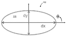
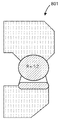
도 1a 및 도 1b는 각기, 본 발명의 일 예에 따른 타원형 공진기에 대한, 측면도 및 상단도를 예시하는 간략도들이다.
도 2는 본 발명의 다양한 예들에 따른 몇몇 타원형 공진기들을 사용하는 RF 필터 회로 디바이스를 예시하는 간략도이다.
도 3a는 본 발명의 일 예에 따른 A-B 기준 라인을 따른 도 2의 RF 필터 회로의 단면도를 예시하는 간략도이다.
도 3b는 본 발명의 일 예에 따른 A-B 기준 라인을 따른 도 2의 RF 필터 회로의 단면도를 예시하는 간략도이다.
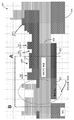
도 4는 본 발명의 일 예에 따른 타원형 공진기들을 사용하는 RF 필터 디바이스의 컴퓨터-지원 설계(computer-aided design; CAD) 레이아웃(layout)이다.
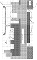
도 5는 본 발명의 일 예에 따른 타원형 공진기들을 사용하는 RF 필터 회로의 물리적 구현예의 이미지이다.
도 6은 본 발명의 일 예에 따른 타원형 공진기 구성형 RF 필터 회로를 예시하는 간략화된 회로도이다.
도 7a는 본 발명의 일 예에 따른 타원형 공진기(R=1.61)에 대한 필터 통과대역 대 통상적인 다각형 공진기에 대한 필터 통과대역의 삽입 손실을 비교하는 그래프이다.
도 7b는 본 발명의 일 예에 따른 타원형 공진기(R=1.61)에 대한 필터 협대역 스펙트럼 대 통상적인 다각형 공진기에 대한 필터 협대역 스펙트럼의 삽입 손실을 비교하는 그래프이다.
도 7c는 본 발명의 일 예에 따른 타원형 공진기(R=1.61)에 대한 필터 광대역 스펙트럼 대 통상적인 다각형 공진기에 대한 필터 광대역 스펙트럼의 삽입 손실을 비교하는 그래프이다.
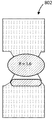
도 8a 내지 도 8d는 다양한 비율의 R을 가지고 구성된 타원형 공진기들을 예시하는 간략도들이다.
도 9a 및 도 9b는 각기, 본 발명의 일 예에 따른 타원형 공진기와 통상적인 다각형 공진기 사이의, 결합 계수(coupling coefficient) 및 품질 인자(quality factor)를 비교하는 그래프들이다.
도 9c는 도 9a 및 도 9b에 도시된 그래프들로부터의 결과들을 요약하는 표이다.In order to more fully understand the present invention, reference is made to the accompanying drawings. It should be understood that these drawings are not to be regarded as limitations in the scope of the present invention, and that the presently described embodiments of the present invention and the best mode currently understood are described with additional details using the accompanying drawings. Should be.
1A and 1B are schematic diagrams respectively illustrating a side view and a top view of an elliptical resonator according to an example of the present invention.
2 is a simplified diagram illustrating an RF filter circuit device using some elliptical resonators in accordance with various examples of the present invention.
3A is a simplified diagram illustrating a cross-sectional view of the RF filter circuit of FIG. 2 along the AB reference line according to an example of the present invention.
3B is a simplified diagram illustrating a cross-sectional view of the RF filter circuit of FIG. 2 along the AB reference line according to an example of the present invention.
4 is a computer-aided design (CAD) layout of an RF filter device using elliptical resonators according to an example of the present invention.
5 is an image of a physical implementation of an RF filter circuit using elliptical resonators according to an example of the present invention.
6 is a simplified circuit diagram illustrating an oval resonator component RF filter circuit according to an example of the present invention.
7A is a graph comparing the insertion loss of a filter passband for a conventional polygonal resonator versus a filter passband for an elliptical resonator (R = 1.61) according to an example of the present invention.
7B is a graph comparing the insertion loss of a filter narrowband spectrum for an elliptical resonator (R = 1.61) versus a filter narrowband spectrum for a conventional polygonal resonator according to an example of the present invention.
7C is a graph comparing the insertion loss of a filter broadband spectrum for an elliptical resonator (R = 1.61) versus a filter broadband spectrum for a conventional polygonal resonator according to an example of the present invention.
8A-8D are simplified diagrams illustrating elliptical resonators constructed with various ratios of R.
9A and 9B are graphs comparing a coupling coefficient and a quality factor between an elliptical resonator and a conventional polygonal resonator according to an example of the present invention, respectively.
9C is a table summarizing the results from the graphs shown in FIGS. 9A and 9B.
본 발명은 전반적으로 전자 디바이스들에 관한 것으로서, 더 구체적으로는 압전 에피택셜 필름들 및 본질적으로 단결정 필름들에 기초하는 공진기들에 관한 것이다.The present invention relates generally to electronic devices, and more particularly to resonators based on piezoelectric epitaxial films and essentially single crystal films.
일반적으로, 벌크 음향파 공진기(Bulk Acoustic Wave Resonator; BAWR)는, 커패시터의 2개의 전극들 사이의 압전 재료의 조성 및 그것의 금속 플레이트들의 기하학적 형상 및 두께에 의해 특징지어질 수 있는 평행 플레이트 커패시터이다. 이러한 공진기들의 구성은, RF 회로 내에 필터를 위치시키는 것의 영향을 설명하는 ("S21"로서 알려진) 삽입 손실에 의해 특징지어지는 신호 통과대역을 생성하는 RF 필터를 생성하기 위해 사용될 수 있다.Generally, a bulk acoustic wave resonator (BAWR) is a parallel plate capacitor that can be characterized by the composition of the piezoelectric material between the two electrodes of the capacitor and the geometry and thickness of its metal plates. . The configuration of these resonators can be used to create an RF filter that produces a signal passband characterized by insertion loss (known as "S21") that accounts for the effect of placing the filter in the RF circuit.
통상적인 공진기들은 전형적으로 N-개의 측면들(여기에서 N≥3)을 갖는 다각형들을 사용하여 구성된다. 원형 공진기들이 가능하지만, 전형적으로, 이는 공진기 내에서 바람직하지 않은 모드들을 초래하는 바람직하지 않은 대칭성을 제공한다. 그러나, 타원형 공진기들은, 공진기의 수평 직경(dx) 대 수직 직경(dy)의 비율(R로서 정의됨)을 가지고 구성될 수 있으며, 여기에서 R = dx/dy이다. 일단 R을 가지고 정의되면, 공진기는 임의적인 각도 세타(θ)로 RF 회로 내에 위치될 수 있다.Conventional resonators are typically constructed using polygons with N-sides (N ≧ 3 here). Circular resonators are possible, but typically, this provides undesirable symmetry resulting in undesirable modes within the resonator. However, the elliptical resonators can be constructed with a ratio (defined as R) of the horizontal diameter (dx) to the vertical diameter (dy) of the resonator, where R = dx / dy. Once defined with R, the resonator can be placed in the RF circuit at an arbitrary angle theta (θ).
본 발명의 예들에 따르면, 약 1.60 내지 약 1.61 사이의 R의 고유 비율을 갖는 타원형 공진기들을 사용하는 단결정 압전-기반 RF 필터들은, 통상적인 다각형 공진기들과 비교할 때 동등하거나 또는 개선된 삽입 손실 성능을 제공하도록 제조되고 테스트되었다. 이러한 필터들은 약 0.4 GHz 내지 약 20 GHz의 범위의 중심 주파수에 의해 특징지어지며, 필터 회로의 전기적 임피던스를 조정하기 위하여 하나 이상의 영역들을 사용한다.According to the examples of the present invention, single crystal piezoelectric-based RF filters using elliptical resonators having an intrinsic ratio of R between about 1.60 and about 1.61 have equivalent or improved insertion loss performance compared to conventional polygonal resonators. It was manufactured and tested to provide. These filters are characterized by a center frequency in the range of about 0.4 GHz to about 20 GHz, and use one or more regions to adjust the electrical impedance of the filter circuit.
도 1a는 본 발명의 일 예에 따른 타원형 공진기의 측면 "샌드위치" 도면을 예시하는 간략도이다. 도시된 바와 같이, 디바이스(101)는 압전 층(130)을 샌드위치하는 상단 금속 플레이트(110) 및 하단 금속 플레이트(120)를 포함한다. 도 1b는 본 발명의 일 예에 따른 동일한 타원형 공진기의 상단도를 예시하는 간략도이다. 여기에서, 디바이스(102)는 단지 상단 금속 플레이트(110)만을 도시하지만, 수평 직경(dx), 수직 직경(dy) 및 각도 세타(θ)의 이상에서 논의된 측정치들이 상단 금속 플레이트(110)와 관련하여 도시된다.1A is a simplified diagram illustrating a side view “sandwich” of an elliptical resonator according to an example of the present invention. As shown, the
도 2는 본 발명의 다양한 예들에 따른 몇몇 타원형 공진기들을 사용하는 RF 필터 회로 디바이스를 예시하는 간략도이다. 도시된 바와 같이, 디바이스(200)는 회로 다이(die)(210) 상에 구성된 몇몇 타원형 공진기들(220)을 포함한다. 특정 예에 있어서, 회로 다이(또는 기판)는, 실리콘 기판, 사파이어 기판, 탄화 실리콘 기판, GaN 벌크 기판, GaN 템플릿(template), AlN 템플릿, AlxGa1-xN 템플릿들, 엔지니어링된(engineered) 기판들 예컨대 실리콘 온 절연체(silicon on insulator; SOI), 및 다결정질 AlN 템플릿들로부터 선택된다. 이러한 공진기들(220)은 비아들(230)에 의해 서로 또는 오프-칩 연결들에 연결될 수 있다. 이러한 예에 있어서, 유전체 패시베이션(passivation) 층(211)이 회로 다이(210) 위에 놓이도록 형성되며, 이는 실리콘 이산화물(SiO2), 실리콘 질화물(SiN), 알루미늄 질화물(AlN), 또는 알루미늄 산화물(AlO), 또는 유사한 것일 수 있다. SiO2의 사용은 RF 필터 회로 내의 온도 드리프트(temperature drift)를 개선할 수 있다. 당업자들은 다른 변형예들, 수정예들, 및 대안예들을 인식할 것이다.2 is a simplified diagram illustrating an RF filter circuit device using some elliptical resonators in accordance with various examples of the present invention. As shown,
도 3a는 본 발명의 일 예에 따른 A-B 기준 라인을 따른 도 2의 RF 필터 회로의 단면도를 예시하는 간략도이다. 도시된 바와 같이, 디바이스(301)는, 실리콘 탄화물(SiC) 재료 또는 유사한 것을 포함할 수 있는 기판(310) 위에 놓이는 타원형 공진기 디바이스(320), 및 SiO2 또는 유사한 것을 포함할 수 있는 유전체 패시베이션 층(311)을 포함한다. 공진기 디바이스(320)는, 알루미늄 질화물(AlN) 재료 또는 유사한 것을 포함할 수 있는, 압전 층(323)을 샌드위치하는 상단 금속 플레이트(상단 전극)(321) 및 하단 금속 플레이트(하단 전극)(322)를 포함한다. 특정 예에 있어서, 압전 층은: AlN, AlGaN, GaN, InN, InGaN, AlInN, AlInGaN, ScAlN, ScGaN, AlScYN, 및 BN 중 적어도 하나를 갖는 재료들 또는 합금들을 포함한다. 마이크로-비아(330)는, 마이크로-비아(330)를 하단 금속 플레이트(322)에 결합하는, 몰리브데넘 재료 또는 유사한 것을 포함할 수 있는, 후면 금속 상호연결부(331)를 가지고 이러한 공진기(320)에 인접하여 구성된다.3A is a simplified diagram illustrating a cross-sectional view of the RF filter circuit of FIG. 2 along the AB reference line according to an example of the present invention. As shown, the
특정 예에 있어서, 공진기(320)는 또한 2가지 유형의 에너지 구속 특징부(energy confinement feature; ECF), 즉, ECF-1(341) 및 ECF-2(342)를 포함한다. ECF-1(341)은 상단 금속 플레이트 표면 상에 하나 이상의 필러(pillar) 구조체들을 포함하며, 반면 ECF-2(342)는 상단 금속 전극 표면 내에 하나 이상의 캐비티(cavity) 영역들을 포함한다. 이러한 ECF 구조체들은 또한 하단 금속 플레이트 상에도 마찬가지로 형성될 수 있다. 특정 예에 있어서, 하단 금속 플레이트, 상단 금속 플레이트, 및 ECF 구조체들은 몰리브데넘(Mo), 루테늄(Ru), 알루미늄 구리(AlCu), 또는 텅스텐(W), 또는 유사한 것을 포함할 수 있다. 물론, 다른 변형예들, 수정예들, 및 대안예들이 존재할 수 있다.In a particular example,
도 3b는 본 발명의 일 예에 따른 A-B 기준 라인을 따른 도 2의 RF 필터 회로의 단면도를 예시하는 간략도이다. 도시된 바와 같이, 디바이스(302)는, 임의의 ECF-2 구조체들 없이 ECF-1 구조체들만이 존재한다는 점을 제외하면 디바이스(301)와 유사하다. 나머지 엘리먼트들은 도 3a의 것들과 동일한 참조 번호 기법을 따른다.3B is a simplified diagram illustrating a cross-sectional view of the RF filter circuit of FIG. 2 along an A-B reference line according to an example of the present invention. As shown,
도 4는 본 발명의 일 예에 따른 타원형 공진기들을 사용하는 RF 필터 디바이스의 컴퓨터-지원 설계(CAD) 레이아웃이다. 이미지(400)는 도 1의 레이아웃과 유사한 레이아웃을 보여준다. 도 5는 본 발명의 일 예에 따른 타원형 공진기들을 사용하는 RF 필터 회로의 물리적 구현예의 이미지이다. 이미지(500)는 비교 목적들을 위하여 도 4와 동일한 배향으로 구성된다.4 is a computer-aided design (CAD) layout of an RF filter device using elliptical resonators according to an example of the present invention.
도 6은 본 발명의 일 예에 따른 타원형 공진기 구성형 RF 필터 회로를 예시하는 간략화된 회로도이다. 도시된 바와 같이, 디바이스(600)는 그 사이에 구성된 타원형 공진기들(620)을 갖는 RF 필터 입력(601) 및 RF 필터 출력(602)을 포함한다. 특정 예에 있어서, RF 필터는 11개의 이러한 공진기들을 포함하며, 여기에서 7개의 공진기들은 입력과 출력 사이에 직렬로 존재하며 4개의 공진기들은 접지 및 직렬 구성들의 상호연결부에 연결된다. 물론, 다른 변형예들, 수정예들, 및 대안예들이 존재할 수 있다.6 is a simplified circuit diagram illustrating an oval resonator component RF filter circuit according to an example of the present invention. As shown, the
도 7a는 본 발명의 일 예에 따른 타원형 공진기(R=1.61)에 대한 필터 통과대역 대 통상적인 다각형 공진기에 대한 필터 통과대역의 삽입 손실을 비교하는 그래프이다. 통상적인 다각형 공진기에 대한 결과들은 플롯(710)에 의해 도시되며, 반면 타원형 공진기에 대한 결과들은 플롯(720)에 의해 도시된다.7A is a graph comparing the insertion loss of a filter passband for a conventional polygonal resonator versus a filter passband for an elliptical resonator (R = 1.61) according to an example of the present invention. Results for a typical polygonal resonator are shown by
도 7b는 본 발명의 일 예에 따른 타원형 공진기(R=1.61)에 대한 필터 협대역 스펙트럼 대 통상적인 다각형 공진기에 대한 필터 협대역 스펙트럼의 삽입 손실을 비교하는 그래프이다. 통상적인 다각형 공진기에 대한 결과들은 플롯(710)에 의해 도시되며, 반면 타원형 공진기에 대한 결과들은 플롯(720)에 의해 도시된다.7B is a graph comparing the insertion loss of a filter narrowband spectrum for an elliptical resonator (R = 1.61) versus a filter narrowband spectrum for a conventional polygonal resonator according to an example of the present invention. Results for a typical polygonal resonator are shown by
도 7c는 본 발명의 일 예에 따른 타원형 공진기(R=1.61)에 대한 필터 광대역 스펙트럼 대 통상적인 다각형 공진기에 대한 필터 광대역 스펙트럼의 삽입 손실을 비교하는 그래프이다. 통상적인 다각형 공진기에 대한 결과들은 플롯(710)에 의해 도시되며, 반면 타원형 공진기에 대한 결과들은 플롯(720)에 의해 도시된다.7C is a graph comparing the insertion loss of a filter broadband spectrum for an elliptical resonator (R = 1.61) versus a filter broadband spectrum for a conventional polygonal resonator according to an example of the present invention. Results for a typical polygonal resonator are shown by
도 8a 내지 도 8d는 다양한 비율의 R을 가지고 구성된 타원형 공진기들을 예시하는 간략도들이다. 도 8a는 R = 1.2의 타원 비율을 갖는 디바이스(801)를 예시한다. 도 8b는 R = 1.6의 타원 비율을 갖는 디바이스(802)를 예시한다. 도 8c 및 도 8d는 각기 R = 1.8 및 R = 2.0의 타원 비율들을 갖는 디바이스들(803 및 804)을 예시한다.8A-8D are simplified diagrams illustrating elliptical resonators constructed with various ratios of R. 8A illustrates
본 발명의 예들은, BAW 공진기의 형상이 전체 성능을 결정한다는 사실을 이용한다. 측방 모드 잡음은 형상의 전체 대칭성이 감소함에 따라 감소되며, 즉, 타원 형상은 원형 형상들보다 더 약한 측방 모드 잡음을 보여준다. 사변형 또는 오각형 형상들의 코너들에서의 음향파의 약한 수직 진폭은 공진기의 결합 계수를 감소시키며, 그에 따라서, 타원형 공진기는 더 높은 결합 계수를 가능하게 하도록 코너들을 제거한다. 추가로, 면적-대-에지(area-to-edge)의 비율은, 음향파가 에지를 따라 공진기의 외부로 방사될 때 공진기의 품질 인자에 영향을 준다. 타원이 사변형 또는 다른 다각형 형상에 비하여 주어진 면적에 대해 더 짧은 에지를 가지기 때문에, 타원형 공진기는 마찬가지로 더 높은 품질 인자를 나타낼 수 있다.Examples of the present invention take advantage of the fact that the shape of the BAW resonator determines the overall performance. The lateral mode noise decreases as the overall symmetry of the shape decreases, that is, the elliptical shape shows weaker lateral mode noise than circular shapes. The weak vertical amplitude of the acoustic wave at the corners of the quadrilateral or pentagonal shapes reduces the coupling coefficient of the resonator, and accordingly, the elliptical resonator removes the corners to enable a higher coupling coefficient. Additionally, the area-to-edge ratio affects the quality factor of the resonator when acoustic waves are emitted along the edge to the outside of the resonator. Because ellipses have shorter edges for a given area compared to quadrilaterals or other polygonal shapes, elliptical resonators can likewise exhibit higher quality factors.
특정 예에 있어서, R = 1.6의 특정 종횡비를 갖는 타원형 공진기는 반공진 주파수(anti-resonance frequency)(Qp) 근처에서 더 양호한 품질 인자를 나타낸다. 5 GHz 근처의 공진 주파수를 갖는 BAW 공진기들로부터의 데이트(date)는, 타원의 종횡비가 1.6일 때 더 높은 Qp를 보여준다. 1.6의 비율을 갖는 타원형 공진기에 대한 결합 계수는 1.2의 비율을 갖는 타원형 공진기의 결합 계수보다 약간 더 작지만, 전체 성능 지수는 R = 1.6일 때 더 높다. 도 9a 내지 도 9c의 그래프들 및 표는 이러한 결과들을 요약한다.In a specific example, an elliptical resonator with a specific aspect ratio of R = 1.6 exhibits a better quality factor near the anti-resonance frequency (Qp). Dates from BAW resonators with resonant frequencies near 5 GHz show higher Qp when the elliptic aspect ratio is 1.6. The coupling factor for an oval resonator with a ratio of 1.6 is slightly smaller than that for an elliptical resonator with a ratio of 1.2, but the overall performance index is higher when R = 1.6. The graphs and tables in FIGS. 9A-9C summarize these results.
도9a는 도 8에 도시된 타원형 공진기들에 대한 결합 계수 변동을 비교하는 그래프이다. 그래프(901)에 도시된 바와 같이, 1.2의 비율을 갖는 공진기가 최고 결합 계수에서 시작한다. 그런 다음, 이러한 계수의 값은 비율이 1.8에 도달할 때까지 떨어지지만, 2.0의 비율에서 다시 상승한다. 도 9b는 도 8에 도시된 타원형 공진기들에 대한 품질 인자를 비교하는 그래프이다. 그래프(902)에 도시된 바와 같이, 품질 인자는 비율이 1.2로부터 1.6까지 증가함에 따라 증가하지만, 비율이 1.8 및 2.0로 하강함에 따라 떨어진다. 도 9c는 도 9a 및 도 9b로부터의 그래프들의 결과들을 요약하는 표이다. 결합 계수 변동이 1.2의 타원 비율보다 더 높았지만, 전체 성능 지수는 R = 1.6(약 1.60 내지 약 1.61)에서 최대였다.FIG. 9A is a graph comparing the coupling coefficient variation for the elliptical resonators shown in FIG. 8. As shown in
본 발명을 사용하여 기존의 기술들을 뛰어 넘는 하나 이상의 이점들이 달성된다. 구체적으로, 본 디바이스는 당업계의 일반적인 기술 중 하나에 따라서 통상적인 재료들 및/또는 방법들을 사용하여 상대적으로 간단하고 비용 효율적인 방식으로 제조될 수 있다. 본 방법을 사용하면, 통상적인 다각형 공진기들에 비하여 동등하거나 또는 개선된 삽입 손실을 갖는 개선된 벌크 음향파 공진기(bulk acoustic wave resonator; BAWR)를 생성할 수 있다. 이러한 필터들 또는 공진기들은 RF 필터 디바이스, RF 필터 시스템, 또는 유사한 것 내에 구현될 수 있다. 실시예에 의존하여, 이러한 이점들 중 하나 이상이 달성될 수 있다. 물론, 다른 변형예들, 수정예들, 및 대안예들이 존재할 수 있다.One or more advantages over existing techniques are achieved using the present invention. Specifically, the device can be manufactured in a relatively simple and cost effective manner using conventional materials and / or methods according to one of the general techniques in the art. Using this method, it is possible to create an improved bulk acoustic wave resonator (BAWR) with equivalent or improved insertion loss compared to conventional polygonal resonators. These filters or resonators may be implemented in an RF filter device, RF filter system, or similar. Depending on the embodiment, one or more of these advantages can be achieved. Of course, other variations, modifications, and alternatives may exist.
이상이 특정한 실시예들의 완전한 설명이지만, 다양한 수정예들, 대안적인 구성들 및 균등물들이 사용될 수 있다. 일 예로서, 패키징된 디바이스는 이상에서 설명된 엘리먼트들의 임의의 조합뿐만 아니라, 본 명세서 외부의 것을 포함할 수 있다. 따라서, 이상의 설명 및 예시들은 첨부된 청구항들에 의해 정의되는 본 발명의 범위를 제한하는 것으로서 취해지지 않아야만 한다.While the above is a complete description of certain embodiments, various modifications, alternative configurations and equivalents may be used. As one example, a packaged device may include anything outside of the specification, as well as any combination of elements described above. Accordingly, the above description and examples should not be taken as limiting the scope of the invention as defined by the appended claims.
Claims (20)
하단 금속 플레이트;
상기 하단 금속 플레이트 위에 놓이는 압전 층; 및
상기 압전 층 위에 놓이는 상단 금속 플레이트를 포함하며,
상기 상단 금속 플레이트, 상기 압전 층, 및 상기 하단 금속 플레이트는, 타원 비율(ellipse ratio) R = dx/dy로서 표현될 수 있는, 수평 직경(dx) 및 수직 직경(dy)을 갖는 타원 형상에 의해 특징지어지는, 디바이스.
An elliptical resonator circuit device,
Bottom metal plate;
A piezoelectric layer overlying the bottom metal plate; And
And a top metal plate overlying the piezoelectric layer,
The top metal plate, the piezoelectric layer, and the bottom metal plate are formed by an elliptical shape having a horizontal diameter (dx) and a vertical diameter (dy), which can be expressed as an ellipse ratio R = dx / dy. Device characterized.
상기 타원 비율 R은 약 1.20 내지 약 2.0의 범위인, 디바이스.
The method according to claim 1,
The device, wherein the elliptic ratio R ranges from about 1.20 to about 2.0.
상기 하단 금속 플레이트 및 상단 금속 플레이트는 몰리브데넘(Mo), 루테늄(Ru), 텅스텐(W), 또는 알루미늄-구리(AlCu)를 포함하는, 디바이스.
The method according to claim 1,
The bottom metal plate and the top metal plate include molybdenum (Mo), ruthenium (Ru), tungsten (W), or aluminum-copper (AlCu).
상기 압전 층은: AlN, AlGaN, GaN, InN, InGaN, AlInN, AlInGaN, ScAlN, ScGaN, AlScYN, 및 BN 중 적어도 하나를 갖는 재료들 또는 합금들을 포함하는, 디바이스.
The method according to claim 1,
The piezoelectric layer is: A device comprising materials or alloys having at least one of AlN, AlGaN, GaN, InN, InGaN, AlInN, AlInGaN, ScAlN, ScGaN, AlScYN, and BN.
상기 디바이스는 상기 상단 금속 플레이트 또는 상기 하단 금속 플레이트에 결합된 하나 이상의 필러-형 에너지 구속 특징부(energy confinement feature; ECF)들을 더 포함하며, 상기 하나 이상의 필러-형 ECF들은 유전체 재료, 금속 재료, 또는 유전체 및 금속 재료들의 조합을 포함하는, 디바이스.
The method according to claim 1,
The device further comprises one or more filler-type energy confinement features (ECFs) coupled to the top metal plate or the bottom metal plate, wherein the one or more filler-type ECFs include dielectric material, metal material, Or a combination of dielectric and metallic materials.
상기 디바이스는 상기 상단 금속 플레이트 또는 상기 하단 금속 플레이트 내에 구성된 하나 이상의 캐비티-형 에너지 구속 특징부(energy confinement feature; ECF)들을 더 포함하는, 디바이스.
The method according to claim 1,
The device further comprises one or more cavity-type energy confinement features (ECFs) configured within the top metal plate or the bottom metal plate.
기판 부재;
상기 기판 부재 위에 놓이는 유전체 패시베이션(passivation) 층;
상기 기판 부재 위에 놓이며 상기 유전체 패시베이션 층 내에 구성되는 복수의 타원형 공진기 디바이스들로서, 상기 타원형 공진기들의 각각은,
하단 금속 플레이트;
상기 하단 금속 플레이트 위에 놓이는 압전 층; 및
상기 압전 층 위에 놓이는 상단 금속 플레이트를 포함하며,
상기 상단 금속 플레이트, 상기 압전 층, 및 상기 하단 금속 플레이트는, 타원 비율 R = dx/dy로서 표현될 수 있는, 수평 직경(dx) 및 수직 직경(dy)을 갖는 타원 형상에 의해 특징지어지는, 상기 복수의 타원형 공진기 디바이스들; 및
상기 유전체 층 내에 구성된 복수의 비아(via) 구조체들을 포함하며,
상기 복수의 비아 구조체들의 각각은 상기 복수의 타원형 공진기 디바이스들 중 적어도 하나에 결합되는, 디바이스.
An RF filter circuit device,
A substrate member;
A dielectric passivation layer overlying the substrate member;
A plurality of elliptical resonator devices overlying the substrate member and configured within the dielectric passivation layer, each of the elliptical resonators being:
Bottom metal plate;
A piezoelectric layer overlying the bottom metal plate; And
And a top metal plate overlying the piezoelectric layer,
The top metal plate, the piezoelectric layer, and the bottom metal plate are characterized by an elliptical shape having a horizontal diameter (dx) and a vertical diameter (dy), which can be expressed as an elliptic ratio R = dx / dy, The plurality of elliptical resonator devices; And
A plurality of via structures constructed in the dielectric layer,
Each of the plurality of via structures is coupled to at least one of the plurality of elliptical resonator devices.
상기 타원 비율 R은 약 1.20 내지 약 2.00의 범위인, 디바이스.
The method according to claim 7,
The device, wherein the elliptic ratio R ranges from about 1.20 to about 2.00.
상기 기판 부재는, 실리콘 기판, 사파이어 기판, 탄화 실리콘 기판, GaN 벌크 기판, GaN 템플릿(template), AlN 템플릿, AlxGa1-xN 템플릿들, 엔지니어링된(engineered) 기판들 예컨대 실리콘 온 절연체(silicon on insulator; SOI), 및 다결정질 AlN 템플릿들로부터 선택되는, 디바이스.
The method according to claim 7,
The substrate member may include silicon substrate, sapphire substrate, silicon carbide substrate, GaN bulk substrate, GaN template, AlN template, Al x Ga 1-x N templates, engineered substrates such as silicon on insulator ( silicon on insulator (SOI), and polycrystalline AlN templates.
상기 유전체 패시베이셔 층은 실리콘 산화물, 실리콘 질화물, 알루미늄 질화물, 또는 알루미늄 산화물 재료들을 포함하는, 디바이스.
The method according to claim 7,
And the dielectric passivation layer comprises silicon oxide, silicon nitride, aluminum nitride, or aluminum oxide materials.
상기 하단 금속 플레이트 및 상단 금속 플레이트는 몰리브데넘(Mo), 루테늄(Ru), 텅스텐(W), 또는 알루미늄 구리(AlCu) 재료들을 포함하는, 디바이스.
The method according to claim 7,
The bottom metal plate and the top metal plate include molybdenum (Mo), ruthenium (Ru), tungsten (W), or aluminum copper (AlCu) materials.
상기 압전 층은: AlN, AlGaN, GaN, InN, InGaN, AlInN, AlInGaN, ScAlN, ScGaN, AlScYN, 및 BN 중 적어도 하나를 갖는 재료들 또는 합금들을 포함하는, 디바이스.
The method according to claim 7,
The piezoelectric layer is: A device comprising materials or alloys having at least one of AlN, AlGaN, GaN, InN, InGaN, AlInN, AlInGaN, ScAlN, ScGaN, AlScYN, and BN.
상기 마이크로-비아 구조체들은 몰리브데넘(Mo), 루테늄(Ru), 텅스텐(W), 또는 알루미늄 구리(AlCu) 재료들을 포함하는, 디바이스.
The method according to claim 7,
The micro-via structures include molybdenum (Mo), ruthenium (Ru), tungsten (W), or aluminum copper (AlCu) materials.
상기 디바이스는 상기 상단 금속 플레이트 또는 상기 하단 금속 플레이트에 결합된 하나 이상의 필러-형 에너지 구속 특징부(ECF)들을 더 포함하며, 상기 하나 이상의 필러-형 ECF들은 유전체 재료, 금속 재료, 또는 유전체 및 금속 재료들의 조합을 포함하는, 디바이스.
The method according to claim 7,
The device further comprises one or more filler-type energy restraint features (ECFs) coupled to the top metal plate or the bottom metal plate, wherein the one or more filler-type ECFs are a dielectric material, a metal material, or a dielectric and metal. A device comprising a combination of materials.
상기 디바이스는 상기 상단 금속 플레이트 또는 상기 하단 금속 플레이트 내에 구성된 하나 이상의 캐비티-형 에너지 구속 특징부(ECF)들을 더 포함하는, 디바이스.
The method according to claim 7,
The device further comprises one or more cavity-type energy restraint features (ECFs) configured within the top metal plate or the bottom metal plate.
기판 부재;
상기 기판 부재 위에 놓이는 유전체 패시베이션 층;
상기 기판 부재 위에 놓이며 상기 유전체 패시베이션 층 내에 구성되는 11개의 타원형 공진기 디바이스들로서, 상기 타원형 공진기들의 각각은,
하단 금속 플레이트;
상기 하단 금속 플레이트 위에 놓이는 압전 층; 및
상기 압전 층 위에 놓이는 상단 금속 플레이트를 포함하며,
상기 상단 금속 플레이트, 상기 압전 층, 및 상기 하단 금속 플레이트는, 타원 비율 R = dx/dy로서 표현될 수 있는, 수평 직경(dx) 및 수직 직경(dy)을 갖는 타원 형상에 의해 특징지어지는, 상기 11개의 타원형 공진기 디바이스들을 포함하며,
상기 타원형 공진기 디바이스들 중 7개는 직렬 구성으로 구성되고, 상기 타원형 공진기 디바이스들 중 4개는 직렬 구성의 접합부와 접지 사이에 구성되며, 접합부들은 상기 직렬 구성 이전에, 상기 직렬 구성의 제 2 공진기 이후에, 상기 직렬 구성의 제 4 공진기 이후에, 그리고 상기 직렬 구성의 제 6 공진기 이후에 존재하는, 디바이스.
An RF filter circuit device,
A substrate member;
A dielectric passivation layer overlying the substrate member;
11 elliptical resonator devices overlying the substrate member and configured within the dielectric passivation layer, each of the elliptical resonators being:
Bottom metal plate;
A piezoelectric layer overlying the bottom metal plate; And
And a top metal plate overlying the piezoelectric layer,
The top metal plate, the piezoelectric layer, and the bottom metal plate are characterized by an elliptical shape having a horizontal diameter (dx) and a vertical diameter (dy), which can be expressed as an elliptic ratio R = dx / dy, Including the eleven elliptical resonator devices,
Seven of the elliptical resonator devices are configured in a series configuration, and four of the elliptical resonator devices are configured between a junction of a series configuration and ground, and the junctions are before the series configuration, and the second resonator of the series configuration Thereafter, after the fourth resonator in the series configuration, and after the sixth resonator in the series configuration.
상기 타원 비율 R은 약 1.20 내지 약 2.00의 범위인, 디바이스.
The method according to claim 16,
The device, wherein the elliptic ratio R ranges from about 1.20 to about 2.00.
상기 디바이스는 상기 상단 금속 플레이트 또는 상기 하단 금속 플레이트에 결합된 하나 이상의 필러-형 에너지 구속 특징부(ECF)들을 더 포함하며, 상기 하나 이상의 필러-형 ECF들은 유전체 재료, 금속 재료, 또는 유전체 및 금속 재료들의 조합을 포함하는, 디바이스.
The method according to claim 16,
The device further comprises one or more filler-type energy restraint features (ECFs) coupled to the top metal plate or the bottom metal plate, wherein the one or more filler-type ECFs are a dielectric material, a metal material, or a dielectric and metal. A device comprising a combination of materials.
상기 디바이스는 상기 상단 금속 플레이트 또는 상기 하단 금속 플레이트 내에 구성된 하나 이상의 캐비티-형 에너지 구속 특징부(ECF)들을 더 포함하는, 디바이스.
The method according to claim 16,
The device further comprises one or more cavity-type energy restraint features (ECFs) configured within the top metal plate or the bottom metal plate.
상기 압전 층은: AlN, AlGaN, GaN, InN, InGaN, AlInN, AlInGaN, ScAlN, ScGaN, AlScYN, 및 BN 중 적어도 하나를 갖는 재료들 또는 합금들을 포함하는, 디바이스.The method according to claim 16,
The piezoelectric layer is: A device comprising materials or alloys having at least one of AlN, AlGaN, GaN, InN, InGaN, AlInN, AlInGaN, ScAlN, ScGaN, AlScYN, and BN.
Applications Claiming Priority (3)
| Application Number | Priority Date | Filing Date | Title |
|---|---|---|---|
| US201762541028P | 2017-08-03 | 2017-08-03 | |
| US62/541,028 | 2017-08-03 | ||
| PCT/US2018/045064 WO2019028288A1 (en) | 2017-08-03 | 2018-08-02 | Elliptical structure for bulk acoustic wave resonator |
Publications (1)
| Publication Number | Publication Date |
|---|---|
| KR20200028034A true KR20200028034A (en) | 2020-03-13 |
Family
ID=65230434
Family Applications (1)
| Application Number | Title | Priority Date | Filing Date |
|---|---|---|---|
| KR1020207006244A KR20200028034A (en) | 2017-08-03 | 2018-08-02 | Oval structure for bulk acoustic wave resonators |
Country Status (4)
| Country | Link |
|---|---|
| US (2) | US10855247B2 (en) |
| KR (1) | KR20200028034A (en) |
| CN (1) | CN111279613A (en) |
| WO (1) | WO2019028288A1 (en) |
Families Citing this family (2)
| Publication number | Priority date | Publication date | Assignee | Title |
|---|---|---|---|---|
| WO2019028288A1 (en) * | 2017-08-03 | 2019-02-07 | Akoustis, Inc. | Elliptical structure for bulk acoustic wave resonator |
| US11552613B2 (en) | 2019-04-19 | 2023-01-10 | Akoustis, Inc. | Resonator shapes for bulk acoustic wave (BAW) devices |
Family Cites Families (30)
| Publication number | Priority date | Publication date | Assignee | Title |
|---|---|---|---|---|
| US5714917A (en) * | 1996-10-02 | 1998-02-03 | Nokia Mobile Phones Limited | Device incorporating a tunable thin film bulk acoustic resonator for performing amplitude and phase modulation |
| US5910756A (en) * | 1997-05-21 | 1999-06-08 | Nokia Mobile Phones Limited | Filters and duplexers utilizing thin film stacked crystal filter structures and thin film bulk acoustic wave resonators |
| JP5175016B2 (en) * | 2000-04-06 | 2013-04-03 | トライクイント・セミコンダクター・インコーポレイテッド | Tunable filter configuration |
| FI113111B (en) * | 2000-11-24 | 2004-02-27 | Nokia Corp | Filter structure and arrangement comprising piezoelectric resonators |
| JP4111139B2 (en) * | 2003-06-03 | 2008-07-02 | 株式会社村田製作所 | Energy-confined piezoelectric resonant component |
| JP4024741B2 (en) * | 2003-10-20 | 2007-12-19 | 富士通メディアデバイス株式会社 | Piezoelectric thin film resonator and filter |
| JP4488167B2 (en) * | 2003-12-18 | 2010-06-23 | Tdk株式会社 | filter |
| US7057477B2 (en) * | 2003-12-24 | 2006-06-06 | Intel Corporation | Integration of FBAR filter(s) and on-chip inductors |
| KR100622955B1 (en) * | 2004-04-06 | 2006-09-18 | 삼성전자주식회사 | Film bulk acoustic resonator and the method thereof |
| US7388454B2 (en) * | 2004-10-01 | 2008-06-17 | Avago Technologies Wireless Ip Pte Ltd | Acoustic resonator performance enhancement using alternating frame structure |
| JP4550658B2 (en) * | 2005-04-28 | 2010-09-22 | 富士通メディアデバイス株式会社 | Piezoelectric thin film resonator and filter |
| JP4629492B2 (en) * | 2005-05-10 | 2011-02-09 | 太陽誘電株式会社 | Piezoelectric thin film resonator and filter |
| US7889027B2 (en) | 2005-09-09 | 2011-02-15 | Sony Corporation | Film bulk acoustic resonator shaped as an ellipse with a part cut off |
| JP4181185B2 (en) * | 2006-04-27 | 2008-11-12 | 富士通メディアデバイス株式会社 | Filters and duplexers |
| DE102006032950B4 (en) * | 2006-07-17 | 2010-07-22 | Epcos Ag | Circuit with BAW resonators |
| JP4943787B2 (en) * | 2006-09-13 | 2012-05-30 | 太陽誘電株式会社 | Elastic wave device, resonator and filter |
| US20100109809A1 (en) * | 2007-01-17 | 2010-05-06 | Kensuke Tanaka | Thin film piezoelectric resonator and thin film piezoelectric filter |
| US7567024B2 (en) * | 2007-09-26 | 2009-07-28 | Maxim Integrated Products, Inc. | Methods of contacting the top layer of a BAW resonator |
| CN101785183A (en) * | 2007-11-21 | 2010-07-21 | 富士通株式会社 | Filter, duplexer using the same, and communication apparatus using the duplexer |
| JP5279068B2 (en) * | 2008-02-15 | 2013-09-04 | 太陽誘電株式会社 | Piezoelectric thin film resonator, filter, communication module, and communication device |
| CN202535316U (en) * | 2011-03-09 | 2012-11-14 | 精工爱普生株式会社 | Vibrating element, vibrator, oscillator and electronic equipment |
| KR101928359B1 (en) * | 2012-09-11 | 2018-12-12 | 삼성전자주식회사 | Resonance apparatus for processing electric loss using conductive material and the method for manufacturing reasonator |
| JP6325798B2 (en) * | 2013-11-11 | 2018-05-16 | 太陽誘電株式会社 | Piezoelectric thin film resonator, filter and duplexer |
| JP6475318B2 (en) * | 2014-07-31 | 2019-02-27 | スカイワークスフィルターソリューションズジャパン株式会社 | Elastic wave filter, duplexer, module and communication device |
| JP5885825B1 (en) * | 2014-12-25 | 2016-03-16 | エスアイアイ・クリスタルテクノロジー株式会社 | Piezoelectric vibrator and method of manufacturing the piezoelectric vibrator |
| JP6420732B2 (en) * | 2015-07-14 | 2018-11-07 | 太陽誘電株式会社 | Elastic wave filter, duplexer, and module |
| CN107181470B (en) * | 2016-03-10 | 2020-10-02 | 中芯国际集成电路制造(上海)有限公司 | Film bulk acoustic resonator, semiconductor device and method of manufacturing the same |
| US10367470B2 (en) * | 2016-10-19 | 2019-07-30 | Qorvo Us, Inc. | Wafer-level-packaged BAW devices with surface mount connection structures |
| WO2019028288A1 (en) | 2017-08-03 | 2019-02-07 | Akoustis, Inc. | Elliptical structure for bulk acoustic wave resonator |
| US10523179B2 (en) | 2017-09-18 | 2019-12-31 | Snaptrack, Inc. | Acoustic resonator with optimized outer perimeter |
-
2018
- 2018-08-02 WO PCT/US2018/045064 patent/WO2019028288A1/en active Application Filing
- 2018-08-02 CN CN201880064694.1A patent/CN111279613A/en active Pending
- 2018-08-02 KR KR1020207006244A patent/KR20200028034A/en not_active Application Discontinuation
- 2018-08-03 US US16/054,929 patent/US10855247B2/en active Active
-
2020
- 2020-11-30 US US17/106,736 patent/US20210111695A1/en active Pending
Also Published As
| Publication number | Publication date |
|---|---|
| US10855247B2 (en) | 2020-12-01 |
| US20210111695A1 (en) | 2021-04-15 |
| CN111279613A (en) | 2020-06-12 |
| WO2019028288A1 (en) | 2019-02-07 |
| US20190044493A1 (en) | 2019-02-07 |
Similar Documents
| Publication | Publication Date | Title |
|---|---|---|
| KR20080016679A (en) | Bulk acoustic wave resonator device | |
| US9450565B2 (en) | Border ring mode suppression in solidly-mounted bulk acoustic wave resonator | |
| US10319898B2 (en) | Resonance circuit with a single crystal capacitor dielectric material | |
| US10505516B2 (en) | Filter and multiplexer | |
| US10879872B2 (en) | BAW resonators with antisymmetric thick electrodes | |
| US11082023B2 (en) | Multi-layer raised frame in bulk acoustic wave device | |
| KR102029503B1 (en) | Bulk acoustic wave resonator and filter | |
| JP2004242281A (en) | Ladder filter, branching filter, and communication apparatus | |
| US10666220B2 (en) | Acoustic wave device | |
| US11038486B2 (en) | Acoustic wave device | |
| US20210111695A1 (en) | Elliptical structure for bulk acoustic wave resonator | |
| CN209844929U (en) | Bulk acoustic wave resonator with fracture structure, filter, and electronic device | |
| CN111193489B (en) | Bulk acoustic wave resonator, filter, and electronic device | |
| US20230034164A1 (en) | Rf baw resonator filter architecture for 6.5ghz wi-fi 6e coexistence and other ultra-wideband applications | |
| CN111193482A (en) | Bulk acoustic wave resonator with fracture structure, method of manufacturing the same, filter, and electronic apparatus | |
| WO2022001861A1 (en) | Bulk acoustic resonator having insertion layer to increase power, and filter and electronic device | |
| US11552613B2 (en) | Resonator shapes for bulk acoustic wave (BAW) devices | |
| US20220337212A1 (en) | Bulk acoustic wave resonance device and bulk acoustic wave filter | |
| US11683021B2 (en) | 4.5G 3.55-3.7 GHz band bulk acoustic wave resonator RF filter circuit | |
| US11646718B2 (en) | Acoustic wave resonator, RF filter circuit device and system |
Legal Events
| Date | Code | Title | Description |
|---|---|---|---|
| E902 | Notification of reason for refusal | ||
| E601 | Decision to refuse application |