EP0833764B1 - Vorrichtung zum erfassen von benetzungsereignissen auf einer scheibe - Google Patents
Vorrichtung zum erfassen von benetzungsereignissen auf einer scheibe Download PDFInfo
- Publication number
- EP0833764B1 EP0833764B1 EP97915303A EP97915303A EP0833764B1 EP 0833764 B1 EP0833764 B1 EP 0833764B1 EP 97915303 A EP97915303 A EP 97915303A EP 97915303 A EP97915303 A EP 97915303A EP 0833764 B1 EP0833764 B1 EP 0833764B1
- Authority
- EP
- European Patent Office
- Prior art keywords
- radiation
- receiver
- radiation conductor
- transmitter
- circuit board
- Prior art date
- Legal status (The legal status is an assumption and is not a legal conclusion. Google has not performed a legal analysis and makes no representation as to the accuracy of the status listed.)
- Expired - Lifetime
Links
- 230000005855 radiation Effects 0.000 claims description 85
- 239000004020 conductor Substances 0.000 claims description 41
- 238000009736 wetting Methods 0.000 claims description 5
- 230000003287 optical effect Effects 0.000 claims description 4
- 238000005516 engineering process Methods 0.000 description 4
- 238000004519 manufacturing process Methods 0.000 description 4
- 229920001296 polysiloxane Polymers 0.000 description 2
- 238000007493 shaping process Methods 0.000 description 2
- 230000015572 biosynthetic process Effects 0.000 description 1
- 238000010276 construction Methods 0.000 description 1
- 230000008878 coupling Effects 0.000 description 1
- 238000010168 coupling process Methods 0.000 description 1
- 238000005859 coupling reaction Methods 0.000 description 1
- 238000003384 imaging method Methods 0.000 description 1
Images
Classifications
-
- G—PHYSICS
- G01—MEASURING; TESTING
- G01N—INVESTIGATING OR ANALYSING MATERIALS BY DETERMINING THEIR CHEMICAL OR PHYSICAL PROPERTIES
- G01N21/00—Investigating or analysing materials by the use of optical means, i.e. using sub-millimetre waves, infrared, visible or ultraviolet light
- G01N21/17—Systems in which incident light is modified in accordance with the properties of the material investigated
- G01N21/41—Refractivity; Phase-affecting properties, e.g. optical path length
- G01N21/43—Refractivity; Phase-affecting properties, e.g. optical path length by measuring critical angle
-
- B—PERFORMING OPERATIONS; TRANSPORTING
- B60—VEHICLES IN GENERAL
- B60S—SERVICING, CLEANING, REPAIRING, SUPPORTING, LIFTING, OR MANOEUVRING OF VEHICLES, NOT OTHERWISE PROVIDED FOR
- B60S1/00—Cleaning of vehicles
- B60S1/02—Cleaning windscreens, windows or optical devices
- B60S1/04—Wipers or the like, e.g. scrapers
- B60S1/06—Wipers or the like, e.g. scrapers characterised by the drive
- B60S1/08—Wipers or the like, e.g. scrapers characterised by the drive electrically driven
- B60S1/0818—Wipers or the like, e.g. scrapers characterised by the drive electrically driven including control systems responsive to external conditions, e.g. by detection of moisture, dirt or the like
- B60S1/0822—Wipers or the like, e.g. scrapers characterised by the drive electrically driven including control systems responsive to external conditions, e.g. by detection of moisture, dirt or the like characterized by the arrangement or type of detection means
-
- B—PERFORMING OPERATIONS; TRANSPORTING
- B60—VEHICLES IN GENERAL
- B60S—SERVICING, CLEANING, REPAIRING, SUPPORTING, LIFTING, OR MANOEUVRING OF VEHICLES, NOT OTHERWISE PROVIDED FOR
- B60S1/00—Cleaning of vehicles
- B60S1/02—Cleaning windscreens, windows or optical devices
- B60S1/04—Wipers or the like, e.g. scrapers
- B60S1/06—Wipers or the like, e.g. scrapers characterised by the drive
- B60S1/08—Wipers or the like, e.g. scrapers characterised by the drive electrically driven
- B60S1/0818—Wipers or the like, e.g. scrapers characterised by the drive electrically driven including control systems responsive to external conditions, e.g. by detection of moisture, dirt or the like
- B60S1/0822—Wipers or the like, e.g. scrapers characterised by the drive electrically driven including control systems responsive to external conditions, e.g. by detection of moisture, dirt or the like characterized by the arrangement or type of detection means
- B60S1/0833—Optical rain sensor
- B60S1/0837—Optical rain sensor with a particular arrangement of the optical elements
-
- Y—GENERAL TAGGING OF NEW TECHNOLOGICAL DEVELOPMENTS; GENERAL TAGGING OF CROSS-SECTIONAL TECHNOLOGIES SPANNING OVER SEVERAL SECTIONS OF THE IPC; TECHNICAL SUBJECTS COVERED BY FORMER USPC CROSS-REFERENCE ART COLLECTIONS [XRACs] AND DIGESTS
- Y10—TECHNICAL SUBJECTS COVERED BY FORMER USPC
- Y10S—TECHNICAL SUBJECTS COVERED BY FORMER USPC CROSS-REFERENCE ART COLLECTIONS [XRACs] AND DIGESTS
- Y10S318/00—Electricity: motive power systems
- Y10S318/02—Windshield wiper controls
Definitions
- the invention relates to a device for detecting Wetting events on a pane, especially a windshield of a motor vehicle, with one carried on a circuit board, at least one transmitter having radiation transmitter device, with a can be coupled to the disk essentially parallel to the circuit board aligned beam guide, which is used to receive the emitted radiation Beam entry surface and a beam exit surface for emitting the radiation has, and also with a receiving the emerging radiation the circuit board carried radiation receiver device, the has at least one recipient.
- a device of this type is known in DE 44 06 398 A1 expelled.
- this known device in the form of a Windshield of a motor vehicle attachable rain sensor is parallel to a flat longitudinal plane of a transparent light guide, with which light in the disc is coupled in and out of it, a circuit board arranged by means of elastic Connection lines connected to a second board is.
- On the circuit board are mounted in brackets a transmitter and a receiver connected with their light-emitting or light-receiving element approximately up to one parallel to the plane of the circuit board Project the center plane of the light guide in such a way that the optical axes of the transmitter and receiver also in lie essentially in the central plane of the light guide to couple the light into and out of the light guide decouple.
- the arrangement of the transmitter and Receiver requires a relatively large amount of space and additional assembly steps in manufacturing, including on an exact positioning of the transmitter and the Receiver with respect to the light guide or radiation guide to watch out for.
- DE-A-3 806 881 describes a device for detecting Wetting events on a disc become known, where a transmitter and a receiver from one Circuit board are worn.
- the circuit board is arranged essentially parallel to a beam conductor, of the deflection surfaces with which the in the Radiation guide entering or leaving the radiation guide emerging radiation at right angles to the inside of the Radiation conductor or from the radiation conductor is brought out.
- the invention has for its object a device to provide the type specified above, the easier is to be manufactured and results in a space-saving construction.
- the beam entry surface and / or the jet exit surface on the Circuit board facing parallel side of the Radiation conductor is / are arranged, and that the optical Axis of the transmitter or receiver perpendicular to the Beam entry surface or the beam exit surface are aligned and that the radiation conductor at least an input-side or output-side deflection surface with which has entered the radiation conductor Radiation at right angles into the interior of the radiation conductor or from the radiation conductor to the receiver radiation to be directed at right angles from the inside of the radiation conductor.
- the optimal adjustment the radiation beam to the geometries of the transmitter, light guide and receiver thereby making it possible for the radiation conductor to have a plurality of deflection surfaces, with which the emitted radiation in an input section into the disc and the radiation coming from the pane in a section on the output side onto the output-side deflection surface and that at least one of the deflection surfaces and / or a deflection surface for converging or for diverging the radiation is curved convex outwards or concave inwards, with a reflection by Total reflection is preserved.
- a bundling or expansion of the Radiation can be achieved in that the curvature is toric.
- the at least one transmitter and the at least one receiver as SMD components are formed, so the circuit board can be equipped with the sender and the receiver in the same operation with the application of the remaining electrical components take place, whereby the production is further simplified. This also ensures a very precise positioning of the transmitter and the receiver reached.
- the measure that the beam entry surface and / or the beam exit surface as Collective lenses are designed that allow the transmitter and the receiver to work in short Distance from the beam entry surface or beam exit surface can, the one emitted by the transmitter and the one emitted into the receiver Beams of radiation are almost completely captured.
- the distance between transmitter and Beam entry area or receiver and beam exit area can be achieved by the measure still be reduced that the converging lenses of the beam entry and Beam exit surface as Fresnel lenses or as several individual ones on a flat surface arranged individual lens elements are formed or that the beam entry and Beam exit area mutually different with these two types of Lenses are provided.
- the beam entry area can also be used individual lens elements and the beam exit surface with a Fresnel lens or be reversed if the transmitter or receiver elements are very small.
- the individual lens elements enable a corresponding number of assigned transmitter or to arrange receiver elements on the circuit board, so that the Total radiation power corresponding to the radiation emitted or received can be increased.
- a simple design of the radiation conductor is achieved in that the Deflection surfaces on the side of the radiation conductor remote from the circuit board provided and under top view of the long narrow side of the circuit board is inclined at an angle of 45 ° to the plane of the circuit board.
- An advantageous structure with currently available components is e.g. in that Several transmitters are provided, each of which has a separate one on the beam entry surface Lens element is assigned and that a receiver is provided, which is assigned a Fresnel lens on the beam exit surface is.
- a simplification of the optical structure is achieved in that the Lenses are spherical.
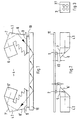
- the device shown in FIG. 1 has a radiation conductor 4 with a with respect to the beam path on the input side section 4.1 and a section 4.2 on the output side.
- the input section 4.1 and the output-side section 4.2 are opposite each other via a silicone cushion 10 the outside of the disc 11 coupled to this, so that the (by means of Arrows marked) beam path through the inside of the disc 10 in Area between the input section 4.1 and that thereof spaced output-side section 4.2 through the interior of the disk 11 runs.
- the radiation guide 4 also has the first for guiding the beam Deflection surfaces 7, 8 and second deflection surfaces 8 ', 7' with which the beam 1 is deflected in the plane of the drawing.
- Fig. 2 shows a plan view. 2 is parallel to that a circuit board 12 is arranged at the rear level of the radiation conductor 4, on which a transmitter 1 and a receiver 2, in the present case using SMD technology, are upset.
- the transmitter at a relatively short distance x2 is a beam entry surface 3 of the input section 4.1 arranged opposite, while the receiver 2 also in relative a small exit x1 opposite a beam exit surface of the output-side section 4.2 is arranged.
- the one from transmitter 1 emitted beam is at the at an angle of 45 ° to the plane of Circuit board 12 oriented input-side deflection surface 6 under right Angle directed into the radiation conductor 4 so that it, as shown in Fig. 1, by this parallel to the level of the circuit board 12 to the output side Deflection surface 6 'is performed, which is also at an angle of 45 ° to the plane the circuit board 12 is oriented.
- the one on the output side Deflection surface 6 'deflected at right angles passes over the Beam exit surface 5 on the correspondingly positioned receiver 2.
- Beam entry surface 3 is designed as an outwardly curved converging lens, and the beam exit surface 5 is also a convex lens that is curved outwards designed to completely emit the radiation leaving the radiation conductor 4 to lead the receiver 2. Often those are made using SMD technology Transmitter 1 is relatively small, so that it is cheap to increase in the Radiation conductor 4 coupled radiation power several, e.g. four Apply transmitter elements.
- the beam entry surface 3 can then, as in Fig. 3, lens elements 3.1 assigned to the individual transmitter elements which have a size corresponding to the emitted beam, Curvature and distance from the transmitter 1 are formed and arranged.
- the output-side deflection surface 6 ' can be fitted with corresponding lens elements such as the input-side deflection surface 6 may be provided.
- the output-side deflection surface 6 ' can be fitted with corresponding lens elements such as the input-side deflection surface 6 may be provided.
- they are in SMD technology available receivers in the form of photodiodes in their Dimensions larger than the transmitter designed as transmitter diodes 1.
- the jet exit surface 5 in this and in other cases advantageous to design the converging lens as a Fresnel lens, so that overall a relatively flat structure despite a relatively large curvature and Collective property or bundle property results.
- the Beam entry surface 3 can be designed as a Fresnel lens structure. All Lenses can be spherically shaped to simplify manufacture, because accurate imaging properties are less important than one uniform, controllable lighting.
- the design and arrangement of the transmitter 1 and the receiver 2 in SMD technology leaves a simple assembly of the circuit board in the same Work step in which the other components are also applied.
- the positioning and alignment of the transmitter 1 and the receiver 2 always very accurate, so that no additional measures in this regard required are. Also results from the arrangement and relatively small Dimensions of the transmitter 1 and the receiver 2 more space on the Circuit board 12 and a cheaper positioning option for others electrical components used for signal processing. It has shown, that the measures described allow only a circuit board to use the dimensions of the outer dimensions of the Radiation conductor corresponds.
Landscapes
- Engineering & Computer Science (AREA)
- Automation & Control Theory (AREA)
- Mechanical Engineering (AREA)
- Chemical & Material Sciences (AREA)
- Health & Medical Sciences (AREA)
- Life Sciences & Earth Sciences (AREA)
- Physics & Mathematics (AREA)
- Analytical Chemistry (AREA)
- Biochemistry (AREA)
- General Health & Medical Sciences (AREA)
- General Physics & Mathematics (AREA)
- Immunology (AREA)
- Pathology (AREA)
- Photometry And Measurement Of Optical Pulse Characteristics (AREA)
- Investigating Or Analysing Materials By Optical Means (AREA)
Description
- Fig. 1
- eine Vorderansicht der Vorrichtung zum Erfassen von Benetzungsereignissen auf einer Scheibe in einem an die Scheibe angekoppelten Zustand
- Fig. 2
- die Vorrichtung gemäß Fig. 1 in Draufsicht und
- Fig. 3
- eine Strahleintritts- oder Strahlaustrittsfläche mit mehreren einzelnen Linsenelementen.
Claims (10)
- Vorrichtung zum Erfassen von Benetzungsereignissen auf einer Scheibe (11), insbesondere Windschutzscheibe eines Kraftfahrzeugs, mit einer mindestens einen Sender (1) aufweisenden Strahlungssendereinrichtung, mit einem an der Scheibe (11) ankoppelbaren Strahlungsleiter (4), der zum Aufnehmen der abgesandten Strahlung eine Strahleintrittsfläche (3) und zum Abgeben der Strahlung eine Strahlaustrittsfläche (5) aufweist, und mit einer die austretende Strahlung aufnehmenden Strahlungsempfängereinrichtung, die mindestens einen Empfänger (2) aufweist, wobei der Sender (1) und der Empfänger (2) auf einer Schaltungsplatine (12) aufgebracht sind, und der Strahlungsleiter (4) annähernd parallel zu der Schaltungsplatine (12) ausgerichtet ist, und die Strahleintrittsfläche (3) und/oder die Strahlaustrittsfläche (5) auf der der Schaltungsplatine (12) zugewandten parallelen Seite des Strahlungsleiters (4) angeordnet ist/sind, und die optische Achse des Senders (1) oder Empfängers (2) senkrecht zu der Strahleintrittsfläche (3) oder der Strahlaustrittsfläche (5) ausgerichtet sind, und der Strahlungsleiter (4) zumindest eine eingangsseitige oder ausgangsseitige Ablenkfläche (6, 6') aufweist, mit der die in den Strahlungsleiter (4) eingetretene Strahlung rechtwinklig in das Innere des Strahlungsleiters (4) oder die aus dem Strahlungsleiter (4) heraus auf den Empfänger (2) zu richtende Strahlung rechtwinklig aus dem Innern des Strahlungsleiters (4) geführt wird, dadurch gekennzeichnet, daß der Strahlungsleiter (4) mehrere Umlenkflächen (7, 8, 7', 8') aufweist, mit denen die abgegebene Strahlung in einem eingangsseitigen Abschnitt (4.1) in die Scheibe (11) und die von der Scheibe (11) kommende Strahlung in einem ausgangsseitigen Abschnitt (4.2) auf die ausgangsseitige Ablenkfläche (6') geführt wird und daß mindestens eine der Umlenkflächen (7, 8, 7', 8') und/oder mindestens eine der Ablenkflächen (6, 6') zum Konvergieren oder Divergieren der Strahlung konvex nach außen oder konkav nach innen gekrümmt ist, wobei eine Spiegelung durch Totalrefelexion erhalten bleibt.
- Vorrichtung zum Erfassen von Benetzungsereignissen auf einer Scheibe, insbesondere einer Windschutzscheibe eines Kraftfahrzeugs, mit einer mindestens einen Sender aufweisenden Strahlungssendereinrichtung, mit einem an der Scheibe ankoppelbaren Strahlungsleiter, der zum Aufnehmen der abgesandten Strahlung eine Strahleintrittsfläche aufweist, und mit einer die austretende Strahlung aufnehmenden Strahlungsempfängereinrichtung, die mindestens einen Empfänger aufweist, wobei der Strahlungsleiter (4) zumindest eine eingangsseitige bzw. ausgangsseitige Ablenkfläche (6, 6') aufweist, mit der die in den Strahlungsleiter (4) eingetretene Strahlung rechtwinklig in das Innere des Strahlungsleiters (4) bzw. aus dem Strahlungsleiter (4) heraus auf den Empfänger (2) zu richtende Strahlung rechtwinklig aus dem Inneren des Strahlungsleiters geführt ist, dadurch gekennzeichnet, dass der Strahlungsleiter (4) mehrere Umlenkflächen (7, 8, 7', 8') aufweist, mit denen die abgegebene Strahlung in einem eingangsseitigen Abschnitt (4.1) in die Scheibe (11) und die von der Scheibe (11) kommende Strahlung in einem ausgangsseitigen Abschnitt (4.2) auf die ausgangsseitige Ablenkfläche (6') geführt wird und dass mindestens eine der Umlenkflächen (7, 8, 7',8') und/oder mindestens eine der Ablenkflächen (6, 6') zum Konvergieren oder zum Divergieren der Strahlung konvex nach außen bzw. konkav nach innen gekrümmt ist, wobei eine Spiegelung durch Totalreflexion erhalten bleibt.
- Vorrichtung nach Anspruch 1, dadurch gekennzeichnet, daß der mindestens eine Sender (1) und der mindestens eine Empfänger (2) als SMD-Bauelemente ausgebildet sind.
- Vorrichtung nach Anspruch 2, dadurch gekennzeichnet, daß eine Schaltungsplatine (12) vorgesehen ist und der mindestens eine Sender (1) und der mindestens eine Empfänger (2) als SMD-Bauelemente ausgebildet sind.
- Vorrichtung nach einem der vorhergehenden Ansprüche, dadurch gekennzeichnet, daß die Strahleintrittsfläche (3) und/oder die Strahlaustrittsfläche (5) als Sammellinsen ausgebildet sind.
- Vorrichtung nach Anspruch 5, dadurch gekennzeichnet, daß die Sammellinsen der Strahleintritts- (3) und der Strahlaustrittsfläche (5) als Fresnellinsen oder als mehrere einzelne auf einer ebenen Fläche angeordnete Linsenelemente (3.1) ausgebildet sind oder dass die Strahleintritts- (3) und die Strahlaustrittsfläche (5) wechselseitig unterschiedlich mit diesen beiden Arten der Sammellinsen versehen sind.
- Vorrichtung nach mindestens einem der Ansprüche 1, 3 bis 6, dadurch gekennzeichnet, dass die Ablenkflächen (6, 6') auf der von der Schaltungsplatine (12) abgelegenen Seite des Strahlungsleiters (4) vorgesehen und bei Draufsicht auf die lange Schmalseite der Schaltungsplatine (12) unter einem Winkel von 45 Grad zur Ebene der Schaltungsplatine (12) geneigt sind.
- Vorrichtung nach mindestens einem der vorhergehenden Ansprüche, dadurch gekennzeichnet, dass die Krümmung torisch ist.
- Vorrichtung nach einem der vorhergehenden Ansprüche, dadurch gekennzeichnet, dass mehrere Sender (1) vorgesehen sind, denen auf einer Strahleintrittsfläche (3) jeweils ein separates Linsenelement (3.1) zugeordnet ist und dass ein Empfänger (2) vorgesehen ist, dem auf der Strahlaustrittsfläche (5) eine Fresnellinse zugeordnet ist.
- Vorrichtung nach einem der Ansprüche 5 bis 9, dadurch gekennzeichnet, dass die Sammellinsen sphärisch ausgebildet sind.
Applications Claiming Priority (3)
| Application Number | Priority Date | Filing Date | Title |
|---|---|---|---|
| DE19608648 | 1996-03-06 | ||
| DE19608648A DE19608648C1 (de) | 1996-03-06 | 1996-03-06 | Vorrichtung zum Erfassen von Benetzungsereignissen auf einer Scheibe |
| PCT/DE1997/000335 WO1997032762A1 (de) | 1996-03-06 | 1997-02-26 | Vorrichtung zum erfassen von benetzungsereignissen auf einer scheibe |
Publications (2)
| Publication Number | Publication Date |
|---|---|
| EP0833764A1 EP0833764A1 (de) | 1998-04-08 |
| EP0833764B1 true EP0833764B1 (de) | 2003-07-09 |
Family
ID=7787386
Family Applications (1)
| Application Number | Title | Priority Date | Filing Date |
|---|---|---|---|
| EP97915303A Expired - Lifetime EP0833764B1 (de) | 1996-03-06 | 1997-02-26 | Vorrichtung zum erfassen von benetzungsereignissen auf einer scheibe |
Country Status (6)
| Country | Link |
|---|---|
| US (1) | US6064059A (de) |
| EP (1) | EP0833764B1 (de) |
| JP (1) | JP3916668B2 (de) |
| DE (2) | DE19608648C1 (de) |
| ES (1) | ES2203794T3 (de) |
| WO (1) | WO1997032762A1 (de) |
Cited By (1)
| Publication number | Priority date | Publication date | Assignee | Title |
|---|---|---|---|---|
| DE202006000742U1 (de) * | 2006-01-18 | 2007-05-24 | Trw Automotive Electronics & Components Gmbh & Co. Kg | Optische Sensorvorrichtung |
Families Citing this family (12)
| Publication number | Priority date | Publication date | Assignee | Title |
|---|---|---|---|---|
| US5661303A (en) * | 1996-05-24 | 1997-08-26 | Libbey-Owens-Ford Co. | Compact moisture sensor with collimator lenses and prismatic coupler |
| DE19946220C1 (de) * | 1999-09-22 | 2001-01-04 | Jenoptik Jena Gmbh | Optoelektronische Sensoreinrichtung |
| AU2001256696A1 (en) * | 2000-05-12 | 2001-11-20 | Nippon Sheet Glass Co. Ltd. | Adhering substance detector and controller using the same |
| DE202006005665U1 (de) * | 2006-04-05 | 2007-08-16 | Trw Automotive Electronics & Components Gmbh & Co. Kg | Optische Sensorvorrichtung |
| DE102007025987A1 (de) | 2007-06-04 | 2009-01-08 | Trw Automotive Electronics & Components Gmbh | Optische Sensorvorrichtung zur Erfassung einer Benetzung |
| DE102007036492B4 (de) | 2007-08-01 | 2009-07-30 | Trw Automotive Electronics & Components Gmbh & Co. Kg | Optische Sensorvorrichtung |
| DE102007039349A1 (de) * | 2007-08-01 | 2009-02-05 | Robert Bosch Gmbh | Vorrichtung zur Bestimmung der Reflexionseigenschaften einer Grenzfläche |
| DE102008020171B4 (de) | 2008-04-22 | 2010-08-05 | Trw Automotive Electronics & Components Gmbh | Optische Sensorvorrichtung |
| DE102008023845B4 (de) | 2008-05-16 | 2018-04-05 | Trw Automotive Electronics & Components Gmbh | Optische Sensorvorrichtung zur Detektion von Umgebungslicht |
| DE102009053825A1 (de) | 2009-11-18 | 2011-05-19 | Trw Automotive Electronics & Components Gmbh | Optische Sensorvorrichtung zur Detektion von Umgebungslicht |
| JP5761143B2 (ja) * | 2011-11-02 | 2015-08-12 | 株式会社リコー | 撮像ユニット、撮像ユニットを搭載した車両 |
| DE102018119412B4 (de) * | 2018-08-09 | 2023-03-30 | Bcs Automotive Interface Solutions Gmbh | Optische Baugruppe sowie Verfahren zur Herstellung einer optischen Baugruppe |
Family Cites Families (13)
| Publication number | Priority date | Publication date | Assignee | Title |
|---|---|---|---|---|
| JPS59152447U (ja) * | 1983-03-31 | 1984-10-12 | 株式会社東海理化電機製作所 | 雨滴センサ |
| JPS59152446U (ja) * | 1983-03-31 | 1984-10-12 | 株式会社東海理化電機製作所 | 雨滴センサ |
| US4676638A (en) * | 1983-03-31 | 1987-06-30 | Kabushiki Kaisha Tokai Rika Denki Seisakusho | Light-transmissible foreign object sensor |
| JPS61116645A (ja) * | 1984-11-09 | 1986-06-04 | Nippon Denso Co Ltd | ウインドシ−ルドワイパ自動制御装置のための液体検出器 |
| US4652745A (en) * | 1985-12-06 | 1987-03-24 | Ford Motor Company | Optical moisture sensor for a window or windshield |
| DE3806881A1 (de) * | 1988-03-03 | 1989-09-07 | Kostal Leopold Gmbh & Co Kg | Sensoreinrichtung |
| US5263111A (en) * | 1991-04-15 | 1993-11-16 | Raychem Corporation | Optical waveguide structures and formation methods |
| US5414257A (en) * | 1991-04-23 | 1995-05-09 | Introlab Pty Limited | Moisture sensor for detecting moisture on a windshield |
| DE4202121C1 (en) * | 1992-01-27 | 1992-12-24 | Leopold Kostal Gmbh & Co Kg, 5880 Luedenscheid, De | Sensor assembly detecting wetness of motor vehicle windscreen - includes receiver for radiation reflected from precipitation esp. drops of rain |
| DE4329609C1 (de) * | 1993-09-02 | 1995-02-02 | Kostal Leopold Gmbh & Co Kg | Optoelektronische Sensoreinrichtung |
| DE4406398A1 (de) * | 1994-02-26 | 1995-08-31 | Bosch Gmbh Robert | Regensensor |
| DE4410217C2 (de) * | 1994-03-24 | 2003-12-11 | Bosch Gmbh Robert | Befestigung und Ankopplung eines opto-elektronischen Sensors an einer Scheibe sowie Aufbau des Sensors |
| US5661303A (en) * | 1996-05-24 | 1997-08-26 | Libbey-Owens-Ford Co. | Compact moisture sensor with collimator lenses and prismatic coupler |
-
1996
- 1996-03-06 DE DE19608648A patent/DE19608648C1/de not_active Revoked
-
1997
- 1997-02-26 EP EP97915303A patent/EP0833764B1/de not_active Expired - Lifetime
- 1997-02-26 US US08/945,823 patent/US6064059A/en not_active Expired - Fee Related
- 1997-02-26 ES ES97915303T patent/ES2203794T3/es not_active Expired - Lifetime
- 1997-02-26 WO PCT/DE1997/000335 patent/WO1997032762A1/de not_active Ceased
- 1997-02-26 JP JP53132597A patent/JP3916668B2/ja not_active Expired - Fee Related
- 1997-02-26 DE DE59710407T patent/DE59710407D1/de not_active Expired - Lifetime
Cited By (1)
| Publication number | Priority date | Publication date | Assignee | Title |
|---|---|---|---|---|
| DE202006000742U1 (de) * | 2006-01-18 | 2007-05-24 | Trw Automotive Electronics & Components Gmbh & Co. Kg | Optische Sensorvorrichtung |
Also Published As
| Publication number | Publication date |
|---|---|
| DE19608648C1 (de) | 1997-10-23 |
| DE59710407D1 (de) | 2003-08-14 |
| JP3916668B2 (ja) | 2007-05-16 |
| JPH11505030A (ja) | 1999-05-11 |
| EP0833764A1 (de) | 1998-04-08 |
| US6064059A (en) | 2000-05-16 |
| WO1997032762A1 (de) | 1997-09-12 |
| ES2203794T3 (es) | 2004-04-16 |
Similar Documents
| Publication | Publication Date | Title |
|---|---|---|
| EP0833764B1 (de) | Vorrichtung zum erfassen von benetzungsereignissen auf einer scheibe | |
| DE69129817T2 (de) | Optische Vorrichtung | |
| DE2648604C3 (de) | Linse für einen Lichtsender in einem Fernsteuersystem | |
| EP2120025B1 (de) | Optische Sensorvorrichtung zur Detektion von Umgebungslicht | |
| DE69611282T2 (de) | Optische Unteranordnung mit niedriger Abmessung | |
| DE60224342T2 (de) | Bidirektionale optische Übertragungsvorrichtung | |
| EP0706069A1 (de) | Sende- und Empfangsmodul für eine bidirektionale optische Nachrichten- und Signalübertragung | |
| CH668490A5 (de) | Optischer multiplexer/demultiplexer. | |
| EP1813487A1 (de) | Optische Sensorvorrichtung | |
| DE112019000511B4 (de) | Lidar-vorrichtung | |
| DE19834090A1 (de) | Optoelektronische Sende- und Empfangseinheit | |
| DE69213778T2 (de) | Verfahren zur Herstellung eines opto-elektronischen Bauteils | |
| DE69015588T2 (de) | Optischer Kopf integrierbar in einem hybriden Schaltkreis. | |
| EP0790678A2 (de) | Anordnung zur optischen Ankopplung einer Monitordiode an eine Laserdiode | |
| DE3235253A1 (de) | Optisches kopplernetzwerk zum verkoppeln von mehreren teilnehmersendern mit mehreren teilnehmerempfaengern mittels optischer sternkoppler | |
| EP1653265B1 (de) | Anordnung zur optischen Kopplung eines Lichtwellenleiters mit einer optischen Einheit eines optischen Moduls sowie Koppelelement für eine solche Anordnung | |
| DE3807077C2 (de) | ||
| DE19810624A1 (de) | Elektrooptisches Modul | |
| EP1591813B1 (de) | Verfahren zur Ausrichtung eines Lichtwellenleiters in Bezug auf eine optische Einheit eines optischen Moduls, optisches Modul und Bausatz mit einem optischen Modul | |
| DE19718949A1 (de) | Elektrooptisches Modul | |
| DE102017218259B4 (de) | Halbleiter-Lichtempfangsmodul | |
| DE4445997C2 (de) | Anordnung zur Ankopplung einer Lichtleitfaser an ein optisches Bauelement | |
| EP0420029A1 (de) | Einrichtung zur Umlenkung und Fokussierung eines Lichtstrahls | |
| EP0622874A1 (de) | Anordnung zur Ankopplung eines optoelektronischen Empfangselementes an ein optoelektronisches Sendeelement | |
| DE29623536U1 (de) | Vorrichtung zum Erfassen von Benetzungsereignissen auf einer Scheibe |
Legal Events
| Date | Code | Title | Description |
|---|---|---|---|
| PUAI | Public reference made under article 153(3) epc to a published international application that has entered the european phase |
Free format text: ORIGINAL CODE: 0009012 |
|
| AK | Designated contracting states |
Kind code of ref document: A1 Designated state(s): DE ES FR GB IT SE |
|
| 17P | Request for examination filed |
Effective date: 19980312 |
|
| 17Q | First examination report despatched |
Effective date: 20010124 |
|
| GRAH | Despatch of communication of intention to grant a patent |
Free format text: ORIGINAL CODE: EPIDOS IGRA |
|
| GRAH | Despatch of communication of intention to grant a patent |
Free format text: ORIGINAL CODE: EPIDOS IGRA |
|
| GRAA | (expected) grant |
Free format text: ORIGINAL CODE: 0009210 |
|
| AK | Designated contracting states |
Designated state(s): DE ES FR GB IT SE |
|
| REG | Reference to a national code |
Ref country code: GB Ref legal event code: FG4D Free format text: NOT ENGLISH |
|
| REF | Corresponds to: |
Ref document number: 59710407 Country of ref document: DE Date of ref document: 20030814 Kind code of ref document: P |
|
| REG | Reference to a national code |
Ref country code: SE Ref legal event code: TRGR |
|
| GBT | Gb: translation of ep patent filed (gb section 77(6)(a)/1977) |
Effective date: 20031031 |
|
| ET | Fr: translation filed | ||
| REG | Reference to a national code |
Ref country code: ES Ref legal event code: FG2A Ref document number: 2203794 Country of ref document: ES Kind code of ref document: T3 |
|
| PLBE | No opposition filed within time limit |
Free format text: ORIGINAL CODE: 0009261 |
|
| STAA | Information on the status of an ep patent application or granted ep patent |
Free format text: STATUS: NO OPPOSITION FILED WITHIN TIME LIMIT |
|
| 26N | No opposition filed |
Effective date: 20040414 |
|
| PGFP | Annual fee paid to national office [announced via postgrant information from national office to epo] |
Ref country code: ES Payment date: 20080221 Year of fee payment: 12 |
|
| PGFP | Annual fee paid to national office [announced via postgrant information from national office to epo] |
Ref country code: IT Payment date: 20080228 Year of fee payment: 12 Ref country code: GB Payment date: 20080222 Year of fee payment: 12 |
|
| GBPC | Gb: european patent ceased through non-payment of renewal fee |
Effective date: 20090226 |
|
| REG | Reference to a national code |
Ref country code: ES Ref legal event code: FD2A Effective date: 20090227 |
|
| PG25 | Lapsed in a contracting state [announced via postgrant information from national office to epo] |
Ref country code: GB Free format text: LAPSE BECAUSE OF NON-PAYMENT OF DUE FEES Effective date: 20090226 |
|
| PG25 | Lapsed in a contracting state [announced via postgrant information from national office to epo] |
Ref country code: ES Free format text: LAPSE BECAUSE OF NON-PAYMENT OF DUE FEES Effective date: 20090227 |
|
| PG25 | Lapsed in a contracting state [announced via postgrant information from national office to epo] |
Ref country code: IT Free format text: LAPSE BECAUSE OF NON-PAYMENT OF DUE FEES Effective date: 20090226 |
|
| PGFP | Annual fee paid to national office [announced via postgrant information from national office to epo] |
Ref country code: SE Payment date: 20110221 Year of fee payment: 15 |
|
| PGFP | Annual fee paid to national office [announced via postgrant information from national office to epo] |
Ref country code: FR Payment date: 20120228 Year of fee payment: 16 |
|
| PGFP | Annual fee paid to national office [announced via postgrant information from national office to epo] |
Ref country code: DE Payment date: 20120423 Year of fee payment: 16 |
|
| PG25 | Lapsed in a contracting state [announced via postgrant information from national office to epo] |
Ref country code: SE Free format text: LAPSE BECAUSE OF NON-PAYMENT OF DUE FEES Effective date: 20120227 |
|
| REG | Reference to a national code |
Ref country code: FR Ref legal event code: ST Effective date: 20131031 |
|
| REG | Reference to a national code |
Ref country code: DE Ref legal event code: R119 Ref document number: 59710407 Country of ref document: DE Effective date: 20130903 |
|
| PG25 | Lapsed in a contracting state [announced via postgrant information from national office to epo] |
Ref country code: FR Free format text: LAPSE BECAUSE OF NON-PAYMENT OF DUE FEES Effective date: 20130228 Ref country code: DE Free format text: LAPSE BECAUSE OF NON-PAYMENT OF DUE FEES Effective date: 20130903 |