EP0831480B1 - Appareil et procédé de traitement d'information - Google Patents
Appareil et procédé de traitement d'information Download PDFInfo
- Publication number
- EP0831480B1 EP0831480B1 EP96306941A EP96306941A EP0831480B1 EP 0831480 B1 EP0831480 B1 EP 0831480B1 EP 96306941 A EP96306941 A EP 96306941A EP 96306941 A EP96306941 A EP 96306941A EP 0831480 B1 EP0831480 B1 EP 0831480B1
- Authority
- EP
- European Patent Office
- Prior art keywords
- signal
- gain control
- region
- output
- gain
- Prior art date
- Legal status (The legal status is an assumption and is not a legal conclusion. Google has not performed a legal analysis and makes no representation as to the accuracy of the status listed.)
- Expired - Lifetime
Links
Images
Classifications
-
- G—PHYSICS
- G11—INFORMATION STORAGE
- G11B—INFORMATION STORAGE BASED ON RELATIVE MOVEMENT BETWEEN RECORD CARRIER AND TRANSDUCER
- G11B15/00—Driving, starting or stopping record carriers of filamentary or web form; Driving both such record carriers and heads; Guiding such record carriers or containers therefor; Control thereof; Control of operating function
- G11B15/02—Control of operating function, e.g. switching from recording to reproducing
- G11B15/05—Control of operating function, e.g. switching from recording to reproducing by sensing features present on or derived from record carrier or container
- G11B15/087—Control of operating function, e.g. switching from recording to reproducing by sensing features present on or derived from record carrier or container by sensing recorded signals
-
- G—PHYSICS
- G11—INFORMATION STORAGE
- G11B—INFORMATION STORAGE BASED ON RELATIVE MOVEMENT BETWEEN RECORD CARRIER AND TRANSDUCER
- G11B20/00—Signal processing not specific to the method of recording or reproducing; Circuits therefor
- G11B20/10—Digital recording or reproducing
- G11B20/10009—Improvement or modification of read or write signals
-
- G—PHYSICS
- G11—INFORMATION STORAGE
- G11B—INFORMATION STORAGE BASED ON RELATIVE MOVEMENT BETWEEN RECORD CARRIER AND TRANSDUCER
- G11B5/00—Recording by magnetisation or demagnetisation of a record carrier; Reproducing by magnetic means; Record carriers therefor
- G11B5/02—Recording, reproducing, or erasing methods; Read, write or erase circuits therefor
- G11B5/027—Analogue recording
- G11B5/035—Equalising
-
- H—ELECTRICITY
- H03—ELECTRONIC CIRCUITRY
- H03G—CONTROL OF AMPLIFICATION
- H03G3/00—Gain control in amplifiers or frequency changers without distortion of the input signal
- H03G3/20—Automatic control
- H03G3/30—Automatic control in amplifiers having semiconductor devices
-
- G—PHYSICS
- G11—INFORMATION STORAGE
- G11B—INFORMATION STORAGE BASED ON RELATIVE MOVEMENT BETWEEN RECORD CARRIER AND TRANSDUCER
- G11B20/00—Signal processing not specific to the method of recording or reproducing; Circuits therefor
- G11B20/10—Digital recording or reproducing
- G11B2020/1087—Digital recording or reproducing wherein a selection is made among at least two alternative ways of processing
- G11B2020/10888—Digital recording or reproducing wherein a selection is made among at least two alternative ways of processing the kind of data being the selection criterion
-
- G—PHYSICS
- G11—INFORMATION STORAGE
- G11B—INFORMATION STORAGE BASED ON RELATIVE MOVEMENT BETWEEN RECORD CARRIER AND TRANSDUCER
- G11B5/00—Recording by magnetisation or demagnetisation of a record carrier; Reproducing by magnetic means; Record carriers therefor
- G11B5/008—Recording on, or reproducing or erasing from, magnetic tapes, sheets, e.g. cards, or wires
- G11B5/00813—Recording on, or reproducing or erasing from, magnetic tapes, sheets, e.g. cards, or wires magnetic tapes
Definitions
- This invention relates to data processing apparatus and methods, and to electronic circuits for use in connection therewith.
- the invention relates to apparatus and methods for retrieving data stored using a DDS Data Storage System.
- the invention also extends in general to apparatus and methods for processing data in one or more communications channels.
- DDS Digital Data Storage
- data are recorded on an elongate recording media, comprising a tape coated with a magnetic medium, by a rotating drum carrying one or more electro-magnetic heads.
- the tape is moved by a motor-driven capstan along a path extending between two spools or reels and wrapped partially around the drum.
- the plane of rotation of the heads of the drum is disposed at an angle to the plane of movement of the tape, so that each head traverses the tape along successive tracks extending across the width of the tape at an angle to its centre line.
- the mechanism includes appropriate circuitry for encoding data into signals suitable for recording onto tape, including error-detection and correction codes, and for conditioning of those signals into a form which is optimally matched to the characteristics of the recording media.
- additional circuitry is provided for detecting magnetic field variations stored on the tape, deriving corresponding signals, conditioning those signals into a form suitable for subsequent processing, decoding the encoded data and detecting and correcting errors.
- DDS-2 In a current format (DDS-2), data are recorded at a bit density of approximately 61 kilobits per inch (kbpi) (equivalent to approximately 24 kilobits per centimetre). At this bit density, a typical DDS tape cartridge can currently store up to approximately 8 gigabytes of data, using the longest practicable tape and techniques such as data compression to maximise the quantity of data the tape can accommodate. With the steadily increasing use of computer equipment and the volumes of data processed and stored by such equipment, it has become desirable to increase the capacity of a DDS tape cartridge still further.
- kbpi kilobits per inch
- DDS-3 when recorded on the longest practicable tape, is designed to provide a storage capacity of 12 gigabytes of uncompressed user data or typically 24 gigabytes of compressed user data.
- DDS-3 Because the linear bit density in DDS-3 is twice that of DDS-2, the bit spacing on the tape is approximately one half of the gap of the preferred read head. This means that the output signal from the read head, instead of varying between two discrete levels (+1,-1) will vary between three (+2,0,-2), and as such, DDS-3 will be a 3-level system.
- PRML partial-response maximum-likelihood
- Partial Response denotes a practicable Partial Response signalling scheme which only requires up to the Nyquist frequency bandwidth for data transmission, by enforcing deterministic intersymbol-interference at the detector input.
- Maximum Likelihood denotes a Maximum Likelihood Detection decoding scheme, implementing a Viterbi algorithm, which chooses the most likely sequence of output data, using a sequence of received samples, instead of just one received sample at a time.
- the approximately equalised signal is taken and is subjected to Automatic Gain Control to establish and stabilise the signal amplitudes, and then to full Adaptive Equalisation to a combined PR-1 target.
- an adaptive, sampled finite impulse response filter is used to provide a three-level PR-1 target transfer function.
- the signal undergoes analogue to digital conversion, followed by three-level Viterbi (or Maximum Likelihood) detection.
- clock information is extracted from the input signal and used to synchronise the Adaptive Equaliser, the analogue to digital converter, and the Viterbi decoder.
- the Adaptive Equalisation may instead be performed after analogue to digital conversion.
- data is stored as a series of tracks of alternate azimuth (referred to as the A track and B track respectively).
- Each end of each track is occupied by a margin region which is expendable, the front margin being followed by a preamble region, which is often indistinguishable from the margin.
- the preamble region is normally a plain sinusoidal tone and does not carry any data, but exists to enable the AGC loop and the clock recovery loop to achieve fast lock-on and also to identify the start of the main data region.
- a preamble detector controls the Adaptive Equaliser to ensure that the channels do not try to adapt the preamble or margin regions, because otherwise they will not be optimised for the data portion.
- WO89/02190 discloses an automatic gain control (AGC) system for calibrating the gain of an amplifier which includes an AGC multiplexer which provides an input to the AGC circuit.
- the AGC multiplexer operates in three different modes. In a first mode it applies a preset voltage level to the AGC circuit; in a second mode it applies a signal related to the amplifier output, and in a third mode it maintains its output.
- communications channel is used broadly to include channels of data retrieved from a recorded medium.
- the gain in the signal should not vary outside preset limits.
- the absolute gain and the relative gain in the signal is less than 1% for the Viterbi detector, although it is tolerant of slightly greater variation in absolute gain.
- the Adaptive Equaliser is not so demanding but still typically requires the offset gain to be less than 10% and the relative gain to be less than 1%.
- Certain gain control systems which use a peak detector to make a coarse adjustment of the gain and then examine individual bits to effect fine adjustment. These types of system are data driven and prone to collapse if the clock recovery is disturbed.
- a gain control system which is more robust as it does not require recovery of the clock signal. Furthermore, in a preferred system, a common simple peak detector may be used, even though the margin/preamble and main data regions have different spectral characteristics.
- an automatic gain control circuit for automatic gain control of an input signal comprising a first signal region followed by a second signal region, which circuit comprises:-
- embodiments of the automatic gain control circuit may be extended for use with signals comprising more than just two regions, to calibrate out gain steps at each transition between signal regions.
- one of said target values remains constant and the other thereof is adjusted.
- the automatic gain control circuit of this invention may be adapted to operate with two different input signals, e.g. from an A track and from a B track.
- the circuit may include means for receiving a further input signal (for example the B track) also comprising a first region and a second region, and said gain control loop may also be responsive to a respective target value for at least one of said first and second signal regions of said further input signal.
- the response of said gain control loop is preferably relatively fast compared to that of said target control means.
- the circuit preferably includes means for adjusting the response or bandwidth of the gain control loop between preset values.
- the bandwidth may be high at the start of the first signal region to achieve fast lock on, followed by medium bandwidth to allow accurate settling and then low bandwidth shortly before the second signal region.
- said first signal region may comprise a preamble or margin region
- said second region may comprise a random data region.
- the transitions between the preamble/margin region and the random data region may conveniently be detected using a preamble detector.
- the gain control loop advantageously comprises a common peak detector means for detecting peaks in both the first and second signal regions of the output from said amplifier means, although other level monitoring systems may be used.
- the invention also extends to an automatic gain control method for providing substantially continuous gain of a signal comprising a first signal region followed by a second signal region of different characteristics, which method comprises:-
- the data storage apparatus now to be described utilises a helical-scan technique for storing data in oblique tracks on a recording tape in a format similar to that used for the storage of PCM audio data according to the DATC Conference Standard (June 1987, Electronic Industries Association of Japan, Tokyo, Japan).
- the present apparatus is, however, adapted for storing computer data rather than digitised audio information.
- the apparatus includes a helical-scan tape deck in which magnetic tape passes at a pre-determined angle across a rotary head drum whilst the head drum is rotated.
- the head drum houses a pair of diametrically opposed read heads and a pair of diametrically opposed write heads at 90° to the read heads.
- these heads in use write overlapping oblique tracks across the tape, with the tracks written by one head having a positive azimuth and those written by the other head having a negative azimuth.
- the tracks are used to store data provided to the apparatus (main data) together with items of auxiliary information known as sub-codes which relate, for example, to the logical organisation of the main data, its mapping onto the tape, certain recording parameters (such as format identity, tape parameters etc.,) and tape usage history.
- the tracks also contain synchronisation bytes ("sync bytes") to enable data byte boundaries to be identified, and which are used to generate timing signals for controlling tape movement etc.
- margin regions At the beginning and end of each track are margin regions and there is a preamble block between the beginning margin and the main data area.
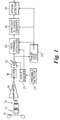
- data stored on tape 10 is read by a read-head 12 on the main drum and the signal passes via a rotary transformer 14 to an amplifier 16 and thence to a filter 18 for initial approximate equalisation to a combined PR-1 target.
- a differential signal is taken from the read head, rather than making one end grounded.
- Figure 1 shows just one signal line.
- the signal is then supplied to an automatic gain control (AGC) circuit 20 for establishing and stabilising the +2 and -2 amplitudes of the three-level signal received from the filter and integrator 18.
- AGC automatic gain control
- the signal from the AGC circuit 20 is supplied to a phase lock loop (PLL) 22 for recovery of a clock signal and is also passed to an adaptive filter referred to herein as a feed forward equaliser (FFE) 24 which provides adaptive equalisation to a combined PR-1 target, so that the overall channel frequency response matches the characteristic of an ideal PR-1 partial response channel.
- FFE feed forward equaliser
- the filtered signal is supplied to an analogue to digital converter (ADC) 26 which produces a digitised version of the filtered signal, for supply to a Viterbi detector 28.
- ADC analogue to digital converter
- the output of the Viterbi detector 28 is an NRZI-encoded data stream.
- the feed forward equaliser 24 may be located after the analogue to digital converter instead of before it.
- the automatic gain control system serves to present a constant signal amplitude to the FFE 24 to within a specified nominal amplitude.
- this amplitude must not vary along the length of any one track, or between tracks of the same azimuth.
- the variation of the amplitude of the VGA 32 during any transient behaviour of the AGC control loop must be controlled to within a pre-set relative gain error, which is much smaller than the absolute gain error.
- the recorded track comprises zones of differing spectral characteristics. The most important of these zones are the preamble regions and the random data regions.
- the AGC system when taken as a whole, must be immune to changes in frequency spectrum.
- the relative amplitude tolerance must not be exceeded on either side of the boundary between preamble regions and random data regions.
- the signal is input on lines 30 to the voltage gain amplifier (VGA) 32 and the output passes via an output driver 34 to pass onwards to the ADC 26 or FFE 28 (not shown in Figure 2).
- a feedback loop 36 comprising an amplifier 38, a low pass filter 40 and summers 42 is provided for DC offset control.
- the output from the output driver 34 also passes to a common, simple peak detector 44 which detects peaks in the output signal.
- the output of the peak detector 44 is supplied together with a target value from a digital to analogue converter (DAC) 46 to an operational transconductance amplifier (OTA) 48 which acts as a comparator.
- DAC digital to analogue converter
- OTA operational transconductance amplifier
- the output of the amplifier 48 (the VGA control voltage) is supplied to a gain control 50 which supplies the gain control signal to the VGA 32.
- the gain control loop defined by the peak detect circuit 44, amplifier 48 and gain control 50 has a relatively fast response time.
- the output of the amplifier 48 is also supplied to a pre-amplifier 52 and latching comparator 54, which tracks a measure VGA 1 of the VGA control voltage at or immediately before the interface between the preamble region and the main data region, and then holds it.
- a second measure VGA 2 of the VGA control voltage is taken a number of channel bits later (i.e. at the beginning of the main data region).
- a direct comparison of VGA 1 and VGA 2 reveals whether the gain of the voltage gain amplifier 32 has increased or decreased in making the transition between the preamble region and the random data region.
- an appropriate counter 60;62 holding the preamble target for the peak detector of the appropriate A or B track is incremented or decremented. Adjustment of the preamble target is enabled and disabled via line 64.
- a register 65 holds a constant value for the random data target for the peak detector 44 under all conditions. The response of the target control loop is slower than that of the gain control loop.
- the preamble target will have adapted to equalise the VGA control voltages immediately prior to and after the interface between the preamble region and the main data region, separately for the A and B tracks with respective target values held in counters 60 and 62, ready for the next track.
- the differing response of a simple peak detector 44 to preamble and random data is adaptively calibrated out.
- the preamble target counters 60 and 62 are saturating counters which will not overflow or underflow, and so, if one currently holds its maximum count and is asked to increment, it will maintain its maximum count. Similarly, if it holds its minimum count and is asked to decrement, it will maintain the minimum count.
- the bandwidth or response time of the target control loop may be adjusted between preset values by adjusting the bandwidth mode of the OTA amplifier 48 on line 51.
- the preamble regions of the A and B tracks exist to enable the clock recovery loop and AGC loop to achieve fast lock-up on data of known properties, and as such the regions are short.
- the bandwidth of the AGC system is selected to be high at the start of the preamble region to facilitate this fast lock-up. Once coarse amplitude settling has been achieved, medium bandwidth mode may be selected on line 51 until accurate gain amplitude settling has been achieved. Then low bandwidth mode is selected prior to the arrival of the random data so that excessive signal modulation by the VGA control voltage is avoided.
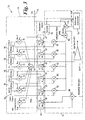
- the FFE 24 comprises a Finite Impulse Response (FIR) filter 66, a bank 68 of coefficient capacitors 69, and a circuit 70 for adapting the coefficients to reduce the error between the output on line 72 and reference values generated by reference generator 74.
- FIR Finite Impulse Response
- the signal from the AGC block 20 is input into the FIR Filter 66 on a tapped delay line 76 with delays 78 which produce in parallel successively delayed versions of the input.
- the majority of the circuit elements within the FFE 24 may be implemented in switched capacitor technology.
- the input at 76 of the FIR filter 66 is sampled by charging a capacitor at the clock time determined by the phase lock loop (PLL) 22. This charge is then passed from one capacitor to another at the bit times to form a delay line.
- the output at each stage along the delay line is multiplied at a multiplier 79 by a respective weighting coefficient from the associated coefficient capacitor 69, and all the weighted outputs are summed by summer 80 to provide the filter digital output on line 72.
- the coefficients in register 68 are repeatedly adapted to maximise the signal to noise ratio (SNR) in the equalised analogue signal on line 72, at the bit sampling times as defined by the phase lock loop 22, while the frequency response of the head and tape, or the head-tape contact conditions vary (either in manufacture or during operation).
- SNR signal to noise ratio
- the PR-1 input signal will usually be approximately spectrally shaped by the filter 18, and will consist of three levels (+2,0,-2).
- the coefficients are adapted in a least mean squares (LMS) algorithm, using an error signal which is the difference between the FIR filter output, and the nearest three level nominal signal level, provided by reference generator 74.
- the error signal is supplied in parallel to respective multipliers 82 together with the tapped and delayed input signal and this is used to adapt each of the coefficients in the coefficient capacitors 69.
- the equalised signal is monitored at 84 to determine whether it is considered to be a +2,0, or -2 signal using a reference from reference generator 74.
- the reference generator 74 supplies a slicing level signal of ⁇ 1 which the decision block 84 uses to decide whether the signal is meant to be +2, 0, or -2.
- the decision block then causes the reference generator 74 to supply the appropriate +2,0, -2 nominal level to the error summer 75 which also receives the filter output signal to obtain an error signal supplied to the multipliers 82.
- the rate of adaption may be altered between preset values (typically 6) for the signal ( ⁇ sig) and DC coefficient ( ⁇ dc), at multipliers 86 and 88.
- the FFE 24 must not be allowed to adapt in the preamble or margin regions of the A and B data tracks as it would quickly maladapt away from the optimum coefficient set for the random data region.
- the beginning and end of the main data region are normally predicted by a data recovery state machine, which uses a combination of timing and intelligent decisions based on the structure of the data on the tape and the knowledge of the format being read, relying inter-alia on the preamble detector 23 ( Figure 1).
- the preamble detector 23 may be of conventional type, typically in the form of a matched filter matched to the pure sinusoidal tone in the preamble region, and supplying a high output when the signal contains the characteristic sinusoidal tone.
- the output of the preamble detector 23 is supplied to the state machine 21, which controls the target switching for the A and B preamble and main data targets in the AGC 20, and also selection of the A and B track coefficients in the feed forward equaliser 24, as to be described below.
- the spectral characteristics of the A and B tracks differ, and the capacitors 69 store separate coefficients for the A and B tracks, with an appropriate set of coefficients being written to the FFE capacitors 69 at the beginning of each track.
- the apparatus includes a set of coefficient registers (not shown) corresponding to the coefficient capacitors 69.
- the values held on the capacitors 69 can be processed by an A-D convertor and stored in the coefficient registers.
- each track may have its own standard set of coefficients which is loaded into the coefficient capacitors at the beginning of the track, irrespective of the adapted coefficient values at the end of the previous track of that azimuth.
- the coefficient capacitors may be loaded with adapted values taken part way through the previous track of that azimuth.
- the position at which the coefficients are taken may be optimised according to machine requirements to provide the best adaption. For example if the track is curved it may be best to take coefficients from approximately half-way along the track. For any design of machine, the optimal position may be determined empirically and then production machines programmed to take the coefficients at this point. It would be possible to take the A and B coefficients at different points.
- the adapted filter coefficients from the minimum error portions of the read operations for the previous A track may be used as the initial set of coefficients for the next A track and the same process applied to the B track coefficients.
- a "snapshot timer" arrangement may be used to pick the coefficient values a predetermined time after the start of the minimum error portion of a read operation.
- successive sets of coefficients for a given A or B track may be averaged over many tracks and used as the initial set of coefficients for the next A or B track respectively.
- each of the A and B track coefficient sets there are 13 signal coefficients and one DC coefficient.
- the FFE 24 If the FFE 24 is adapting while it counters a drop out in the read signal, then the FFE coefficients can maladapt into a state from which they cannot recover. To counter this, an automatic restart mechanism is built in. When the centre coefficient falls below a programmable threshold (e.g. 50%), the coefficients are all forced to a default set of values, for example a unit step impulse response in which the centre signal coefficient is loaded with the value 1 unit and the remaining signal coefficients are forced to zero. From this starting point, the FFE 24 is allowed to continue adapting. It either maladapts again, and the process is then repeated automatically, or it converges to the correct target if the drop out contains recoverable signal.
- a programmable threshold e.g. 50%
- the centre coefficient is supplied to a comparator 90 which compares it with a value of a preset reference from reference generator 91, and implements a "kick start" routine to force the default set of coefficients if the centre coefficient has fallen below a value which, in practice, is likely to lead to the coefficients stabilising to an incorrect state.
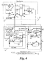
- the phase lock loop 22 is required to recover the bit clock from the read-back wave form under a variety of different conditions. Essentially, the phase lock loop 22 must acquire frequency and phase lock at the start of a track and then follow the bit frequency variations caused by head-tape velocity jitter, with a tolerable phase error.
- the phase lock loop 22 comprises a phase detector 92, a loop filter 94, and a phase accumulator 96 whose output is used to select the appropriate clock signal from a series thereof available from a system clock tapped delay line 98.
- the input signal has been subjected to automatic gain control at AGC 20, so that the nominal levels should be at 2, 0, -2 units.
- Two input comparators 100, 102 look for times when the input signal crosses a +/-1 unit (approximate) threshold. The times of these threshold crossings are then compared to the current clock time (system read clock) to determine the phase error.
- the phase error is digitally encoded (i.e. -4, -3, -2, -1, 1, 2, 3, 4 depending on the sign and magnitude of the phase error) and passed to the loop filter 94.
- the (digital) phase error is filtered using two multipliers 104, 106 and an accumulator 108.
- the phase error is multiplied by a constant, Kp.
- the phase error is multiplied by a constant Ki and the result is accumulated by the Ki accumulator 108.
- the accumulated (Ki) result and the direct (Kp) result are added together at a summer 110 and passed to the phase accumulator 96.
- the phase accumulator 96 integrates the output of the loop filter 94.
- the upper four bits of the phase accumulator output act as a "pointer" to which of the sixteen delayed versions of the external system clock available at the delay line 98 will be used as the system read clock (i.e. the clock locked to the input signal).
- phase errors build up to a large value at the output to the loop filter 94, which causes the phase accumulator 96 to increment, eventually changing the upper four bits of its output, which then selects a delayed version of the system clock which is nearer in phase to the input signal.
- the loop filter parameters are programmable; a second order loop is assumed.
- the loop bandwidth is switchable in real time, between two pre-programmed values. This is to make best use of the preamble zones, for acquisition, and still maintain low phase jitter in the data region.
- the phase lock loop 22 must be able to recover phase lock after signal drop outs that occur during normal replay of a track.
- the recovered read clock drives the FFE 24, the ADC 26 and the Viterbi decoder 28, and so must be robust. It is preferred for the phase lock loop 22 to be able to operate in DDS-1/2 or DDS-3 formats. DDS-1 or 2 format results in a two-level signal, where the bit sampling time is at the eye centre.
- the phase detector 92 typically tests for zero crossings, as this method is simple and relatively insensitive to amplitude variations.
- DDS-3 format reading of the format results in a three-level PR-1 signal.
- the phase detector 92 cannot test for simple zero crossings without disqualifying a large proportion of the incoming signal.
- a threshold crossing scheme is required (approximately +1,-1).
- the PLL 22 contains a threshold-crossing-time phase detector 92, whose output is quantised into discrete steps. In DDS-1 or 2 mode, the phase detector responds to zeros crossings, whereas in DDS-3 mode it responds to half nominal signal levels crossings.
- Figure 4 shows two (conceptual) paths through the phase detector 92, where the input signal (from the AGC 20) is compared at 100, 102 to each of the half nominal signal level threshold levels (positive and negative). The timings of the threshold crossings in the incoming signal are compared at comparator output sampler 116 with eight evenly spaced (1/8th period shifted) phases of the output clock (derived from the 16 tap delay line 98) and at the loop phase encoder 118 to the current output phase selection. The quantised phase is then determined directly by loop phase selector 120 from between which of the eight output clock phases the input crossing falls.
- DDS-1 or 2 mode the input signal is compared to a single nominal zero level reference, and only the upper (conceptual) signal path in Figure 4 is used.
- the half nominal signal thresholds are derived from phase detector threshold reference registers 112, 114, which programme DAC references to the AGC random data target DAC references. This arrangement allows the AGC targets, and PLL phase detector references to be independently optimised.
- the quantised phase output from the loop phase selector 120 is then fed to a digital loop filter 94, having a Kp (proportional) and Ki (integral) term.
- the phase detector 92 output is shown as a four bit bus (encoding the state ⁇ -4,-3,-2,-1,0,1,2,3,4 ⁇ ) and the multiplier 104,106 outputs as an eight bit bus.
- the Kp and Ki multipliers may typically have the following ranges:-
- the Ki multiplier 106 feeds the Ki accumulator 108 which in this example has a range:-
- the Ki accumulator 108 integrates the incoming Ki multiplier outputs, but only the most significant eight bits from the accumulator are added at 110 to the eight bits from the Kp multiplier 104, and then fed to the (least significant) end of the phase accumulator 96.
- the loop filter 94 can apply -252 ........ « 252 to the phase accumulator 96 per bit period.
- the two programmable pairs of Kp and Ki values are available in registers 105, 107, to give the loop a fast or slow time constant, which can be selected by a state machine, in accordance with system requirements.
- the Ki accumulator 108 is arranged to be reprogrammable when the conditions indicate that it has lost or is in danger of losing phase lock. For example, in the preamble region PLL frequency may be initialised. During so called “stunt modes" a frequency offset will occur where, for fast forward tape motion, the centre frequency of the A tracks may be displaced lower and the B tracks higher, (or vice versa for reverse tape motion). In addition, the Ki accumulator 108 may overflow either positively or negatively, indicating that the centre frequency is outside an acceptable range. Still further the Ki accumulator 108 may be re-centered if the FFE coefficients "Kickstart" routine as referred to above has been triggered. This condition indicates that there is a tape drop out or other disturbance to the signal which suggest that the PLL is likely to lose its phase lock.
- the most significant bits of the Ki accumulator 108 are loaded with the contents of a variable phase oscillator frequency offset register 109, which essentially re-centres the frequency to a default value.
- the frequency may be re-centered to that with which the PLL 22 started reading the current track.
- the digital phase accumulator 96 sums the output of the loop filter 94 and uses the four most significant bits to select an output clock phase from the sixteen tap delay line 98, which itself is phase locked to the system bit frequency clock.
- the 16 system clock phases from this delay line 98 are also used by the comparator output sampler 116 in the phase detector 92 to perform the timing of threshold crossings.
- the number of bits passed from the loop filter accumulator 108 to the phase accumulator 96 determines the maximum sustained frequency error that can be supported.
- the phase accumulator 96 integrates the loop filter 94 output (the sum of the Kp and Ki terms). The most significant four bits are used to select the phase of the system clock from the tapped delay line to be used as the current clock phase.
- the phase accumulator output 96 is represented in this example as a twelve bit number, which can be regarded as a simple unsigned up-down counter. Thus as positive loop filter outputs are applied, the accumulator counts up until it reaches 4095 and then wraps around to zero. Likewise if negative loop filter outputs are applied it counts down until it reaches zero and then wraps around to 4095. Under these conditions, the four most significant bits simply increment from 0. Vietnamese and then wrap around to zero again, to that progressively later phases of the system clock are selected as the output clock.
- the tapped delay line 98 has sixteen evenly spaced taps and is fed with the system clock.
- the delays are adjusted so that the output of the sixteenth tap is coincident with the next system clock period (where the system clock frequency is different for the various operating modes of the channel).
- a static phase offset value from a register 122 is incorporated at the summer 124 which provides an output to the clock selector 126 which selects the appropriate clock signal from the tapped delay line 98.
- the FFE 24 samples at the bit centres, whereas the PLL 22 locks to the bit edges, where the transitions are.
- phase offset register is programmed with a four bit (unsigned) number which is added to the four most significant bits of the phase accumulator to select the clock phase to be passed to the FFE 24, the ADC 26 and the rest of the system, but not the clock phase of the PLL internal clock, which is selected by the clock selector 130.
Claims (8)
- Circuit de commande automatique de gain pour la commande automatique de gain d'un signal d'entrée comprenant une première région de signal suivie par une deuxième région de signal, lequel circuit comprend :caractérisé par des moyens de commande de cible (48, 52, 54, 60, 62, 65, 46) réagissant au gain appliqué dans chacune desdites première et deuxième régions de signal pour régler au moins l'une desdites première et deuxième valeurs cibles, de façon à au moins réduire la différence entre les gains respectifs appliqués dans lesdites première et deuxième régions de signal.un moyen amplificateur de gain variable (32) destiné à recevoir et amplifier ledit signal ;une boucle de commande de gain (34, 44, 48) réagissant à la sortie dudit moyen amplificateur de gain variable (32) et à des première et deuxième valeurs cibles (60, 62, 65), pour commander le gain appliqué par ledit moyen amplificateur (32),
- Circuit de commande automatique de gain selon la revendication 1, dans lequel l'une desdites valeurs cibles reste constante et l'autre est réglée.
- Circuit de commande automatique de gain selon la revendication 1 ou la revendication 2, destiné à recevoir un autre signal d'entrée comprenant également une première région et une deuxième région, dans lequel ladite boucle de commande de gain (34, 44, 48) réagit également à une valeur cible respective pour au moins l'une desdites première et deuxième régions de signal dudit autre signal d'entrée.
- Circuit de commande automatique de gain selon l'une quelconque des revendications précédentes, dans lequel la réponse de ladite boucle de commande de gain (34, 44, 48) est relativement rapide comparée à celle desdits moyens de commande de cible.
- Circuit de commande automatique de gain selon l'une quelconque des revendications précédentes, comprenant un moyen (50) destiné à régler la réponse ou la largeur de bande de la boucle de commande de gain (34, 44, 48) entre des valeurs préétablies.
- Circuit de commande automatique de gain selon l'une quelconque des revendications précédentes, dans lequel ladite première région de signal comprend une région de préambule ou de marge, et ladite deuxième région comprend une région de données aléatoires.
- Circuit de commande automatique de gain selon l'une quelconque des revendications précédentes, dans lequel ladite boucle de commande de gain (34, 44, 48) comprend un moyen détecteur de crêtes (44) destiné à détecter des crêtes dans le signal de sortie dudit moyen amplificateur (32).
- Procédé de commande automatique de gain servant à réaliser un gain essentiellement continu sur un signal comprenant une première région de signal suivie par une deuxième région de signal ayant des caractéristiques différentes, lequel procédé comprend les opérations consistant à :caractérisé par les opérations consistant à :surveiller le gain appliqué dans une boucle de commande de gain ;prévoir des valeurs cibles respectives pour lesdites première et deuxième régions de signal,déterminer les valeurs dudit signal de commande de gain dans ladite première région de signal et ladite deuxième région de signal ; etrégler au moins l'une des valeurs cibles en fonction desdites valeurs déterminées, pour ainsi au moins réduire la différence entre les gains respectifs appliqués dans lesdites première et deuxième régions.
Priority Applications (4)
| Application Number | Priority Date | Filing Date | Title |
|---|---|---|---|
| EP96306941A EP0831480B1 (fr) | 1996-09-24 | 1996-09-24 | Appareil et procédé de traitement d'information |
| DE69620272T DE69620272T2 (de) | 1996-09-24 | 1996-09-24 | Datenverabeitungsgerät und -verfahren |
| JP25640297A JP4031559B2 (ja) | 1996-09-24 | 1997-09-22 | 入力信号の自動利得制御のための自動利得制御回路 |
| US08/934,762 US6169638B1 (en) | 1996-09-24 | 1997-09-22 | Automatic gain control circuit and method |
Applications Claiming Priority (1)
| Application Number | Priority Date | Filing Date | Title |
|---|---|---|---|
| EP96306941A EP0831480B1 (fr) | 1996-09-24 | 1996-09-24 | Appareil et procédé de traitement d'information |
Publications (2)
| Publication Number | Publication Date |
|---|---|
| EP0831480A1 EP0831480A1 (fr) | 1998-03-25 |
| EP0831480B1 true EP0831480B1 (fr) | 2001-08-08 |
Family
ID=8225096
Family Applications (1)
| Application Number | Title | Priority Date | Filing Date |
|---|---|---|---|
| EP96306941A Expired - Lifetime EP0831480B1 (fr) | 1996-09-24 | 1996-09-24 | Appareil et procédé de traitement d'information |
Country Status (4)
| Country | Link |
|---|---|
| US (1) | US6169638B1 (fr) |
| EP (1) | EP0831480B1 (fr) |
| JP (1) | JP4031559B2 (fr) |
| DE (1) | DE69620272T2 (fr) |
Cited By (4)
| Publication number | Priority date | Publication date | Assignee | Title |
|---|---|---|---|---|
| US7684291B2 (en) | 2006-06-05 | 2010-03-23 | Mediatek Inc. | Method and apparatus for blank detection of an optical disc |
| US7724090B2 (en) | 2006-06-05 | 2010-05-25 | Mediatek Inc. | Loop control apparatus and method thereof |
| US7796480B2 (en) | 2006-06-05 | 2010-09-14 | Mediatek Inc. | Apparatus and methods for light spot servo signal detection |
| CN101086854B (zh) * | 2006-06-05 | 2011-06-01 | 联发科技股份有限公司 | 回路控制装置及其方法 |
Families Citing this family (30)
| Publication number | Priority date | Publication date | Assignee | Title |
|---|---|---|---|---|
| US5976819A (en) * | 1995-11-21 | 1999-11-02 | National Jewish Medical And Research Center | Product and process to regulate actin polymerization in T lymphocytes |
| CA2239675C (fr) * | 1998-06-04 | 2007-11-13 | Tet Hin Yeap | Suppression du brouillage radioelectrique et du bruit impulsif dans les canaux de radiotelecommunications |
| US6493657B1 (en) * | 1999-08-20 | 2002-12-10 | Glp Partnership | Amplitude range matching system |
| GB2372142B (en) * | 1999-11-22 | 2003-11-12 | Seagate Technology Llc | Method and apparatus for data error recovery using defect threshold detector and viterbi gain |
| EP1146505B1 (fr) | 2000-04-10 | 2007-06-13 | Hewlett-Packard Company, A Delaware Corporation | Région du préambule d'égalisation pour le format "digital data storage" (DDS) |
| US7359132B2 (en) | 2000-04-10 | 2008-04-15 | Hewlett-Packard Development Company, L.P. | Equalization preamble region in digital data storage (DDS) format |
| TW481111U (en) * | 2001-03-30 | 2002-03-21 | Alex Machine Ind Co Ltd | Wheel set for bicycle |
| US6766153B2 (en) | 2001-04-02 | 2004-07-20 | Itran Communications Ltd. | Dynamic automatic gain control circuit employing kalman filtering |
| DE10124177A1 (de) * | 2001-05-17 | 2002-11-28 | Infineon Technologies Ag | Verfahren zur Rekonstruktion von mit einer Symbolrate getakteten Daten aus einem analogen, verzerrten Signal |
| US20030120484A1 (en) * | 2001-06-12 | 2003-06-26 | David Wong | Method and system for generating colored comfort noise in the absence of silence insertion description packets |
| US6549079B1 (en) | 2001-11-09 | 2003-04-15 | Analog Devices, Inc. | Feedback systems for enhanced oscillator switching time |
| DE50204866D1 (de) * | 2002-06-07 | 2005-12-15 | Alcatel Sa | LVSD-Treiber in bipolarer und MOS-Technologie |
| US6831510B2 (en) * | 2003-02-06 | 2004-12-14 | Fujitsu Limited | Continuous low-frequency error cancellation in a high-speed differential amplifier |
| US8223827B2 (en) | 2004-05-05 | 2012-07-17 | Agere Systems Inc. | Method and apparatus for generating filter tap weights and biases for signal dependent branch metric computation |
| GB2423218A (en) * | 2005-02-03 | 2006-08-16 | Hewlett Packard Development Co | Data storage system read/write channel optimiser which compares measured metrics of read channel with desired nominal and adjusts channel in response |
| US7030795B1 (en) * | 2005-05-17 | 2006-04-18 | Motorola, Inc. | Digital automatic gain control method and device |
| US7693674B2 (en) * | 2005-05-20 | 2010-04-06 | Omniphase Research Laboratories, Inc. | Low-noise source |
| US7295073B2 (en) * | 2006-01-19 | 2007-11-13 | Mediatek Inc. | Automatic gain control apparatus |
| WO2007111035A1 (fr) * | 2006-03-24 | 2007-10-04 | Nec Corporation | récepteur de données et circuit intégré à semiconducteurs comportant LEDIT récepteur de données |
| US7417500B2 (en) * | 2006-06-19 | 2008-08-26 | Tzero Technologies, Inc. | Control of an adjustable gain amplifier |
| US8073387B2 (en) * | 2007-05-22 | 2011-12-06 | Powerwave Technologies, Inc. | On frequency repeater with AGC stability determination |
| US7872824B1 (en) | 2007-06-11 | 2011-01-18 | Western Digital (Fremont), Llc | Setting an operating bias current for a magnetoresistive head by computing a target operating voltage |
| KR100968807B1 (ko) * | 2007-11-26 | 2010-07-08 | 한국전자통신연구원 | 가변이득증폭기 및 이를 포함하는 수신기 |
| US7760458B1 (en) * | 2008-08-12 | 2010-07-20 | Western Digital Technologies, Inc. | Disk drive adjusting head bias during servo synchronization to compensate for over/under sensitivity |
| JP2010108560A (ja) * | 2008-10-31 | 2010-05-13 | Toshiba Storage Device Corp | 信号増幅装置、記憶装置 |
| KR101544859B1 (ko) * | 2009-03-23 | 2015-08-17 | 삼성전자주식회사 | 자동 이득 제어기 및 이를 포함하는 통신 단말기 |
| JP2010251885A (ja) * | 2009-04-13 | 2010-11-04 | Panasonic Corp | Agc回路 |
| CN108063601B (zh) * | 2017-12-29 | 2021-08-27 | 上海艾为电子技术股份有限公司 | 一种自动增益控制电路及信号处理系统 |
| KR20210133799A (ko) * | 2020-04-29 | 2021-11-08 | 삼성전자주식회사 | 클럭 및 데이터 복구 장치를 포함하는 데이터 송수신 시스템 및 이의 동작방법 |
| US11153129B1 (en) * | 2020-06-01 | 2021-10-19 | International Business Machines Corporation | Feedforward equalizer with programmable roaming taps |
Citations (1)
| Publication number | Priority date | Publication date | Assignee | Title |
|---|---|---|---|---|
| JPH06244660A (ja) * | 1993-02-19 | 1994-09-02 | Toshiba Corp | 自動利得制御回路 |
Family Cites Families (10)
| Publication number | Priority date | Publication date | Assignee | Title |
|---|---|---|---|---|
| US3660821A (en) * | 1970-06-17 | 1972-05-02 | Burroughs Corp | Disc file agc circuit |
| US3879674A (en) * | 1973-12-27 | 1975-04-22 | Burroughs Corp | Automatic gain control circuit |
| EP0063935A1 (fr) * | 1981-04-24 | 1982-11-03 | Iomega Corporation | Procédé et dispositif pour positionner la tête d'une unité d'entraînement de disques |
| FR2576472B1 (fr) * | 1985-01-22 | 1988-02-12 | Alcatel Thomson Faisceaux | Procede et dispositif de commande automatique de gain d'un recepteur en acces multiple a repartition temporelle |
| JPH0691481B2 (ja) * | 1987-08-18 | 1994-11-14 | 日本電気株式会社 | Agc回路 |
| US4849711A (en) * | 1987-09-04 | 1989-07-18 | Digital Equipment Corporation | Automatic gain control system |
| US4870370A (en) * | 1988-02-19 | 1989-09-26 | Silicon Systems, Inc. | Method and apparatus for two stage automatic gain control |
| JP2672699B2 (ja) * | 1990-08-28 | 1997-11-05 | 株式会社東芝 | 磁気ディスク装置におけるagc制御装置 |
| US5463603A (en) * | 1992-03-18 | 1995-10-31 | Imp, Inc. | Computer disk drive integrated data path circuit optimized for handling both data and servo signals |
| US5467231A (en) * | 1993-02-26 | 1995-11-14 | Hewlett-Packard Company | Using recorded data for auto calibration of fixed gain of a read amplifier in a data storage device |
-
1996
- 1996-09-24 DE DE69620272T patent/DE69620272T2/de not_active Expired - Lifetime
- 1996-09-24 EP EP96306941A patent/EP0831480B1/fr not_active Expired - Lifetime
-
1997
- 1997-09-22 JP JP25640297A patent/JP4031559B2/ja not_active Expired - Fee Related
- 1997-09-22 US US08/934,762 patent/US6169638B1/en not_active Expired - Lifetime
Patent Citations (1)
| Publication number | Priority date | Publication date | Assignee | Title |
|---|---|---|---|---|
| JPH06244660A (ja) * | 1993-02-19 | 1994-09-02 | Toshiba Corp | 自動利得制御回路 |
Non-Patent Citations (1)
| Title |
|---|
| PATENT ABSTRACTS OF JAPAN vol. 018, no. 629 (P - 1637) 30 November 1994 (1994-11-30) * |
Cited By (4)
| Publication number | Priority date | Publication date | Assignee | Title |
|---|---|---|---|---|
| US7684291B2 (en) | 2006-06-05 | 2010-03-23 | Mediatek Inc. | Method and apparatus for blank detection of an optical disc |
| US7724090B2 (en) | 2006-06-05 | 2010-05-25 | Mediatek Inc. | Loop control apparatus and method thereof |
| US7796480B2 (en) | 2006-06-05 | 2010-09-14 | Mediatek Inc. | Apparatus and methods for light spot servo signal detection |
| CN101086854B (zh) * | 2006-06-05 | 2011-06-01 | 联发科技股份有限公司 | 回路控制装置及其方法 |
Also Published As
| Publication number | Publication date |
|---|---|
| JP4031559B2 (ja) | 2008-01-09 |
| US6169638B1 (en) | 2001-01-02 |
| EP0831480A1 (fr) | 1998-03-25 |
| DE69620272D1 (de) | 2002-05-02 |
| DE69620272T2 (de) | 2003-07-24 |
| JPH10112622A (ja) | 1998-04-28 |
Similar Documents
| Publication | Publication Date | Title |
|---|---|---|
| EP0831480B1 (fr) | Appareil et procédé de traitement d'information | |
| EP0831478B1 (fr) | Appareil et méthodes de traitement de données | |
| EP0831483B1 (fr) | Appareil et méthodes de traitement de données | |
| EP0831479B1 (fr) | Appareil et méthodes de traitement de données | |
| US5552942A (en) | Zero phase start optimization using mean squared error in a PRML recording channel | |
| US5978162A (en) | Synchronous read channel integrated circuit employing a channel quality circuit for calibration | |
| JP3098660B2 (ja) | クロック再生装置及びrllチャネルクロック再生方法 | |
| US6124997A (en) | Data reproducing apparatus equipped with adaptive processing circuit | |
| US5392163A (en) | Digital video signal reproducing apparatus with compression and expansion of playback time | |
| US7321531B2 (en) | Apparatus for reproducing data from optical storage medium using multiple detector | |
| EP1049090B1 (fr) | Dispositif de reproduction de donnees numeriques a vitesses multiples | |
| US5940449A (en) | Signal processing system for digital signals | |
| US6252734B1 (en) | Arrangement for reproducing a digital signal from a track on a magnetic record carrier having an equalizer filter in the form of a transconductance-capacitor filter | |
| US7362957B2 (en) | Reproducing apparatus | |
| US8615539B2 (en) | Coefficient control for filter in magnetic media read channel | |
| KR100192236B1 (ko) | 디지탈 자기기록 재생장치 | |
| US20020126749A1 (en) | Method and apparatus for enhanced timing loop for a PRML data channel | |
| EP0700042A1 (fr) | Dispositif de traitement de signaux | |
| JP3225588B2 (ja) | ディジタル信号再生回路 | |
| JP3576675B2 (ja) | 再生装置 | |
| JPH09297966A (ja) | デジタル信号再生装置 | |
| JPH0528655A (ja) | データ再生装置 | |
| JP2001014803A (ja) | 磁気ディスク装置 |
Legal Events
| Date | Code | Title | Description |
|---|---|---|---|
| PUAI | Public reference made under article 153(3) epc to a published international application that has entered the european phase |
Free format text: ORIGINAL CODE: 0009012 |
|
| AK | Designated contracting states |
Kind code of ref document: A1 Designated state(s): DE FR GB |
|
| 17P | Request for examination filed |
Effective date: 19980904 |
|
| AKX | Designation fees paid |
Free format text: AT BE CH LI |
|
| RBV | Designated contracting states (corrected) |
Designated state(s): AT BE CH LI |
|
| RBV | Designated contracting states (corrected) |
Designated state(s): DE FR GB |
|
| REG | Reference to a national code |
Ref country code: DE Ref legal event code: 8566 |
|
| 17Q | First examination report despatched |
Effective date: 19990816 |
|
| GRAG | Despatch of communication of intention to grant |
Free format text: ORIGINAL CODE: EPIDOS AGRA |
|
| GRAG | Despatch of communication of intention to grant |
Free format text: ORIGINAL CODE: EPIDOS AGRA |
|
| GRAH | Despatch of communication of intention to grant a patent |
Free format text: ORIGINAL CODE: EPIDOS IGRA |
|
| GRAH | Despatch of communication of intention to grant a patent |
Free format text: ORIGINAL CODE: EPIDOS IGRA |
|
| RAP1 | Party data changed (applicant data changed or rights of an application transferred) |
Owner name: HEWLETT-PACKARD COMPANY, A DELAWARE CORPORATION |
|
| GRAA | (expected) grant |
Free format text: ORIGINAL CODE: 0009210 |
|
| AK | Designated contracting states |
Kind code of ref document: B1 Designated state(s): DE FR GB |
|
| ET | Fr: translation filed | ||
| REG | Reference to a national code |
Ref country code: GB Ref legal event code: IF02 |
|
| REF | Corresponds to: |
Ref document number: 69620272 Country of ref document: DE Date of ref document: 20020502 |
|
| PLBE | No opposition filed within time limit |
Free format text: ORIGINAL CODE: 0009261 |
|
| STAA | Information on the status of an ep patent application or granted ep patent |
Free format text: STATUS: NO OPPOSITION FILED WITHIN TIME LIMIT |
|
| 26N | No opposition filed | ||
| PGFP | Annual fee paid to national office [announced via postgrant information from national office to epo] |
Ref country code: GB Payment date: 20090929 Year of fee payment: 14 |
|
| PGFP | Annual fee paid to national office [announced via postgrant information from national office to epo] |
Ref country code: DE Payment date: 20090929 Year of fee payment: 14 |
|
| GBPC | Gb: european patent ceased through non-payment of renewal fee |
Effective date: 20100924 |
|
| REG | Reference to a national code |
Ref country code: FR Ref legal event code: ST Effective date: 20110531 |
|
| REG | Reference to a national code |
Ref country code: DE Ref legal event code: R119 Ref document number: 69620272 Country of ref document: DE Effective date: 20110401 |
|
| PG25 | Lapsed in a contracting state [announced via postgrant information from national office to epo] |
Ref country code: DE Free format text: LAPSE BECAUSE OF NON-PAYMENT OF DUE FEES Effective date: 20110401 Ref country code: FR Free format text: LAPSE BECAUSE OF NON-PAYMENT OF DUE FEES Effective date: 20100930 |
|
| PG25 | Lapsed in a contracting state [announced via postgrant information from national office to epo] |
Ref country code: GB Free format text: LAPSE BECAUSE OF NON-PAYMENT OF DUE FEES Effective date: 20100924 |
|
| PGFP | Annual fee paid to national office [announced via postgrant information from national office to epo] |
Ref country code: FR Payment date: 20091006 Year of fee payment: 14 |