EP0831376A2 - Abtastbelichtungsverfahren sowie Maske dafür - Google Patents
Abtastbelichtungsverfahren sowie Maske dafür Download PDFInfo
- Publication number
- EP0831376A2 EP0831376A2 EP97307420A EP97307420A EP0831376A2 EP 0831376 A2 EP0831376 A2 EP 0831376A2 EP 97307420 A EP97307420 A EP 97307420A EP 97307420 A EP97307420 A EP 97307420A EP 0831376 A2 EP0831376 A2 EP 0831376A2
- Authority
- EP
- European Patent Office
- Prior art keywords
- mask
- wafer
- exposure
- scan
- moved
- Prior art date
- Legal status (The legal status is an assumption and is not a legal conclusion. Google has not performed a legal analysis and makes no representation as to the accuracy of the status listed.)
- Withdrawn
Links
Images


Classifications
-
- G—PHYSICS
- G03—PHOTOGRAPHY; CINEMATOGRAPHY; ANALOGOUS TECHNIQUES USING WAVES OTHER THAN OPTICAL WAVES; ELECTROGRAPHY; HOLOGRAPHY
- G03F—PHOTOMECHANICAL PRODUCTION OF TEXTURED OR PATTERNED SURFACES, e.g. FOR PRINTING, FOR PROCESSING OF SEMICONDUCTOR DEVICES; MATERIALS THEREFOR; ORIGINALS THEREFOR; APPARATUS SPECIALLY ADAPTED THEREFOR
- G03F7/00—Photomechanical, e.g. photolithographic, production of textured or patterned surfaces, e.g. printing surfaces; Materials therefor, e.g. comprising photoresists; Apparatus specially adapted therefor
- G03F7/70—Microphotolithographic exposure; Apparatus therefor
- G03F7/70058—Mask illumination systems
- G03F7/70075—Homogenization of illumination intensity in the mask plane by using an integrator, e.g. fly's eye lens, facet mirror or glass rod, by using a diffusing optical element or by beam deflection
-
- G—PHYSICS
- G03—PHOTOGRAPHY; CINEMATOGRAPHY; ANALOGOUS TECHNIQUES USING WAVES OTHER THAN OPTICAL WAVES; ELECTROGRAPHY; HOLOGRAPHY
- G03F—PHOTOMECHANICAL PRODUCTION OF TEXTURED OR PATTERNED SURFACES, e.g. FOR PRINTING, FOR PROCESSING OF SEMICONDUCTOR DEVICES; MATERIALS THEREFOR; ORIGINALS THEREFOR; APPARATUS SPECIALLY ADAPTED THEREFOR
- G03F7/00—Photomechanical, e.g. photolithographic, production of textured or patterned surfaces, e.g. printing surfaces; Materials therefor, e.g. comprising photoresists; Apparatus specially adapted therefor
- G03F7/20—Exposure; Apparatus therefor
-
- G—PHYSICS
- G03—PHOTOGRAPHY; CINEMATOGRAPHY; ANALOGOUS TECHNIQUES USING WAVES OTHER THAN OPTICAL WAVES; ELECTROGRAPHY; HOLOGRAPHY
- G03F—PHOTOMECHANICAL PRODUCTION OF TEXTURED OR PATTERNED SURFACES, e.g. FOR PRINTING, FOR PROCESSING OF SEMICONDUCTOR DEVICES; MATERIALS THEREFOR; ORIGINALS THEREFOR; APPARATUS SPECIALLY ADAPTED THEREFOR
- G03F7/00—Photomechanical, e.g. photolithographic, production of textured or patterned surfaces, e.g. printing surfaces; Materials therefor, e.g. comprising photoresists; Apparatus specially adapted therefor
- G03F7/70—Microphotolithographic exposure; Apparatus therefor
- G03F7/70058—Mask illumination systems
- G03F7/702—Reflective illumination, i.e. reflective optical elements other than folding mirrors, e.g. extreme ultraviolet [EUV] illumination systems
-
- G—PHYSICS
- G03—PHOTOGRAPHY; CINEMATOGRAPHY; ANALOGOUS TECHNIQUES USING WAVES OTHER THAN OPTICAL WAVES; ELECTROGRAPHY; HOLOGRAPHY
- G03F—PHOTOMECHANICAL PRODUCTION OF TEXTURED OR PATTERNED SURFACES, e.g. FOR PRINTING, FOR PROCESSING OF SEMICONDUCTOR DEVICES; MATERIALS THEREFOR; ORIGINALS THEREFOR; APPARATUS SPECIALLY ADAPTED THEREFOR
- G03F7/00—Photomechanical, e.g. photolithographic, production of textured or patterned surfaces, e.g. printing surfaces; Materials therefor, e.g. comprising photoresists; Apparatus specially adapted therefor
- G03F7/70—Microphotolithographic exposure; Apparatus therefor
- G03F7/70216—Mask projection systems
- G03F7/70358—Scanning exposure, i.e. relative movement of patterned beam and workpiece during imaging
Definitions
- This invention relates to a lithographic process for scanning a mask with exposure light such as synchrotron radiation light to transfer a pattern of the mask on to a wafer.
- the invention is concerned with a mask to be used in such process.
- the degree of integration of a microdevice such as a semiconductor device is increasing more and more, and the line width of a pattern has to be reduced more and more.
- a required line width is 0.25 micron, and, for a 1G DRAM, it is 0.18 micron.
- the overall registration precision for superposedly printing mask patterns on a wafer through lithographic transfer is 80 nm for 256M DRAM and 60 nm for 1G DRAM.
- the synchrotron radiation comprises a sheet-like slit beam.
- an X-ray reflection mirror is pivoted to scanningly deflect the radiation light relative to a mask and a wafer which are held fixed or, alternatively, the mask and the wafer are scanningly moved relative to the sheet beam which is held fixed, whereby the mask pattern is transferred to the wafer.
- Japanese Laid-Open Patent Application, Laid-Open No. 55785/1996 shows correction of mask transfer magnification, wherein synchrotron radiation is used and, during scan with exposure light, a wafer and a mask are relatively moved in a scan direction to thereby correct the transfer magnification.
- a scanning exposure method comprising the steps of: relatively scanning a mask and a wafer relative to exposure light, to transfer a pattern of the mask on to the wafer; and applying a relative speed between the mask and the wafer in a scan direction, during the scan exposure, wherein the relative speed is controlled variable.
- a mask to be used in a scanning exposure process for relatively scanning a mask with a slit beam comprising: a membrane; and a mask pattern formed on said membrane; wherein the mask pattern is formed with a predetermined distortion with respect to a scan direction, having been set in accordance with thermal distortion of the mask pattern to be caused during the scan exposure.
- a device manufacturing method for producing devices through a process based on an exposure method or an exposure mask as described above.
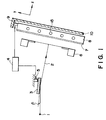
- Figure 1 is a schematic view of a main portion of an exposure apparatus according to a first embodiment of the present invention.
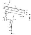
- Figure 2 is a schematic view of a main portion of an exposure apparatus according to a second embodiment of the present invention.
- Figure 3 is a schematic view of a main portion of an exposure apparatus according to a third embodiment of the present invention.
- Figure 4 is a schematic view for explaining an example of the direction and amount of pattern positional deviations, being illustrated by use of arrows.
- Figure 5 is a graph which corresponds to the characteristic of the Figure 4 example.
- Figure 6 is a schematic view for explaining another example of the direction and amount of pattern positional deviations, being illustrated by use of arrows.
- Figure 7 is a graph which corresponds to the characteristic of the Figure 6 example.
- Figure 8 is a flow chart of device manufacturing processes.
- Figure 9 is a flow chart for explaining details of a wafer process.
- FIG. 1 illustrates the structure of an exposure apparatus according to an embodiment of the present invention.
- Sheet-like exposure light (X-rays) 2 is emitted from an emission point 1 of a synchrotron ring (SR), and it is obliquely projected on an X-ray mirror 3 and is reflected thereby.
- the X-ray mirror 3 is rotated at a predetermined speed, by means of an actuator 5 which is driven in accordance with a signal from a controller 4.
- the slit-like exposure light 2 displaces along an X-ray mask 6 surface at a speed Vs, such that the whole exposure region on the mask is scanned.
- the X-ray mask 6 is held fixed, and it does not move.
- the wafer 7 is placed on a wafer chuck 8 which is mounted on a wafer stage 10 being movable both in X and Y directions, for stepwise motion between shots.
- the wafer chuck 8 is equipped with a plurality of flow passageways 15 formed therewithin, for flowing a temperature medium such as water or alcohol, for maintaining the wafer temperature constant.
- a positional deviation of the pattern of the mask with respect to the wafer, to be produced during the scan exposure can be corrected in the procedure to be described below.
- the controller 4 produces the drive signal on the basis of a data table or a calculation formula.
- Figure 6 shows another example wherein, in addition to the characteristic of Figure 4, there is a characteristic that positional deviation in Y direction becomes large in proportion to Y.
- Figure 7 shows the characteristic of this example, in graph.
- the drive speed WVy can be calculated from Dy.
- the drive speed WVy or MVy is calculated on the basis of approximating the positional deviation Dy by trigonometric function.
- the drive speed WVy or MVy may be calculated on the basis of approximating the positional deviation Dy by use of any other function.
- the pattern of the mask may be printed on one of plural shot regions on the wafer in accordance with the procedure described above. After it is completed, the wafer chuck 8 may be moved by the wafer stage 10, to a next shot region, and the same scan exposure process is repeated.
- the wafer side is moved so as to apply or produce a relative speed between a mask and a wafer during scan exposure.
- the mask side may be moved as an alternative.
- Figure 2 shows a structure that enables this.
- Calculation of the amount of correction of positional deviation may be essentially the same as that in the first embodiment.
- a rough-motion stage 10 for producing stepwise motion drive, of a large stroke is provided on the wafer side, while a Y-direction fine-motion mechanism is provided on the mask side.
- the wafer support rigidity is higher than that of the first embodiment. Therefore, vibration of the wafer chuck 8 as the temperature adjusting medium flows through the passageways 15 in the wafer chuck 8 can be reduced, and further enhancement of pattern transfer precision is attainable.
- the mask pattern is transferred to the wafer by a single scan to one picture angle.
- the exposure of one picture angle may be made with repeated scans. The following embodiment corresponds to this.
- the exposure light is moved in +Y direction of the picture angle. After the scan of the picture angle, it is shifted in +Y direction from the upper end of the picture angle of the mask. Thereafter, it is moved reversely and in -Y direction, and it is placed at the upper end of the picture angle of the mask. In the subsequent second scan, the exposure light is moved in -Y direction of the picture angle until it reaches at the lower end of the picture angle of the mask. If the time necessary for one scan is Ts, and the time from the end of first scan to the start of second scan is I, the time I is the period necessary for the reverse of the exposure light.
- the exposure light moves in +Y direction, from the upper end of the picture angle of the mask and, thereafter, it moves reversely in -Y direction and is placed again at the upper end of the picture angle of the mask.
- the second scan is performed.
- Te 2 ⁇ Ts+I.
- Dy -50sin(2 ⁇ t/Ts) nm
- the wafer may be moved at a drive speed WVy to correct this mask pattern positional deviation to thereby avoid deterioration of precision of registration with respect to the wafer.
- the controller 4 may include a data table or calculation formulae, related to the amount of drive of mirror in the positive direction and the drive speed of the wafer relative to the mask.
- the X-ray mirror is held fixed and the exposure beam is held stationary, while the mask and the wafer are moved at a speed -Vs.
- a fine-motion actuator is used to provide variable relative speed between the mask and the wafer during the scan exposure to thereby correct positional deviation of the mask pattern to the wafer.
- Figure 3 shows a structure which enables this.
- the X-ray mirror 3 is held fixed, and it does not move.
- the scan of the wafer relative to the exposure beam is performed by use of a wafer stage 10, and the scan of the mask is performed by use of a mask stage 12.
- a fine-motion actuator 9 applies a relative speed between the mask and the wafer, as has been described with reference to the embodiment explained above. Also, this relative speed is changed to correct the mask pattern deviation.
- the fine-motion actuator 9 may be mounted between mask stage 12 and mask 6.
- the relative speed of the mask and the wafer is changed to thereby correct or compensate the pattern distortion due to thermal distortion of the mask.
- correct pattern transfer can be made without relative displacement of the mask and the wafer.
- the mask pattern may be formed beforehand with a predetermined distortion with respect to the scan direction. In that occasion, if thermal distortion is produced in the mask when it is in use, the mask pattern to be transferred as a consequence to the wafer has substantially no distortion. Thus, a desired pattern can be transferred.
- the mask pattern may be designed with intentional contraction/expansion in scan direction, in accordance with distortion characteristic such as shown in Figure 4 or 6.
- Step 8 is a flow chart of procedure for manufacture of microdevices such as semiconductor chips (e.g. ICs or LSIs), liquid crystal panels or CCDs, for example.
- Step 1 is a design process for designing a circuit of a semiconductor device.
- Step 2 is a process for making a mask on the basis of the circuit pattern design.
- Step 3 is a process for preparing a wafer by using a material such as silicon.
- Step 4 is a wafer process which is called a pre-process wherein, by using the so prepared mask and wafer, circuits are practically formed on the wafer through lithography.
- Step 5 subsequent to this is an assembling step which is called a post-process wherein the wafer having been processed by step 4 is formed into semiconductor chips.
- This step includes assembling (dicing and bonding) process and packaging (chip sealing) process.
- Step 6 is an inspection step wherein operation check, durability check and so on for the semiconductor devices provided by step 5, are carried out. With these processes, semiconductor devices are completed and they are shipped (step 7).
- Step 9 is a flow chart showing details of the wafer process.
- Step 11 is an oxidation process for oxidizing the surface of a wafer.
- Step 12 is a CVD process for forming an insulating film on the wafer surface.
- Step 13 is an electrode forming process for forming electrodes upon the wafer by vapor deposition.
- Step 14 is an ion implanting process for implanting ions to the wafer.
- Step 15 is a resist process for applying a resist (photosensitive material) to the wafer.
- Step 16 is an exposure process for printing, by exposure, the circuit pattern of the mask on the wafer through the exposure apparatus described above.
- Step 17 is a developing process for developing the exposed wafer.
- Step 18 is an etching process for removing portions other than the developed resist image.
- Step 19 is a resist separation process for separating the resist material remaining on the wafer after being subjected to the etching process. By repeating these processes, circuit patterns are superposedly formed on the wafer.
Landscapes
- Physics & Mathematics (AREA)
- General Physics & Mathematics (AREA)
- Exposure And Positioning Against Photoresist Photosensitive Materials (AREA)
- Exposure Of Semiconductors, Excluding Electron Or Ion Beam Exposure (AREA)
- Electron Beam Exposure (AREA)
- Preparing Plates And Mask In Photomechanical Process (AREA)
Applications Claiming Priority (3)
| Application Number | Priority Date | Filing Date | Title |
|---|---|---|---|
| JP25162296 | 1996-09-24 | ||
| JP25162296A JPH1097976A (ja) | 1996-09-24 | 1996-09-24 | 露光方法や露光用マスク、ならびにデバイス生産方法 |
| JP251622/96 | 1996-09-24 |
Publications (2)
| Publication Number | Publication Date |
|---|---|
| EP0831376A2 true EP0831376A2 (de) | 1998-03-25 |
| EP0831376A3 EP0831376A3 (de) | 2000-04-26 |
Family
ID=17225576
Family Applications (1)
| Application Number | Title | Priority Date | Filing Date |
|---|---|---|---|
| EP97307420A Withdrawn EP0831376A3 (de) | 1996-09-24 | 1997-09-23 | Abtastbelichtungsverfahren sowie Maske dafür |
Country Status (3)
| Country | Link |
|---|---|
| US (1) | US5994003A (de) |
| EP (1) | EP0831376A3 (de) |
| JP (1) | JPH1097976A (de) |
Cited By (2)
| Publication number | Priority date | Publication date | Assignee | Title |
|---|---|---|---|---|
| US6284443B1 (en) | 1999-04-30 | 2001-09-04 | International Business Machines Corporation | Method and apparatus for image adjustment |
| EP1473598A3 (de) * | 2003-04-30 | 2005-03-09 | ASML Netherlands B.V. | Lithographischer apparat, verfahren zur herstellung einer vorrichtung und verfahren zur bestimmung einer maske und/oder einer membranabdeckung |
Families Citing this family (2)
| Publication number | Priority date | Publication date | Assignee | Title |
|---|---|---|---|---|
| CN1851557B (zh) * | 2006-06-02 | 2010-05-12 | 中国科学院光电技术研究所 | 一种二维扫描精密激光曝光系统 |
| US9529275B2 (en) * | 2007-02-21 | 2016-12-27 | Taiwan Semiconductor Manufacturing Company, Ltd. | Lithography scanner throughput |
Family Cites Families (7)
| Publication number | Priority date | Publication date | Assignee | Title |
|---|---|---|---|---|
| JPS61111532A (ja) * | 1984-11-05 | 1986-05-29 | Mitsubishi Electric Corp | X線マスク |
| JP2586662B2 (ja) * | 1989-12-07 | 1997-03-05 | 松下電器産業株式会社 | 投影露光装置 |
| US5308991A (en) * | 1992-06-02 | 1994-05-03 | National Semiconductor Corporation | Method and apparatus for making a predistorted reticle to compensate for lens distortions |
| JP3093528B2 (ja) * | 1993-07-15 | 2000-10-03 | キヤノン株式会社 | 走査型露光装置 |
| JP3101473B2 (ja) * | 1993-11-05 | 2000-10-23 | キヤノン株式会社 | 露光方法及び該露光方法を用いるデバイス製造方法 |
| US5593800A (en) * | 1994-01-06 | 1997-01-14 | Canon Kabushiki Kaisha | Mask manufacturing method and apparatus and device manufacturing method using a mask manufactured by the method or apparatus |
| JP3287725B2 (ja) * | 1994-06-07 | 2002-06-04 | キヤノン株式会社 | 露光方法とこれを用いたデバイス製造方法 |
-
1996
- 1996-09-24 JP JP25162296A patent/JPH1097976A/ja active Pending
-
1997
- 1997-09-23 EP EP97307420A patent/EP0831376A3/de not_active Withdrawn
- 1997-09-23 US US08/935,901 patent/US5994003A/en not_active Expired - Fee Related
Cited By (3)
| Publication number | Priority date | Publication date | Assignee | Title |
|---|---|---|---|---|
| US6284443B1 (en) | 1999-04-30 | 2001-09-04 | International Business Machines Corporation | Method and apparatus for image adjustment |
| EP1473598A3 (de) * | 2003-04-30 | 2005-03-09 | ASML Netherlands B.V. | Lithographischer apparat, verfahren zur herstellung einer vorrichtung und verfahren zur bestimmung einer maske und/oder einer membranabdeckung |
| US7379154B2 (en) | 2003-04-30 | 2008-05-27 | Asml Netherlands, B.V. | Lithographic apparatus, device manufacturing methods, mask and method of characterizing a mask and/or pellicle |
Also Published As
| Publication number | Publication date |
|---|---|
| EP0831376A3 (de) | 2000-04-26 |
| JPH1097976A (ja) | 1998-04-14 |
| US5994003A (en) | 1999-11-30 |
Similar Documents
| Publication | Publication Date | Title |
|---|---|---|
| EP0678768B2 (de) | Projektionsbelichtungsgerät und Herstellungsverfahren für eine Mikrovorrichtung | |
| US5995582A (en) | X-ray reduction exposure apparatus and device manufacturing method using the same | |
| US5917580A (en) | Scan exposure method and apparatus | |
| US7463335B2 (en) | Exposure apparatus, and device manufacturing method | |
| WO1993000614A1 (en) | Small field scanner | |
| US7154581B2 (en) | Scanning exposure apparatus, manufacturing method thereof, and device manufacturing method | |
| US6103433A (en) | Exposure method using reticle remount for temperature influence correction | |
| US7417715B2 (en) | Stage apparatus, lithographic apparatus and device manufacturing method using two patterning devices | |
| JP2006128699A (ja) | 調整可能な投影系を有するリソグラフィ装置およびデバイス製造方法 | |
| US7671970B2 (en) | Stage apparatus with two patterning devices, lithographic apparatus and device manufacturing method skipping an exposure field pitch | |
| US6982841B2 (en) | Mirror holding mechanism in exposure apparatus, and device manufacturing method | |
| JP2009016385A (ja) | ステージ装置、露光装置及びデバイス製造方法 | |
| JP4458329B2 (ja) | 露光装置及びデバイス製造方法 | |
| EP0833209B1 (de) | Abtastbelichtungsapparat und Verfahren zur Herstellung einer Vorrichtung unter Verwendung desselben | |
| CN1282039C (zh) | 光刻装置,器件制造方法和光学元件的制造方法 | |
| US5994003A (en) | Scanning exposure method and mask therefor | |
| JP3708075B2 (ja) | リソグラフィ装置およびデバイス製造方法 | |
| JP2005166778A (ja) | 露光装置、デバイスの製造方法 | |
| US5335259A (en) | X-ray exposure apparatus | |
| JP4719710B2 (ja) | リソグラフィ装置およびデバイス製造方法 | |
| US5596618A (en) | Exposure apparatus and device manufacturing method using the same | |
| JPH07153672A (ja) | 円柱状反射型マスク、該マスクを用いる露光方法と露光装置、これらにより製造された半導体デバイス | |
| US6078640A (en) | X-ray exposure apparatus | |
| US7060994B2 (en) | Exposure apparatus and method | |
| JP4298305B2 (ja) | 露光装置及び半導体デバイスの製造方法 |
Legal Events
| Date | Code | Title | Description |
|---|---|---|---|
| PUAI | Public reference made under article 153(3) epc to a published international application that has entered the european phase |
Free format text: ORIGINAL CODE: 0009012 |
|
| AK | Designated contracting states |
Kind code of ref document: A2 Designated state(s): DE GB NL |
|
| PUAL | Search report despatched |
Free format text: ORIGINAL CODE: 0009013 |
|
| RIC1 | Information provided on ipc code assigned before grant |
Free format text: 7G 03F 7/20 A, 7G 03F 1/14 B |
|
| AK | Designated contracting states |
Kind code of ref document: A3 Designated state(s): AT BE CH DE DK ES FI FR GB GR IE IT LI LU MC NL PT SE |
|
| 17P | Request for examination filed |
Effective date: 20000915 |
|
| AKX | Designation fees paid |
Free format text: DE GB NL |
|
| 17Q | First examination report despatched |
Effective date: 20040213 |
|
| RTI1 | Title (correction) |
Free format text: SCANNING EXPOSURE METHOD AND EXPOSURE APPARATUS THEREFOR |
|
| STAA | Information on the status of an ep patent application or granted ep patent |
Free format text: STATUS: THE APPLICATION HAS BEEN WITHDRAWN |
|
| 18W | Application withdrawn |
Effective date: 20080205 |