EP0827208A2 - Hydrogen-terminated diamond misfet and its manufacturing method - Google Patents
Hydrogen-terminated diamond misfet and its manufacturing method Download PDFInfo
- Publication number
- EP0827208A2 EP0827208A2 EP97115131A EP97115131A EP0827208A2 EP 0827208 A2 EP0827208 A2 EP 0827208A2 EP 97115131 A EP97115131 A EP 97115131A EP 97115131 A EP97115131 A EP 97115131A EP 0827208 A2 EP0827208 A2 EP 0827208A2
- Authority
- EP
- European Patent Office
- Prior art keywords
- diamond
- hydrogen
- terminated
- region
- misfet
- Prior art date
- Legal status (The legal status is an assumption and is not a legal conclusion. Google has not performed a legal analysis and makes no representation as to the accuracy of the status listed.)
- Ceased
Links
Images





Classifications
-
- H—ELECTRICITY
- H10—SEMICONDUCTOR DEVICES; ELECTRIC SOLID-STATE DEVICES NOT OTHERWISE PROVIDED FOR
- H10D—INORGANIC ELECTRIC SEMICONDUCTOR DEVICES
- H10D30/00—Field-effect transistors [FET]
- H10D30/01—Manufacture or treatment
-
- H—ELECTRICITY
- H10—SEMICONDUCTOR DEVICES; ELECTRIC SOLID-STATE DEVICES NOT OTHERWISE PROVIDED FOR
- H10D—INORGANIC ELECTRIC SEMICONDUCTOR DEVICES
- H10D30/00—Field-effect transistors [FET]
- H10D30/60—Insulated-gate field-effect transistors [IGFET]
-
- H—ELECTRICITY
- H10—SEMICONDUCTOR DEVICES; ELECTRIC SOLID-STATE DEVICES NOT OTHERWISE PROVIDED FOR
- H10D—INORGANIC ELECTRIC SEMICONDUCTOR DEVICES
- H10D62/00—Semiconductor bodies, or regions thereof, of devices having potential barriers
- H10D62/10—Shapes, relative sizes or dispositions of the regions of the semiconductor bodies; Shapes of the semiconductor bodies
- H10D62/17—Semiconductor regions connected to electrodes not carrying current to be rectified, amplified or switched, e.g. channel regions
- H10D62/213—Channel regions of field-effect devices
- H10D62/221—Channel regions of field-effect devices of FETs
- H10D62/235—Channel regions of field-effect devices of FETs of IGFETs
-
- H—ELECTRICITY
- H10—SEMICONDUCTOR DEVICES; ELECTRIC SOLID-STATE DEVICES NOT OTHERWISE PROVIDED FOR
- H10D—INORGANIC ELECTRIC SEMICONDUCTOR DEVICES
- H10D62/00—Semiconductor bodies, or regions thereof, of devices having potential barriers
- H10D62/80—Semiconductor bodies, or regions thereof, of devices having potential barriers characterised by the materials
- H10D62/83—Semiconductor bodies, or regions thereof, of devices having potential barriers characterised by the materials being Group IV materials, e.g. B-doped Si or undoped Ge
- H10D62/8303—Diamond
Definitions
- the present invention relates to a MISFET using hydrogen-terminated diamond, and to a MISFET using hydrogen-terminated diamond having elements insulated from each other, and to a method for fabricating the MISFET using hydrogen-terminated diamond.
- the present invention relates to a polycrystal diamond MISFET having a flattened hydrogen-terminated surface.
- Conventional diamond FETs are fabricated using a p-type semiconductor layer made by doping boron atoms (B) into a diamond layer (K. Kobashi, K. Nishimura, K. Miyata, R. Nakamura, H. Koyama, K. Saito and D.L. Dreifus: Proc. 2 nd Int. Conf., Appl. Of Diamond Films and Related Materials., ed. M. Yoshikawa, M. Murakawa, Y. Tzeng and W. A. Yarbrough, pp 35-42 (Saitama, 1993)).
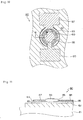
- FIG. 10 is a schematic plan view of a conventional FET mentioned above, and FIG. 11 is a fragmentary cross-sectional view taken along the B-B line of FIG. 10.
- FET 80 is made by first depositing a diamond layer 82 on a substrate 81 with no impurity doped and a boron -doped layer 83 on the diamond layer 82, then making an annular p + region 84, a circular p + region 85 concentric with the annular region 84 and an annular non-doped region 86 between the annular region 84 and the circular region 85, further making a source ohmic contact 87, a drain ohmic contact 88 or a gate electrode 89 on the respective regions. That is, this FET requires a circular geometry of elements as shown in FIG. 10 to prevent leakage of a current to the exterior, and does not suit for microminiaturization or for integration of such elements with a high density.
- LOCOS technique is used as an element insulating technique for insulating and isolating elements from each other by providing an oxide layer as shown in, for example, Japanese Patent Publication S49-45629.
- the LOCOS technique cannot be used for diamond semiconductor devices because diamond itself is not readily oxidized thick enough to form an oxide film on the surface of the diamond.
- An alternative approach for isolating elements on a diamond semiconductor device selectively removes semiconductor regions by etching, etc. to isolate respective elements on a diamond substrate as taught in, for example, "Diamond Thin-Film Recessed Gate Field-Effect Transistors Fabricated by Electron Cyclotron Resonance Plasma Etching: S. A. Grot, G. S. Gildenblat, and A. R. Badzian, IEEE ELECTRON DEVICE LETT. VOL 13 No. 9, September 1992, pp 462-463". This approach, however, requires complicated processes including etching.
- the present inventors formerly proposed at Applied Physics Conference a method for fabricating MESFET including a source ohmic contact and a drain ohmic contact made by vapor deposition of aluminum (Aoki, Ito, Kawarada, et al.: Brief of 40 th Joint Meeting Related to Applied Physics, p. 30, MK11, 12).
- This method certainly provides MESFETs having a simple structure and operative in an enhanced mode; however, since a surface conductive layer is formed directly under the hydrogen-terminated surface of the homoepitaxial diamond, even this method failed to insulate respective elements, and could not integrate a plurality of semiconductor elements on a common substrate.
- the present invention is aimed at providing a MISFET formed on the surface of a hydrogen-terminated diamond.
- the present invention is aimed at providing a simple method of manufacturing a semiconductor device wherein each element formed on the surface of the same hydrogen-terminated homoepitaxial diamond substrate with a reduced number of mask processing.
- the further object of the present invention is to provide a hydrogen-terminated diamond MISFET providing an FET having any mode of the depression mode or the enhancement mode.
- the present invention formed the hydrogen-terminated diamond MISFET mounting a drain and a source on a hydrogen-terminated region of the surface of the diamond, and a gate electrode between the drain and the source on an insulating layer.
- the present invention formed the above-mentioned hydrogen-terminated diamond MISFET wherein the diamond is formed by a homoepitaxial diamond or a heteroepitaxial diamond or a polycrystal diamond with a flattened surface, the insulated layer is formed by a silicon oxide shown by the chemical formula (SiO x : 1 ⁇ X ⁇ 2).
- the above-mentioned hydrogen-terminated diamond MISFET of the present invention formed the source electrode or the drain electrode by an ohmic contact of gold or platinum.
- the above-mentioned hydrogen-terminated diamond MISFET divided the surface of said diamond into a hydrogen-terminated region and a non-hydrogen-terminated insulated region, and formed a FET on the hydrogen-terminated region, and isolating the elements.
- the above-mentioned hydrogen-terminated diamond MISFET of the present invention gains the non-hydrogen-terminated region by displacing the oxygen on the surface of the hydrogen-terminated diamond by an oxygen plasma processing, or irradiating argon ions to the surface of the hydrogen-terminated diamond.
- the present invention on manufacturing said hydrogen-terminated diamond MISFET, forms a source electrode and a drain electrode by etching the metal layer formed on the hydrogen-terminated diamond surface, and then forms a resist on the region for forming FET elements, and the hydrogen-terminated diamond regions being left are provided with a non-hydrogen termination processing to form a non-hydrogen-terminated region thereto, and then forming an insulating layer to the hydrogen-terminated region, forming a gate electrode on said insulating layer.
- the diamond is formed by a homoepitaxial diamond, a heteroepitaxial diamond or a polycrystal diamond having a flattened surface, and formed the insulating layer by a silicon oxide shown by the chemical formula (SiO x : 1 ⁇ X ⁇ 2).
- the source electrode or the drain electrode is formed by an ohmic contact of gold or platinum.
- either an oxygen plasma processing is performed to the surface of said hydrogen-terminated diamond for displacement of the oxygen or argon ions are irradiated to the surface of said hydrogen-terminated diamond in order to gain a non-hydrogen termination.
- FIG. 1 schematically shows a semiconductor device including a plurality of MISFETs on a surface of a homoepitaxial diamond film, taken as an embodiment of the invention
- FIG. 2 is a cross-sectional view taken along the A-A line of FIG. 1.
- the MISFET of the present invention comprises a homoepitaxial diamond film 1 prepared by epitaxially growing monocrystalline diamond on a diamond plate by a microwave plasma process, then making hydrogen-terminated regions 2 and a non-hydrogen-terminated region 23 on a surface of the hydrogen-terminated homoepitaxial diamond film 1, and making on each hydrogen-terminated region 2 a drain electrode contact 3 and a source electrode contact 4 by vapor deposition of gold which makes an ohmic contact, an insulating layer 5, and a gate electrode 6 mounted on said insulating layer.
- each hydrogen-terminated region 2 Formed under each hydrogen-terminated region 2 is a p-type semiconductor layer 21 as shown in FIG. 2.
- a stopping region 22 is produced in the p-type semiconductor layer 21 located under the gate electrode.
- the stopping region 22 is formed by impressing a gate voltage, so the MISFET is depletion operated. Since the surface conductive layer comprising the p-type semiconductor layer 21 is as thin as 100 ⁇ to hundreds of ⁇ , the stopping region can be formed easily. Therefore, a depletion-type MISFET having the gate between the drain and the source is formed.
- insulation is established along the non-hydrogen-terminated region 23 and the lower surface thereof and the insulating region isolates each semiconductor element from others.
- hydrogen-termination used in the present invention pertains to a status of a diamond crystal terminated by coupling hydrogen atoms with dangling bonds, i.e. unoccupied bonds, of carbon atoms in the surface layer of the diamond crystal grown. For example, by depositing a diamond film in the presence of hydrogen atoms, a hydrogen-terminated homoepitaxial diamond film can be obtained.
- non-hydrogen-termination pertains to a status of the diamond crystal with its surface terminated by atoms other than hydrogen atoms. For example, by processing the surface of hydrogen-terminated diamond with oxygen plasma, oxygen-terminated regions can be obtained.
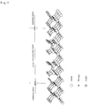
- FIG. 3 shows terminal structures of a hydrogen-terminated region and oxygen-terminated regions.
- the surface layer of a carbon crystal in each hydrogen-terminated region is terminated by hydrogen atoms, and those in the non-hydrogen-terminated regions are terminated by oxygen atoms.
- diamond single crystal was epitaxially grown by heating a diamond substrate to 850°C, introducing a mixed gas with 10% of carbon oxide gas (CO) in hydrogen gas (H 2 ) as the material gas, and applying the pressure of 35 Torr.
- CO carbon oxide gas
- H 2 hydrogen gas
- hydrocarbon such as methane, thane, butane, and ethylene.
- p-type semiconductor regions can be made by hydrogen-terminating a diamond surface.
- Methods for hydrogen-terminating the surface of diamond include, for example, a method of processing a diamond surface with hydrogen plasma (H 2 plasma), and a method of introducing hydrogen gas as the atmosphere in a reaction vessel after composing diamond by CVD, etc.
- H 2 plasma hydrogen plasma
- the surface of diamond is non-hydrogen-terminated (oxygen-terminated) by applying oxygen plasma (O 2 plasma) onto the diamond surface, exposing a diamond surface to air (oxygen) after being composed, or by irradiating argon ions onto the diamond surface, an insulating region can be made on the diamond surface.
- O 2 plasma oxygen plasma
- the present invention enables to manufacture a hydrogen-terminated diamond MISFET by forming an insulating layer on the surface of a hydrogen-terminated diamond without damaging the hydrogen-terminated surface.
- the diamond MISFET of the present invention can reduce current leakage, and has greatly improved temperature characters compared to the prior art diamond MESFET. Further, the diamond MISFET of the present invention 15 of a depression mode, but can also be changed of its mode by controlling the insulating layer thickness.
- the gate voltage decreases compared to the MES interface, which reduces the widening of the hole layer and makes it easier to change the mode to depression mode.
- the insulating layer is reduced of its thickness, the characters shown becomes closer to the characteristics shown by MESFET, and when utilizing metal of large Schottky barrier such as aluminum (Al) is used as the material for the gate electrode, the diamond MISFET can change from the depression mode to an enhancement mode.
- metal of large Schottky barrier such as aluminum (Al) is used as the material for the gate electrode
- the method for making the diamond MISFET of the present invention will be explained.
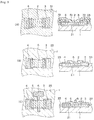
- the left figures show a plan view and the right figures show a cross-sectional view.
- the regions under the surface layer are shown by broken lines in the plan view.
- a diamond substrate is put in a plasma CVD apparatus using microwaves as its exciting source. Introduced into the plasma CVD apparatus is a mixed gas containing hydrogen (H 2 ) and a carbon-supplying gas such as methane (CH 4 ), ethane (C 2 H 6 ), butane (C 4 H 10 ), ethylene (C 2 H 4 ), carbon oxide (CO) and carbon dioxide (CO 2 ).
- the mixed gas is excited into plasma by microwaves, and diamond crystal is epitaxially grown on the surface of the diamond substrate to form a homoepitaxial diamond film 1.
- the substrate is rapidly cooled in the presence of hydrogen gas, such that hydrogen atoms bond to dangling bonds of carbon atoms in the surface layer of the diamond crystal to form the hydrogen-terminated surface 2.
- hydrogen-terminated homoepitaxial diamond substrate 1 having a surface conductive layer 21.
- Gold for example, is deposited to the surface of said hydrogen-terminated homoepitaxial diamond substrate 1 by evaporation to form a conductive layer, and then resist is applied thereto for patterning process. After that, the gold is etched to form a source electrode (ohmic contact) 3 and a drain electrode (ohmic contact) 4 (FIG. 4 (A)).
- the surface is irradiated with argon ions to provide damage to the hydrogen-terminated region 2 other than the areas being covered by the source electrode 3, the drain electrode 4 and the resist 71 in order to gain a non-hydrogen-terminated region 23.
- Under the non-hydrogen-terminated region 23 shows insulating characters with the p-type semiconductor layer being extinct (FIG. 4 (B)).
- the mask 71 is removed to further apply resist and then patterning it to form a mask 72 to the region other than the element forming region (FIG. 4 (C)).
- silicon oxide (SiO) is deposited by evaporation using resist heat evaporation device, forming a silicon oxide layer 51 shown by a chemical formula SiO x (provided 1 ⁇ X ⁇ 2) (FIG. 5(A)).
- the mask 72 is removed to lift off the silicon oxide layer 51 formed other than the element forming region, and insulating layer 5 is formed on the element forming region (FIG.5 (B)).
- a mask having an opening in the shape of the gate electrode is formed on top, depositing the gate electrode by gold and the like using evaporation method, and then the mask is removed to form the gate electrode 6, and then a plurality of MISFETs are formed on the same substrate with each element being isolated from each other (FIG. 5 (C)).
- FIG. 6 shows the voltage-current characteristic at 109°C
- FIG. 7 shows the voltage-current characteristic at 180°C.
- the MISFET used in the present embodiment is formed by irradiating argon (Ar+) ions for isolation of the plurality of MISFETs formed on the hydrogen-terminated diamond using gold (Au) as the material for the source electrode 3, the drain electrode 4 and the gate electrode 6.
- the insulating layer 5 of each MISFET is formed to have a thickness of 370 ⁇ of silicon dioxide, setting the distance between the source and the drain to be 20 ⁇ m, the width of the gate electrode to be 62 ⁇ m, and the gate length to be 13 ⁇ m.
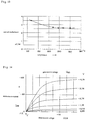
- FIG. 12 shows characteristics of the hydrogen-terminated homoepitaxial diamond MISFET operated at a temperature of 300°C.
- This MISFET uses gold (Au) as the gate metal, mounting SiO x of 680 ⁇ as the insulating layer and setting the gate length to 7 ⁇ m and the gate width to 62 ⁇ m.
- the mutual conductance as a result was 2.6mS/mm and operated at the depression mode.
- FIG. 12 puts drain-source voltage (V) on the abscissa, drain-source current (mA) on the ordinate, and takes gate-source voltages (V) as parameters.
- FIG. 13 puts operation temperature (°C) on the abscissa and mutual conductance (mS/mm) on the ordinate. Being apparent from the figure, the mutual conductance is 3.5mS/mm at 115°C, but 2.7mS/mm at 220°C, and becomes 2.6mS/mm at 245°C, 270°C and 300°C.
- platinum (Pt) could be used as the ohmic contact material. Further, platinum (Pt) could be used in lieu of gold for gate electrode. Further, aluminum (Al), lead (Pb), zinc (Zn), nickel (Ni) making high Schottky barriers, or further copper (Cu), steel (Fe), chromium (Cr) and the like could also be used.
- the present invention is related to a method of manufacturing the above-mentioned epitaxial diamond MISFET using a self-matching process.
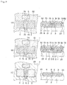
- the left figures show a plan view and the right figures show a cross-sectional view.
- a diamond substrate is put in a plasma CVD apparatus using microwaves as its exciting source. Introduced into the plasma CVD apparatus is a mixed gas containing hydrogen (H 2 ) and a carbon-supplying gas such as methane (CH 4 ), ethane (C 2 H 6 ), butane (C 4 H 10 ), ethylene (C 2 H 4 ), carbon oxide (CO) and carbon dioxide (CO 2 ).
- the mixed gas is excited into plasma by microwaves, and diamond crystal is epitaxially grown on the surface of the diamond substrate to form a homoepitaxial diamond film 1.
- the substrate is rapidly cooled in the presence of hydrogen gas, such that hydrogen atoms bond to dangling bonds of carbon atoms in the surface layer of the diamond crystal to form the hydrogen-terminated surface 2.
- hydrogen-terminated homoepitaxial diamond substrate 1 having a surface conductive layer 21.
- Gold for example, is deposited to the surface of said hydrogen-terminated homoepitaxial diamond substrate 1 by evaporation to form a conductive layer, and then the gold is etched to cofer the source region, the drain region and the channel forming region, and a metal layer 30 of gold (Au) and the like which will become a source electrode (ohmic contact) and a drain electrode (ohmic contact) is formed (FIG. 8 (A)).
- the surface is irradiated with argon ions to provide damage to the hydrogen-terminated region 2 other than the placed being covered by the source electrode 3, the drain electrode 4 and the resist 71 in order to gain a non-hydrogen-terminated region 23.
- Under the non-hydrogen-terminated region 23 shows insulating characters with the p-type semiconductor layer being extinct (FIG. 8 (B)).
- resist having resistibility to potassium iodide (KI) solution is applied and patterned to form a mask 73 having an opening 74 on the region for forming the gate electrode (FIG. 8 (C)).
- the metal layer 30 and the non-hydrogen-terminated surface 23 is exposed from the opening 74 of the mask 73.
- the KI solution is used to etch the metal layer 30 in the opening 74 of the mask 73.
- This etching is isotropic, so etching is performed not only to the lower portion of the opening 74 of the mask 73, but also to the lower area of the mask 73, forming a cavity 75.
- isolated source contact 4 and drain contact 5 are formed (FIG. 8 (D)).
- the mask 73 is used to form an insulating layer 5 by depositing an insulating material like silicon dioxide by evaporation.
- an insulating layer 5 having the same shape as the opening 74 is formed (FIG. 9 (A)).
- a gate electrode material 61 such as gold is evaporated and deposited thereto.
- a gate electrode 6 is formed on the insulating layer 5 inside the opening 74 (FIG. 9 (B)).
- a plurality of MISFETs having a hydrogen-terminated surface and forming a very thin p-type semiconductor layer under the surface and having elements isolated on the diamond layer will be formed by a self-alignment method.
- the mutual conductance in a MESFET using lead (Pb) gate electrode is 4.5mS/mm
- a MESFET gained by a self-alignment method using lead (Pb) gate electrode is 12.3mS/mm.
- the MISFET formed by the self-alignment method of the present invention is 16.4mS/mm and is very good.
- This invention uses a polycrystal diamond as the diamond and its surface is flattened by grinding, and then the surface is hydrogen-terminated to gain conductivity, and then a drain, a source and a gate electrode positioned between said drain and said source on an insulating layer is formed on this region to form a hydrogen-terminated polycrystal diamond MISFET.
- this invention forms the insulating layer of the hydrogen-terminated polycrystal diamond MISFET by a silicon oxide film shown by the chemical formula SiO x (provided 1 ⁇ X ⁇ 2).
- the MISFET was formed using a hydrogen-terminated epitaxial grown layer (homoepitaxial layer or heteroepitaxial layer).
- a hydrogen-terminated epitaxial grown layer homoepitaxial layer or heteroepitaxial layer.
- the present invention therefore, provides a hydrogen-terminated diamond MISFET suited for assembling a large scaled circuit.
- This invention uses a polycrystal diamond as the substrate having a large surface area, wherein the surface of the polycrystal diamond is grind-processed for enabling the surface to be hydrogen-terminated.
- a hydrogen-terminated polycrystal diamond region is formed by a hydrogen-termination processing (like in the first and second inventions), and forming a MISFET on said region.
- the hydrogen-terminated polycrystal diamond MISFET gained by this invention uses aluminum (Al) as the gate, the gate length being 12 ⁇ m and the gate width being 80 ⁇ m, and using silicon oxide shown by the chemical formula SiO x (provided 1 ⁇ X ⁇ 2) as the insulating layer.
- Al aluminum
- SiO x silicon oxide shown by the chemical formula SiO x (provided 1 ⁇ X ⁇ 2) as the insulating layer.
- hydrogen-termination processing could be performed by the same process as the first and second inventions on the ground and flattened polycrystal diamond surface.
- the surface of the hydrogen-terminated diamond after performing the hydrogen-termination processing could be non-hydrogen-terminated by applying an oxygen plasma processing or by irradiating argon ions as is with the first and second inventions in order to gain an insulated region.
- the surface of the polycrystal diamond could be separated to a hydrogen-terminated region and a non-hydrogen-terminated region, and FET could be formed on said terminated region to be isolated from each other.
- the source or the drain to be formed on the hydrogen processed region is formed under the ohmic contact formed of gold or platinum.
- the present inventions enables to manufacture a hydrogen-terminated diamond MISFET by forming an insulating layer on the surface of a hydrogen-terminated diamond without damaging the hydrogen-terminated surface. That is, in the above embodiment of the present invention, SiO is deposited by evaporation onto the hydrogen-terminated surface of the hydrogen-terminated diamond in order to form an insulating layer shown by the chemical formula SiO x (1 ⁇ X ⁇ 2).
- insulating material other than the above (SiO x ), such as alumina (Al 2 O 3 ), silicon oxide (Si 3 N 4 ), silicon oxide nitride (SiON), carborundum (SiC), aluminum nitride (AlN), and amorphous carbon (a-C), could also be used to form the insulating layer.
- SiO x alumina
- Si 3 N 4 silicon oxide
- SiON silicon oxide nitride
- SiC carborundum
- AlN aluminum nitride
- a-C amorphous carbon
- a MISFET having a large mutual conductance and operative in a depression mode could be gained on the surface of a hydrogen-terminated homoepitaxial diamond, and by non-hydrogen-terminating the surface of the diamond between each element, the elements could be isolated by a simple process, therefore enabling formation of a diamond semiconductor device with plurality of MISFETs being integrated.
- the mutual conductance will not change according to temperature, and the MISFET will operate stably in an environment of around 180°C.
- the present invention not only simplifies the process for making a plurality of diamond semiconductor elements on a single substrate but also enables the use of any simple configuration of FET, for example, other than a circular shape is employable, which contributes to a further miniaturization and a higher integration.
- the present invention includes a step of mounting an insulating layer (for example, SiO 2 ), so the insulating layer could be utilized for integration wiring.
- the device can be made with safety without using B 2 H 6 or other toxic gas, and can simplify equipment for fabrication without the need for accounts on such a toxic gas.
- the invention can use vapor deposition for making gate electrode, source-ohmic contacts and drain-ohmic contacts, and hence simplifies the manufacturing process.
- FETs according to the invention can be made of diamond having a large band gap, they can be used even under high temperature environment and reliably operate under intensive X rays as well.
- the process could be simplified remarkably, and increases the mutual conductance to a value as high as 3mS/mm.
- the insulating gate electrode is FET and a mask for deciding the relative position of the gate electrode to the source electrode, these electrodes could be positioned in a relatively accurate manner, and mutual conductance increases greatly.
Landscapes
- Insulated Gate Type Field-Effect Transistor (AREA)
- Thin Film Transistor (AREA)
- Recrystallisation Techniques (AREA)
Abstract
Description
Claims (50)
- A hydrogen-terminated diamond MISFET comprising a drain and a source, and a gate electrode mounted between said drain and said source on an insulating layer, mounted on a region of a diamond where a surface of said diamond is hydrogen-terminated.
- The hydrogen-terminated diamond MISFET of claim 1 wherein said diamond is either a homoepitaxial diamond or a heteroepitaxial diamond.
- The hydrogen-terminated diamond MISFET of claim 1 wherein said diamond is a polycrystal diamond with a flattened surface.
- The hydrogen-terminated diamond MISFET of claim 1 wherein said insulating layer is a silicon oxide shown by the chemical formula SiOx (provided 1≦X≦2).
- The hydrogen-terminated diamond MISFET of claim 1; whereinsaid diamond is either a homoepitaxial diamond or a heteroepitaxial diamond; andsaid insulating layer is a silicon oxide shown by the chemical formula SiOx (provided 1≦X≦2).
- The hydrogen-terminated diamond MISFET of claim 1; whereinsaid diamond is a polycrystal diamond with a flattened surface; andsaid insulating layer is a silicon oxide shown by the chemical formula SiOx (provided 1≦X≦2).
- The hydrogen-terminated diamond MISFET of claim 1; wherein said source or said drain is formed under an ohmic contact formed of gold or platinum.
- The hydrogen-terminated diamond MISFET of claim 1; whereinsaid diamond is either a homoepitaxial diamond or a heteroepitaxial diamond; andsaid source or said drain is formed under an ohmic contact formed of gold or platinum.
- The hydrogen-terminated diamond MISFET of claim 1; whereinsaid diamond is a polycrystal diamond with a flattened surface; andsaid source or said drain is formed under an ohmic contact formed of gold or platinum.
- The hydrogen-terminated diamond MISFET of claim 1; whereinsaid insulating layer is a silicon oxide shown by the chemical formula SiOx (provided 1≦X≦2); andsaid source or said drain is formed under an ohmic contact formed of gold or platinum.
- The hydrogen-terminated diamond MISFET of claim 1; whereinsaid diamond is either a homoepitaxial diamond or a heteroepitaxial diamond;said insulating layer is a silicon oxide shown by the chemical formula SiOx (provided 1≦X≦2); andsaid source or said drain is formed under an ohmic contact formed of gold or platinum.
- The hydrogen-terminated diamond MISFET of claim 1; whereinsaid diamond is a polycrystal diamond with a flattened surface;said insulating layer is a silicon oxide shown by the chemical formula SiOx (provided 1≦X≦2); andsaid source or said drain is formed under an ohmic contact formed of gold or platinum.
- A hydrogen-terminated diamond MISFET comprising a drain and a source, and a gate electrode mounted between said drain and said source on an insulating layer, mounted on a region of a diamond where a surface of said diamond is hydrogen-terminated; wherein the surface of said diamond is separated into a hydrogen-terminated region and an insulated region wherein the surface of said diamond is non-hydrogen-terminated, and FETs are formed on said hydrogen-terminated region wherein the elements are isolated.
- A hydrogen-terminated diamond MISFET comprising a drain and a source, and a gate electrode mounted between said drain and said source on an insulating layer, mounted on a region of a diamond where a surface of said diamond is hydrogen-terminated; whereinsaid diamond is either a homoepitaxial diamond or a heteroepitaxial diamond; andthe surface of said diamond is separated into a hydrogen-terminated region and an insulated region wherein the surface of said diamond is non-hydrogen-terminated, and FETs are formed on said hydrogen-terminated region wherein the elements are isolated.
- A hydrogen-terminated diamond MISFET comprising a drain and a source, and a gate electrode mounted between said drain and said source on an insulating layer, mounted on a region of a diamond where a surface of said diamond is hydrogen-terminated; whereinsaid diamond is a polycrystal diamond with a flattened surface; andthe surface of said diamond is separated into a hydrogen-terminated region and an insulated region wherein the surface of said diamond is non-hydrogen-terminated, and FETs are formed on said hydrogen-terminated region wherein the elements are isolated.
- A hydrogen-terminated diamond MISFET comprising a drain and a source, and a gate electrode mounted between said drain and said source on an insulating layer, mounted on a region of a diamond where a surface of said diamond is hydrogen-terminated; whereinsaid insulating layer is a silicon oxide shown by the chemical formula SiOx (provided 1≦X≦2); andthe surface of said diamond is separated into a hydrogen-terminated region and an insulated region wherein the surface of said diamond is non-hydrogen-terminated, and FETs are formed on said hydrogen-terminated region wherein the elements are isolated.
- A hydrogen-terminated diamond MISFET comprising a drain and a source, and a gate electrode mounted between said drain and said source on an insulating layer, mounted on a region of a diamond where a surface of said diamond is hydrogen-terminated; whereinsaid diamond is either a homoepitaxial diamond or a heteroepitaxial diamond;said insulating layer is a silicon oxide shown by the chemical formula SiOx (provided 1≦X≦2); andthe surface of said diamond is separated into a hydrogen-terminated region and an insulated region wherein the surface of said diamond is non-hydrogen-terminated, and FETs are formed on said hydrogen-terminated region wherein the elements are isolated.
- A hydrogen-terminated diamond MISFET comprising a drain and a source, and a gate electrode mounted between said drain and said source on an insulating layer, mounted on a region of a diamond where a surface of said diamond is hydrogen-terminated; whereinsaid diamond is a polycrystal diamond with a flattened surface;said insulating layer is a silicon oxide shown by the chemical formula SiOx (provided 1≦X≦2); andthe surface of said diamond is separated into a hydrogen-terminated region and an insulated region wherein the surface of said diamond is non-hydrogen-terminated, and FETs are formed on said hydrogen-terminated region wherein the elements are isolated.
- A hydrogen-terminated diamond MISFET comprising a drain and a source, and a gate electrode mounted between said drain and said source on an insulating layer, mounted on a region of a diamond where a surface of said diamond is hydrogen-terminated; whereinsaid source or said drain is formed under an ohmic contact formed of gold or platinum; andthe surface of said diamond is separated into a hydrogen-terminated region and an insulated region wherein the surface of said diamond is non-hydrogen-terminated, and FETs are formed on said hydrogen-terminated region wherein the elements are isolated.
- A hydrogen-terminated diamond MISFET comprising a drain and a source, and a gate electrode mounted between said drain and said source on an insulating layer, mounted on a region of a diamond where a surface of said diamond is hydrogen-terminated; whereinsaid diamond is either a homoepitaxial diamond or a heteroepitaxial diamond;said source or said drain is formed under an ohmic contact formed of gold or platinum; andthe surface of said diamond is separated into a hydrogen-terminated region and an insulated region wherein the surface of said diamond is non-hydrogen-terminated, and FETs are formed on said hydrogen-terminated region wherein the elements are isolated.
- A hydrogen-terminated diamond MISFET comprising a drain and a source, and a gate electrode mounted between said drain and said source on an insulating layer, mounted on a region of a diamond where a surface of said diamond is hydrogen-terminated; whereinsaid diamond is a polycrystal diamond with a flattened surface;said source or said drain is formed under an ohmic contact formed of gold or platinum; and the surface of said diamond is separated into a hydrogen-terminated region and an insulated region wherein the surface of said diamond is non-hydrogen-terminated, and FETs are formed on said hydrogen-terminated region wherein the elements are isolated.
- A hydrogen-terminated diamond MISFET comprising a drain and a source, and a gate electrode mounted between said drain and said source on an insulating layer, mounted on a region of a diamond where a surface of said diamond is hydrogen-terminated; whereinsaid insulating layer is a silicon oxide shown by the chemical formula SiOx (provided 1≦X≦2);said source or said drain is formed under an ohmic contact formed of gold or platinum; andthe surface of said diamond is separated into a hydrogen-terminated region and an insulated region wherein the surface of said diamond is non-hydrogen-terminated, and FETs are formed on said hydrogen-terminated region wherein the elements are isolated.
- A hydrogen-terminated diamond MISFET comprising a drain and a source, and a gate electrode mounted between said drain and said source on an insulating layer, mounted on a region of a diamond where a surface of said diamond is hydrogen-terminated; whereinsaid diamond is either a homoepitaxial diamond or a heteroepitaxial diamond; said insulating layer is a silicon oxide shown by the chemical formula SiOx (provided 1≦X≦ 2);said source or said drain is formed under an ohmic contact formed of gold or platinum; andthe surface of said diamond is separated into a hydrogen-terminated region and an insulated region wherein the surface of said diamond is non-hydrogen-terminated, and FETs are formed on said hydrogen-terminated region wherein the elements are isolated.
- A hydrogen-terminated diamond MISFET comprising a drain and a source, and a gate electrode mounted between said drain and said source on an insulating layer, mounted on a region of a diamond where a surface of said diamond is hydrogen-terminated; whereinsaid diamond is a polycrystal diamond with a flattened surface;said insulating layer is a silicon oxide shown by the chemical formula SiOx (provided 1≦X≦2);said source or said drain is formed under an ohmic contact formed of gold or platinum; andthe surface of said diamond is separated into a hydrogen-terminated region and an insulated region wherein the surface of said diamond is non-hydrogen-terminated, and FETs are formed on said hydrogen-terminated region wherein the elements are isolated.
- The hydrogen-terminated diamond MISFET of claims 13 through 24, wherein said non-hydrogen-terminated region comprises an oxygen-terminated diamond gained by substituting oxygen on the surface of said hydrogen-terminated diamond by oxygen plasma processing.
- The hydrogen-terminated diamond MISFET of claims 13 through 24, wherein said non-hydrogen-terminated region comprises a non-hydrogen-terminated diamond gained by irradiating argon ions onto the surface of said hydrogen-terminated diamond.
- A method for manufacturing an element-isolated hydrogen-terminated diamond MISFET, comprising the steps of:etching a metal layer formed on a diamond whose surface is hydrogen-terminated to form a source electrode and a drain electrode;creating a non-hydrogen-terminated region by non-hydrogen-terminating a hydrogen-terminated diamond region left after forming a resist on a region for forming FET electrodes;forming an insulating layer on a hydrogen-terminated region; andforming a gate electrode on said insulating layer.
- The method for manufacturing a hydrogen-terminated diamond MISFET of claim 27 wherein said diamond is either a homoepitaxial diamond or a heteroepitaxial diamond.
- The method for manufacturing a hydrogen-terminated diamond MISFET of claim 27 wherein the diamond is a polycrystal diamond with the surface being flattened.
- The method for manufacturing a hydrogen-terminated diamond MISFET of claim 27 wherein said insulating layer is a silicon oxide shown by the chemical formula SiOx (provided 1≦X≦2).
- The method for manufacturing a hydrogen-terminated diamond MISFET of claim 27; whereinsaid diamond is either a homoepitaxial diamond or a heteroepitaxial diamond; andsaid insulating layer is a silicon oxide shown by the chemical formula SiOx (provided 1≦X≦2).
- The method for manufacturing a hydrogen-terminated diamond MISFET of claim 27; whereinthe diamond is a polycrystal diamond with the surface being flattened; andsaid insulating layer is a silicon oxide shown by the chemical formula SiOx (provided 1≦X≦2).
- The method for manufacturing a hydrogen-terminated MISFET of claim 27, wherein said source electrode or said drain electrode are an ohmic-contact formed of gold or platinum.
- The method for manufacturing a hydrogen-terminated diamond MISFET of claim 27 wherein:said diamond is either a homoepitaxial diamond or a heteroepitaxial diamond; andsaid source electrode or said drain electrode are an ohmic-contact formed of gold or platinum.
- The method for manufacturing a hydrogen-terminated diamond MISFET of claim 27; whereinthe diamond is a polycrystal diamond with the surface being flattened; andsaid source electrode or said drain electrode are an ohmic-contact formed of gold or platinum.
- The method for manufacturing a hydrogen-terminated diamond MISFET of claim 27; whereinsaid insulating layer is a silicon oxide shown by the chemical formula SiOx (provided 1≦X≦2); andsaid source electrode or said drain electrode are an ohmic-contact formed of gold or platinum.
- The method for manufacturing a hydrogen-terminated diamond MISFET of claim 27; whereinsaid diamond is either a homoepitaxial diamond or a heteroepitaxial diamond;said insulating layer is a silicon oxide shown by the chemical formula SiOx (provided 1≦X≦2); andsaid source electrode or said drain electrode are an ohmic-contact formed of gold or platinum.
- The method for manufacturing a hydrogen-terminated diamond MISFET of claim 27; whereinthe diamond is a polycrystal diamond with the surface being flattened;said insulating layer is a silicon oxide shown by the chemical formula SiOx (provided 1≦X≦2); andsaid source electrode or said drain electrode are an ohmic-contact formed of gold or platinum.
- The method for manufacturing a hydrogen-terminated diamond MISFET of claim 27; wherein said non-hydrogen-terminated region is formed by either substituting oxygen on the surface of said hydrogen-terminated diamond by oxygen plasma processing, or by irradiating argon ions onto the surface of said hydrogen-terminated diamond.
- The method for manufacturing a hydrogen-terminated diamond MISFET of claim 27; whereinsaid diamond is either a homoepitaxial diamond or a heteroepitaxial diamond; andsaid non-hydrogen-terminated region is formed by either substituting oxygen on the surface of said hydrogen-terminated diamond by oxygen plasma processing, or by irradiating argon ions onto the surface of said hydrogen-terminated diamond.
- The method for manufacturing a hydrogen-terminated diamond MISFET of claim 27; whereinthe diamond is a polycrystal diamond with the surface being flattened; andsaid non-hydrogen-terminated region is formed by either substituting oxygen on the surface of said hydrogen-terminated diamond by oxygen plasma processing, or by irradiating argon ions onto the surface of said hydrogen-terminated diamond.
- The method for manufacturing a hydrogen-terminated diamond MISFET of claim 27; whereinsaid insulating layer is a silicon oxide shown by the chemical formula SiOx (provided 1≦X≦2); andsaid non-hydrogen-terminated region is formed by either substituting oxygen on the surface of said hydrogen-terminated diamond by oxygen plasma processing, or by irradiating argon ions onto the surface of said hydrogen-terminated diamond.
- The method for manufacturing a hydrogen-terminated diamond MISFET of claim 27; whereinsaid diamond is either a homoepitaxial diamond or a heteroepitaxial diamond;said insulating layer is a silicon oxide shown by the chemical formula SiOx (provided 1≦X≦2); andsaid non-hydrogen-terminated region is formed by either substituting oxygen on the surface of said hydrogen-terminated diamond by oxygen plasma processing, or by irradiating argon ions onto the surface of said hydrogen-terminated diamond.
- The method for manufacturing a hydrogen-terminated diamond MISFET of claim 27; whereinthe diamond is a polycrystal diamond with the surface being flattened;said insulating layer is a silicon oxide shown by the chemical formula SiOx (provided 1≦X≦2); andsaid non-hydrogen-terminated region is formed by either substituting oxygen on the surface of said hydrogen-terminated diamond by oxygen plasma processing, or by irradiating argon ions onto the surface of said hydrogen-terminated diamond.
- The method for manufacturing a hydrogen-terminated MISFET of claim 27; whereinsaid source electrode or said drain electrode are an ohmic-contact formed of gold or platinum; andsaid non-hydrogen-terminated region is formed by either substituting oxygen on the surface of said hydrogen-terminated diamond by oxygen plasma processing, or by irradiating argon ions onto the surface of said hydrogen-terminated diamond.
- The method for manufacturing a hydrogen-terminated diamond MISFET of claim 27 wherein:said diamond is either a homoepitaxial diamond or a heteroepitaxial diamond;said source electrode or said drain electrode are an ohmic-contact formed of gold or platinum; andsaid non-hydrogen-terminated region is formed by either substituting oxygen on the surface of said hydrogen-terminated diamond by oxygen plasma processing, or by irradiating argon ions onto the surface of said hydrogen-terminated diamond.
- The method for manufacturing a hydrogen-terminated diamond MISFET of claim 27; whereinthe diamond is a polycrystal diamond with the surface being flattened;said source electrode or said drain electrode are an ohmic-contact formed of gold or platinum; andsaid non-hydrogen-terminated region is formed by either substituting oxygen on the surface of said hydrogen-terminated diamond by oxygen plasma processing, or by irradiating argon ions onto the surface of said hydrogen-terminated diamond.
- The method for manufacturing a hydrogen-terminated diamond MISFET of claim 27; whereinsaid insulating layer is a silicon oxide shown by the chemical formula SiOx (provided 1≦X≦2);said source electrode or said drain electrode are an ohmic-contact formed of gold or platinum; andsaid non-hydrogen-terminated region is formed by either substituting oxygen on the surface of said hydrogen-terminated diamond by oxygen plasma processing, or by irradiating argon ions onto the surface of said hydrogen-terminated diamond.
- The method for manufacturing a hydrogen-terminated diamond MISFET of claim 27; whereinsaid diamond is either a homoepitaxial diamond or a heteroepitaxial diamond;said insulating layer is a silicon oxide shown by the chemical formula SiOx (provided 1≦X≦2);said source electrode or said drain electrode are an ohmic-contact formed of gold or platinum; andsaid non-hydrogen-terminated region is formed by either substituting oxygen on the surface of said hydrogen-terminated diamond by oxygen plasma processing, or by irradiating argon ions onto the surface of said hydrogen-terminated diamond.
- The method for manufacturing a hydrogen-terminated diamond MISFET of claim 27; whereinthe diamond is a polycrystal diamond with the surface being flattened;said insulating layer is a silicon oxide shown by the chemical formula SiOx (provided 1≦X≦2);said source electrode or said drain electrode are an ohmic-contact formed of gold or platinum; andsaid non-hydrogen-terminated region is formed by either substituting oxygen on the surface of said hydrogen-terminated diamond by oxygen plasma processing, or by irradiating argon ions onto the surface of said hydrogen-terminated diamond.
Applications Claiming Priority (3)
| Application Number | Priority Date | Filing Date | Title |
|---|---|---|---|
| JP232189/96 | 1996-09-02 | ||
| JP23218996 | 1996-09-02 | ||
| JP21767997A JP3364119B2 (en) | 1996-09-02 | 1997-08-12 | Hydrogen-terminated diamond MISFET and method for manufacturing the same |
Publications (2)
| Publication Number | Publication Date |
|---|---|
| EP0827208A2 true EP0827208A2 (en) | 1998-03-04 |
| EP0827208A3 EP0827208A3 (en) | 1998-04-15 |
Family
ID=26522161
Family Applications (1)
| Application Number | Title | Priority Date | Filing Date |
|---|---|---|---|
| EP97115131A Ceased EP0827208A3 (en) | 1996-09-02 | 1997-09-01 | Hydrogen-terminated diamond misfet and its manufacturing method |
Country Status (3)
| Country | Link |
|---|---|
| US (2) | US5854496A (en) |
| EP (1) | EP0827208A3 (en) |
| JP (1) | JP3364119B2 (en) |
Cited By (7)
| Publication number | Priority date | Publication date | Assignee | Title |
|---|---|---|---|---|
| WO2009005134A1 (en) | 2007-07-04 | 2009-01-08 | National Institute For Materials Science | Diamond semiconductor device |
| GB2452873B (en) * | 2006-05-10 | 2011-12-28 | Nat Inst Of Advanced Ind Scien | Method for diamond surface treatment and device using thin fi lm of diamond |
| EP2498075A3 (en) * | 2011-03-10 | 2012-10-24 | Yokogawa Electric Corporation | Semiconductor device, strain gauge, pressure sensor, and method of forming semiconductor device |
| GB2498525A (en) * | 2012-01-17 | 2013-07-24 | Diamond Microwave Devices Ltd | A diamond field effect transistor |
| US20150014707A1 (en) * | 2011-12-20 | 2015-01-15 | Universite Joseph Fourier | Method for producing a mos stack on a diamond substrate |
| US9117737B2 (en) | 2013-04-25 | 2015-08-25 | Technion Research And Development Foundation Ltd. | Molybdenum trioxide-coated hydrogen-terminated diamond surface and uses thereof |
| EP3432361A1 (en) * | 2017-07-19 | 2019-01-23 | Centre National De La Recherche Scientifique | Diamond mis transistor |
Families Citing this family (28)
| Publication number | Priority date | Publication date | Assignee | Title |
|---|---|---|---|---|
| US7589007B2 (en) * | 1999-06-02 | 2009-09-15 | Arizona Board Of Regents For And On Behalf Of Arizona State University | MESFETs integrated with MOSFETs on common substrate and methods of forming the same |
| SE515494C2 (en) * | 1999-12-28 | 2001-08-13 | Abb Ab | High voltage semiconductor device and method for manufacturing a passivation layer on a high voltage semiconductor device |
| FR2868209B1 (en) * | 2004-03-25 | 2006-06-16 | Commissariat Energie Atomique | FIELD-FIELD FIELD EFFECT TRANSISTOR DIAMOND CARBON |
| JP2006010359A (en) * | 2004-06-22 | 2006-01-12 | Keio Gijuku | Termination method of diamond electrode |
| JP4408787B2 (en) * | 2004-10-19 | 2010-02-03 | 株式会社神戸製鋼所 | Insulating film, manufacturing method thereof, and electronic device provided with insulating film |
| JP4817813B2 (en) * | 2005-11-15 | 2011-11-16 | 株式会社神戸製鋼所 | Diamond semiconductor device and manufacturing method thereof |
| DE112007001892T5 (en) * | 2006-08-11 | 2009-06-10 | Akhan Technologies, Inc., Schaumburg | Nanocrystalline diamond P-channel field effect transistor |
| JP5095562B2 (en) * | 2008-09-05 | 2012-12-12 | 日本電信電話株式会社 | Diamond field effect transistor and manufacturing method thereof |
| JP5483168B2 (en) * | 2009-07-24 | 2014-05-07 | 日本電信電話株式会社 | Diamond thin film and diamond field effect transistor |
| DE102010053214A1 (en) * | 2010-12-03 | 2012-06-06 | Evonik Degussa Gmbh | Process for the hydrogen passivation of semiconductor layers |
| JP5759398B2 (en) * | 2012-02-21 | 2015-08-05 | 日本電信電話株式会社 | Diamond field effect transistor and method for producing the same |
| GB2504613A (en) * | 2012-07-17 | 2014-02-05 | Element Six Technologies Us Corp | Integrated diamond p-channel FETs and GaN n-channel FETs |
| JP6218062B2 (en) * | 2012-08-24 | 2017-10-25 | 学校法人早稲田大学 | Power element, power control device, and method of manufacturing power element |
| CN102903756A (en) * | 2012-09-07 | 2013-01-30 | 中国电子科技集团公司第五十五研究所 | Field effect transistor with diamond metal-insulator-semiconductor structure and preparation method thereof |
| CN103280395B (en) * | 2013-05-17 | 2015-07-08 | 中国电子科技集团公司第十三研究所 | Thermal annealing method for manufacturing hydrogen end group conducting channel on diamond face |
| JP6712735B2 (en) * | 2015-02-25 | 2020-06-24 | 学校法人早稲田大学 | Power device |
| JP6534036B2 (en) * | 2015-07-09 | 2019-06-26 | 国立大学法人金沢大学 | Field-effect transistor using hydrogen-terminated diamond |
| JP2017045897A (en) * | 2015-08-27 | 2017-03-02 | 学校法人早稲田大学 | Diamond field effect transistor and manufacturing method therefor |
| JP6713167B2 (en) * | 2016-06-06 | 2020-06-24 | 国立研究開発法人物質・材料研究機構 | Triple gate H-diamond MISFET and manufacturing method thereof |
| JP2018032662A (en) * | 2016-08-22 | 2018-03-01 | 国立大学法人名古屋大学 | Diamond contact structure and electronic device using the same |
| JP6783463B2 (en) * | 2016-11-11 | 2020-11-11 | 国立研究開発法人物質・材料研究機構 | Diamond semiconductor device, logic device using it, and manufacturing method of diamond semiconductor device |
| CN107393815B (en) * | 2017-09-05 | 2019-11-19 | 中国电子科技集团公司第十三研究所 | Preparation method of diamond-based field effect transistor and field effect transistor |
| JP7491547B2 (en) | 2020-03-10 | 2024-05-28 | 学校法人早稲田大学 | Diamond field effect transistor and method of manufacturing same |
| JP7804982B2 (en) * | 2020-12-29 | 2026-01-23 | 大熊ダイヤモンドデバイス株式会社 | field-effect transistor |
| CN113871464A (en) * | 2021-08-27 | 2021-12-31 | 中国电子科技集团公司第十三研究所 | Silicon terminated diamond field effect transistor and method of making the same |
| JP2025000357A (en) * | 2023-06-19 | 2025-01-07 | 大熊ダイヤモンドデバイス株式会社 | Diamond semiconductor element, electrical machinery and equipment, and method for manufacturing diamond semiconductor element |
| WO2025196945A1 (en) * | 2024-03-19 | 2025-09-25 | Ntt株式会社 | Spin valve, method for manufacturing same, and spin device |
| CN119133182B (en) * | 2024-09-04 | 2025-12-02 | 西安交通大学 | A diamond-based CMOS inverter and its fabrication method |
Family Cites Families (8)
| Publication number | Priority date | Publication date | Assignee | Title |
|---|---|---|---|---|
| US5216264A (en) * | 1989-06-07 | 1993-06-01 | Sharp Kabushiki Kaisha | Silicon carbide MOS type field-effect transistor with at least one of the source and drain regions is formed by the use of a schottky contact |
| JP2813023B2 (en) * | 1990-03-13 | 1998-10-22 | 株式会社神戸製鋼所 | MIS type diamond field effect transistor |
| US5500393A (en) * | 1990-05-21 | 1996-03-19 | Sumitomo Electric Industries, Ltd. | Method for fabricating a schottky junction |
| US5238866A (en) * | 1991-09-11 | 1993-08-24 | GmbH & Co. Ingenieurburo Berlin Biotronik Mess- und Therapiegerate | Plasma enhanced chemical vapor deposition process for producing an amorphous semiconductive surface coating |
| US5459107A (en) * | 1992-06-05 | 1995-10-17 | Cree Research, Inc. | Method of obtaining high quality silicon dioxide passivation on silicon carbide and resulting passivated structures |
| US5322802A (en) * | 1993-01-25 | 1994-06-21 | North Carolina State University At Raleigh | Method of fabricating silicon carbide field effect transistor |
| JP3308755B2 (en) * | 1994-09-16 | 2002-07-29 | 東京瓦斯株式会社 | Method for manufacturing hydrogen-terminated diamond semiconductor device with element isolation |
| US5455432A (en) * | 1994-10-11 | 1995-10-03 | Kobe Steel Usa | Diamond semiconductor device with carbide interlayer |
-
1997
- 1997-08-12 JP JP21767997A patent/JP3364119B2/en not_active Expired - Fee Related
- 1997-08-29 US US08/919,792 patent/US5854496A/en not_active Expired - Fee Related
- 1997-09-01 EP EP97115131A patent/EP0827208A3/en not_active Ceased
-
1998
- 1998-09-22 US US09/158,066 patent/US6025211A/en not_active Expired - Fee Related
Cited By (11)
| Publication number | Priority date | Publication date | Assignee | Title |
|---|---|---|---|---|
| GB2452873B (en) * | 2006-05-10 | 2011-12-28 | Nat Inst Of Advanced Ind Scien | Method for diamond surface treatment and device using thin fi lm of diamond |
| WO2009005134A1 (en) | 2007-07-04 | 2009-01-08 | National Institute For Materials Science | Diamond semiconductor device |
| EP2169709A4 (en) * | 2007-07-04 | 2011-06-22 | Nat Inst For Materials Science | DIAMOND SEMICONDUCTOR DEVICE |
| EP2498075A3 (en) * | 2011-03-10 | 2012-10-24 | Yokogawa Electric Corporation | Semiconductor device, strain gauge, pressure sensor, and method of forming semiconductor device |
| US20150014707A1 (en) * | 2011-12-20 | 2015-01-15 | Universite Joseph Fourier | Method for producing a mos stack on a diamond substrate |
| US9337034B2 (en) * | 2011-12-20 | 2016-05-10 | Centre National De La Recherche Scientifique | Method for producing a MOS stack on a diamond substrate |
| GB2498525A (en) * | 2012-01-17 | 2013-07-24 | Diamond Microwave Devices Ltd | A diamond field effect transistor |
| US9117737B2 (en) | 2013-04-25 | 2015-08-25 | Technion Research And Development Foundation Ltd. | Molybdenum trioxide-coated hydrogen-terminated diamond surface and uses thereof |
| EP3432361A1 (en) * | 2017-07-19 | 2019-01-23 | Centre National De La Recherche Scientifique | Diamond mis transistor |
| WO2019016268A1 (en) * | 2017-07-19 | 2019-01-24 | Centre National De La Recherche Scientifique | Diamond mis transistor |
| US11569381B2 (en) | 2017-07-19 | 2023-01-31 | Centre National De La Recherche Scientifique | Diamond MIS transistor |
Also Published As
| Publication number | Publication date |
|---|---|
| JPH10125932A (en) | 1998-05-15 |
| US5854496A (en) | 1998-12-29 |
| EP0827208A3 (en) | 1998-04-15 |
| JP3364119B2 (en) | 2003-01-08 |
| US6025211A (en) | 2000-02-15 |
Similar Documents
| Publication | Publication Date | Title |
|---|---|---|
| US5854496A (en) | Hydrogen-terminated diamond misfet and its manufacturing method | |
| US5786604A (en) | Element-isolated hydrogen-terminated diamond semiconductor device and its manufacturing method | |
| US5173761A (en) | Semiconducting polycrystalline diamond electronic devices employing an insulating diamond layer | |
| US7507999B2 (en) | Semiconductor device and method for manufacturing same | |
| US5170231A (en) | Silicon carbide field-effect transistor with improved breakdown voltage and low leakage current | |
| KR920002090B1 (en) | Method of manufacturing field effect transistor | |
| EP0588260B1 (en) | Diamond semiconductor device | |
| KR970004457B1 (en) | Semiconductor device and manufacturing method thereof | |
| US6091122A (en) | Fabrication of mid-cap metal gates compatible with ultra-thin dielectrics | |
| US5135885A (en) | Method of manufacturing silicon carbide fets | |
| US5523588A (en) | Diamond film field effect transistor with self aligned source and drain regions | |
| US5216264A (en) | Silicon carbide MOS type field-effect transistor with at least one of the source and drain regions is formed by the use of a schottky contact | |
| JP7054853B2 (en) | Silicon carbide semiconductor device and its manufacturing method | |
| US6639279B1 (en) | Semiconductor transistor having interface layer between semiconductor and insulating layers | |
| JP3714803B2 (en) | Method for manufacturing diamond field effect transistor | |
| JP3432367B2 (en) | Hydrogen terminated diamond depletion type MESFET and method of manufacturing the depletion type MESFET | |
| JP3269510B2 (en) | Semiconductor element | |
| US6262462B1 (en) | Enhanced dielectric constant gate insulator | |
| US5539248A (en) | Semiconductor device with improved insulating/passivating layer of indium gallium fluoride (InGaF) | |
| KR20030075749A (en) | HFET device and semiconductor device having iridium-containing gate electrode and methods for manufacturing the same | |
| US20250336744A1 (en) | Semiconductor devices with oxidized layer segments in device regions | |
| US12520552B2 (en) | Method of manufacturing a semiconductor device and semiconductor device | |
| JP3383737B2 (en) | Manufacturing method of hydrogen-terminated diamond FET by self-alignment method | |
| JP2798045B2 (en) | Method of controlling threshold voltage of field effect transistor | |
| US20090026497A1 (en) | Method for Producing Semiconductor Device |
Legal Events
| Date | Code | Title | Description |
|---|---|---|---|
| PUAI | Public reference made under article 153(3) epc to a published international application that has entered the european phase |
Free format text: ORIGINAL CODE: 0009012 |
|
| PUAL | Search report despatched |
Free format text: ORIGINAL CODE: 0009013 |
|
| AK | Designated contracting states |
Kind code of ref document: A2 Designated state(s): DE FR GB |
|
| AK | Designated contracting states |
Kind code of ref document: A3 Designated state(s): AT BE CH DE DK ES FI FR GB GR IE IT LI LU MC NL PT SE |
|
| 17P | Request for examination filed |
Effective date: 19980731 |
|
| AKX | Designation fees paid |
Free format text: DE FR GB |
|
| RBV | Designated contracting states (corrected) |
Designated state(s): DE FR GB |
|
| 17Q | First examination report despatched |
Effective date: 19981229 |
|
| STAA | Information on the status of an ep patent application or granted ep patent |
Free format text: STATUS: THE APPLICATION HAS BEEN REFUSED |
|
| 18R | Application refused |
Effective date: 19991113 |