EP0821348A2 - Tête magnétique découplée - Google Patents
Tête magnétique découplée Download PDFInfo
- Publication number
- EP0821348A2 EP0821348A2 EP97111209A EP97111209A EP0821348A2 EP 0821348 A2 EP0821348 A2 EP 0821348A2 EP 97111209 A EP97111209 A EP 97111209A EP 97111209 A EP97111209 A EP 97111209A EP 0821348 A2 EP0821348 A2 EP 0821348A2
- Authority
- EP
- European Patent Office
- Prior art keywords
- magnetic
- shields
- poles
- magnetic head
- shield
- Prior art date
- Legal status (The legal status is an assumption and is not a legal conclusion. Google has not performed a legal analysis and makes no representation as to the accuracy of the status listed.)
- Withdrawn
Links
Images


Classifications
-
- G—PHYSICS
- G11—INFORMATION STORAGE
- G11B—INFORMATION STORAGE BASED ON RELATIVE MOVEMENT BETWEEN RECORD CARRIER AND TRANSDUCER
- G11B5/00—Recording by magnetisation or demagnetisation of a record carrier; Reproducing by magnetic means; Record carriers therefor
- G11B5/127—Structure or manufacture of heads, e.g. inductive
- G11B5/33—Structure or manufacture of flux-sensitive heads, i.e. for reproduction only; Combination of such heads with means for recording or erasing only
- G11B5/39—Structure or manufacture of flux-sensitive heads, i.e. for reproduction only; Combination of such heads with means for recording or erasing only using magneto-resistive devices or effects
- G11B5/3903—Structure or manufacture of flux-sensitive heads, i.e. for reproduction only; Combination of such heads with means for recording or erasing only using magneto-resistive devices or effects using magnetic thin film layers or their effects, the films being part of integrated structures
- G11B5/3967—Composite structural arrangements of transducers, e.g. inductive write and magnetoresistive read
-
- G—PHYSICS
- G11—INFORMATION STORAGE
- G11B—INFORMATION STORAGE BASED ON RELATIVE MOVEMENT BETWEEN RECORD CARRIER AND TRANSDUCER
- G11B5/00—Recording by magnetisation or demagnetisation of a record carrier; Reproducing by magnetic means; Record carriers therefor
- G11B5/127—Structure or manufacture of heads, e.g. inductive
- G11B5/31—Structure or manufacture of heads, e.g. inductive using thin films
- G11B5/3103—Structure or manufacture of integrated heads or heads mechanically assembled and electrically connected to a support or housing
- G11B5/3106—Structure or manufacture of integrated heads or heads mechanically assembled and electrically connected to a support or housing where the integrated or assembled structure comprises means for conditioning against physical detrimental influence, e.g. wear, contamination
-
- G—PHYSICS
- G11—INFORMATION STORAGE
- G11B—INFORMATION STORAGE BASED ON RELATIVE MOVEMENT BETWEEN RECORD CARRIER AND TRANSDUCER
- G11B5/00—Recording by magnetisation or demagnetisation of a record carrier; Reproducing by magnetic means; Record carriers therefor
- G11B5/48—Disposition or mounting of heads or head supports relative to record carriers ; arrangements of heads, e.g. for scanning the record carrier to increase the relative speed
- G11B5/488—Disposition of heads
- G11B5/4886—Disposition of heads relative to rotating disc
-
- G—PHYSICS
- G11—INFORMATION STORAGE
- G11B—INFORMATION STORAGE BASED ON RELATIVE MOVEMENT BETWEEN RECORD CARRIER AND TRANSDUCER
- G11B5/00—Recording by magnetisation or demagnetisation of a record carrier; Reproducing by magnetic means; Record carriers therefor
- G11B5/48—Disposition or mounting of heads or head supports relative to record carriers ; arrangements of heads, e.g. for scanning the record carrier to increase the relative speed
- G11B5/488—Disposition of heads
- G11B5/4893—Disposition of heads relative to moving tape
-
- G—PHYSICS
- G11—INFORMATION STORAGE
- G11B—INFORMATION STORAGE BASED ON RELATIVE MOVEMENT BETWEEN RECORD CARRIER AND TRANSDUCER
- G11B5/00—Recording by magnetisation or demagnetisation of a record carrier; Reproducing by magnetic means; Record carriers therefor
- G11B5/127—Structure or manufacture of heads, e.g. inductive
- G11B5/31—Structure or manufacture of heads, e.g. inductive using thin films
- G11B5/3109—Details
- G11B5/313—Disposition of layers
-
- G—PHYSICS
- G11—INFORMATION STORAGE
- G11B—INFORMATION STORAGE BASED ON RELATIVE MOVEMENT BETWEEN RECORD CARRIER AND TRANSDUCER
- G11B5/00—Recording by magnetisation or demagnetisation of a record carrier; Reproducing by magnetic means; Record carriers therefor
- G11B5/127—Structure or manufacture of heads, e.g. inductive
- G11B5/31—Structure or manufacture of heads, e.g. inductive using thin films
- G11B5/3163—Fabrication methods or processes specially adapted for a particular head structure, e.g. using base layers for electroplating, using functional layers for masking, using energy or particle beams for shaping the structure or modifying the properties of the basic layers
Definitions
- This invention relates to magnetic heads and in particular to magnetic heads having magnetic read elements disposed coplanar with magnetic write elements.
- Magnetic data storage systems typically include a magnetic recording medium, such as a magnetic disk or tape, and magnetic heads or transducers that coact with the medium to write and read data.
- a magnetic recording medium such as a magnetic disk or tape
- magnetic heads or transducers that coact with the medium to write and read data.
- disk drives incorporating magnetic disks are widely used for storage of data.
- Magnetic transducers or heads interact with the magnetic recording medium to write and read data.
- inductive heads or transducers were used for both writing and reading data.
- magnetoresistive (MR) sensors or MR read transducers are used for reading data recorded by inductive write heads.
- An MR transducer can read information on a magnetic recording medium with much narrower track widths and operates with an improved signal-to-noise ratio.
- the output signal generated during the read process is independent of the traveling speed of the recording medium. Consequently, a higher recording density on the magnetic recording medium is made possible.
- a magnetic head with a merged design typically includes an MR sensor sandwiched between a magnetic shield layer and a first pole layer which also serves as a second shield. The MR sensor is separated from the shield and pole layer by insulating material. A second pole layer is deposited above the first pole layer with an inductive coil surrounded by insulating material between the pole layers. The two magnetic pole layers come into direct contact with each other at a back region at one end and are separated from each other by a narrow insulating layer at an opposite end to provide a transducing gap which serves as a write gap.
- the inductive coil During the write mode, electrical current representing data is passed through the inductive coil.
- the current-carrying coil induces magnetic flux in the magnetic poles.
- the induced magnetic flux flows through the poles along the continuous magnetic path formeed by the magnetic poles, and reaches the narrow gap so that a closely adjacent moving magnetic medium registers and stores data signals representative of the magnetic flux.
- the magnetic shield and the first pole act as magnetic shields so that only flux from the closest bit transition in the magnetic storage medium can be sensed by the MR sensor.
- the magnetic medium has recorded transitions that provide changes in magnetic flux which correspondingly varies the resistivity of the MR element of the read sensor.
- a direct electric current passing through the MR element generates a varying voltage which represents the data stored in the magnetic medium.
- the first pole serves dual functions as a shield for the MR sensor as well as a pole for the inductive transducer.
- the need for an extra shield layer and the associated necessary processing steps during manufacture are eliminated.
- each transducer can be designed independently.
- the MR element can be built at a miniaturized scale, thereby allowing the magnetic head to read information on a recording medium with much narrower data track widths.
- the inductive write transducer can be fabricated with less turns which reduces inductance of the coil.
- a magnetic head comprises many layers in which the overlying layers are less orderly in surface regularity than the underlying layers. That is, the overlying layers in a multilayer structure encounter more topographical unevenness than the lower layers. As a consequence, the probability of experiencing processing defects in the overlying layers are higher. The processing defects directly affect manufacturing yield and performance reliability of the magnetic head.
- the read transducer In processing a merged head, the read transducer is always fabricated prior to the write transducer.
- the rationale behind this fabrication sequence is because the material layers constituting the read transducer, being thinner and more delicate, need to be deposited on the lower layers closer to the substrate for a flat underlying support. Accordingly, the thin layers of the read transducer experience the subsequent high temperature photoresist curing process required for making the insulations between inductive coil turns. Excessive high heat may damage the thin and delicate layers of the read transducer. This problem worsens when thinner spin-valve or multilayered GMR sensors are used. As a consequence, the overall production yield may further be compromised.
- Another approach is to form extensive and flat underlying layers as a base for the subsequently deposited layers.
- the drawback with this approach is that the magnetic shield layer is made of ferromagnetic material.
- the mutual inductance caused by the extensive magnetic shield layer impinging upon the inductive coil is significant.
- An inductive coil with high inductance is sluggish in response to write current and cannot function at high frequency ranges.
- the coupling arrangement of the read and write transducers in a conventional merged head also restrains the performance of the head during normal operations.
- the first pole assumes a dual role as a shield for the read sensor and as a pole for the inductive transducer.
- the read transducer is prone to pick up signal noise from two areas.
- stray magnetic flux from the first pole induced by the current during the write mode can cause magnetic domain instability in the read transducer itself, consequently causing signal noise during the read mode.
- the inductive transducer has relatively high current which in turn generates substantial Joule heat surrounding the coil.
- the write current When the write current is stopped, mismatches in thermal contraction between the adjacent dielectric material and the second pole create magnetic domain instabilities in the first pole.
- the magnetic domain instabilities progress into splitting or merging of the magnetic domains, which consequently manifest themselves as Barkhausen noise or popcorn noise impinging upon the read transducer during data reading.
- the extensive magnetic shield contributes significant mutual inductance to the inductive coil, and consequently renders the coil sluggish in response.
- An object of the invention is to provide a magnetic head having a reduced number of layers and a simplified design, thereby facilitating manufacture and realizing improved production yield.
- Another object of the invention is to provide a magnetic head having read and write transducers which interfere minimally with each other during normal operations and accordingly maximize head performance.
- a magnetic head is fabricated with at least one read transducer disposed in juxtaposition with a write transducer on a substrate.
- the write transducer includes an inductive coil sandwiched between first and second magnetic poles.
- the read transducer comprises an MR read sensor interposed between first and second magnetic shields.
- the first and second magnetic shields are dielectrically separated from and substantially coplanar with the first and second magnetic poles, respectively.
- the number of material layers in the magnetic head is reduced as the first pole and the first shield can be fabricated simultaneously.
- the second pole and second shield can be fabricated simultaneously. With a reduced number of layers, the magnetic head of the invention poses less of a step coverage problem in processing.
- the read and write transducers interfere less with each other during normal operations.
- a magnetic head 12 is formed on a substrate 4, preferably made of a ceramic material that is nonmagnetic and nonconducting.
- the magnetic head 2 includes a pair of read transducers 6 and 8, and a write transducer 10 disposed in juxtaposition and adjacent to an air bearing surface 12. Electrical leads are connected to the transducers 6, 8 and 10. Specifically, leads 14 and 16 are connected to the read transducer 6; leads 18 and 20 are connected to the write transducer 10; and leads 22 and 24 are connected to the read transducer 8.
- Fig. 2 shows the positional relationships of the various layers of the magnetic head 2.
- a first pole 28 is formed over the substrate 4 and a second pole 30 is disposed over the first pole 28.
- the first pole 28 and the second pole 30 are separated at one end by an insulating gap layer 32, and are in contact at another end called a back gap region 34 (Fig. 1).
- the poles 30 and 34 form a continuous magnetic path.
- a data write means 36 Disposed between the first and second poles 28 and 30 is a data write means 36 which includes an inductive coil 38.
- the read transducers 6 and 8 are positioned on each side of the write transducer 10.
- a first shield 40 is disposed on top of the substrate 4.
- a second shield 42 is formed above the first shield 40 is.
- the rust and second shields 40 and 42 are separated by an insulating read gap layer 45.
- the insulating read gap layer 45 and the write gap layer 32 are separately deposited and may have different thicknesses. For the sake of clarity, the lines partitioning the two insulating layers 32 and 45 are not shown in the drawings.
- Data readout means 44 is positioned between the First shield 40 and the second shield 42.
- data readout means 44 preferably comprises at least one MR sensor in the form of either an anisotropic magnetoresistive (AMR) sensor, or a giant magnetoresistive (GMR) sensor.
- AMR anisotropic magnetoresistive
- GMR giant magnetoresistive
- the data readout means 44 comprises two MR elements sandwiched between and dielectrically separated from a third shield 48 and a fourth shield 50 through an insulating read gap layer 52.
- the first pole 28, the first shield 40 and the third shield 48 are substantially coplanar.
- the second pole 30, the second shield 42 and the fourth shield 50 are substantially coplanar.
- the read transducers 6 and 8 are free from any interference which may be caused by the write transducer 10.
- the coil 38 (Fig.1) carries a substantial amount of current during data writing. The data write current consequently generates considerable Joule heat surrounding the coil. Upon stopping the write current, mismatches in thermal contraction between the adjacent dielectric material and the poles 28 and 30 create magnetic domain instabilities in the poles 28 and 30.
- the magnetic head 2 shown in Figs. 1 and 2 should be contrasted with a prior art merged head 54 illustrated in Fig. 3.
- the merged head 54 includes a first pole 59 dielectrically separated from a second pole 55.
- An inductive coil (not shown) is sandwiched between the first pole 59 and the second pole 55.
- the first pole 59 performs the dual functions as a pole for the coil (not shown) and as a shield for the read sensor 56.
- the head 54 is in operation and is switching from the write mode to the read mode.
- the second shield 59 undesirably captures the domain instabilities to the fullest extent.
- the read sensor 56 correspondingly senses considerable signal noise, commonly called Barkhausen noise, in addition to the sensed signal.
- the magnetic head 2 of the invention also poses less complication in fabrication in contrast to the prior art merged head 54, shown in Fig. 3.
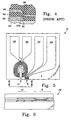
- Fig. 4 illustrates the problem of step coverage commonly encountered in the prior art when producing thin film products.
- a metallic layer 58 is formed over a substrate layer 60 having a step 62.
- an insulating layer 64 is deposited on top of the metallic layer 58 and the substrate 60.
- Another metallic layer 66 is formed on the insulating layer 64.
- the overlying layers 64 and 66 have a tendency to evenly distribute the deposited material along the direction of deposition. As a consequence, areas devoid of deposited material above the step edge 62A, such as areas 68, may result. If the areas with material deficiency occurs in the metallic layer 66, there will be an open circuit. If the area devoid of material happens in the insulating layer 64, there will be an electrical short bridging the overlying and underlying layers 66 and 58. If the metallic layer 66 is one of the windings of an inductive transducer, it will be a malfunctioning transducer. The higher the layer number, the more exacerbated the problem of step coverage.
- any electrical open or short in any winding will negatively affect the manufacturing yield and performance reliability. It is for this reason that in a multilayer structure, the underlying layers have to wide and extensive in area in order to provide a level foundation for the overlying layers.
- the magnetic shield 57 has to be wide and extensive. In conjunction with an extensive area, the magnetic head 57 contributes substantial mutual inductance to the coil and deleteriously affects the performance of the write function of the merged head 54.
- the transducer 10 of the magnetic head 2 of the invention shown in Figs. 1 and 2 does not have such restraint. Since the coil 38 is located at a layer closer to the substrate 4, instead of at a higher layer as in the head 54 shown in Fig. 3, step coverage is less of a problem. Consequently, there is more freedom in the dimensional design of the first pole 28 (Fig. 2). With this arrangement, the first pole 28 affects performance less as a result of mutual inductance to the coil 38.
- the write transducer 36 can be properly responsive to write current and is capable of operating at high frequency bandwidths.
- the magnetic head 2 For fabricating the magnetic head 2, conventional thin film processing techniques can be employed. For the sake of clarity and conciseness, the well-known processing techniques are not elaborated herein. It should be noted that the write coil 38 and insulations can be formed prior to the MR read sensors 46. Accordingly, the MR read sensors 46 do not experience the high heat curing process used for the photoresist which surrounds the data write coil 38. The aforementioned sequence cannot be applied to the prior art merged head 54 shown in Fig. 3. The "write-head-first" fabrication sequence of this invention also allows for several different degrees of freedom, such as trenched write heads and track width definition by the leading pole for very narrow write heads.
- the embodiment described above is built with two read transducers 6 and 8.
- the main purpose for this arrangement is to allow the magnetic head 2, and its conjugate, to interact with a doubled-sided magnetic disk.
- the transducer 6 for the magnetic head 2 is designated as the read transducer and reads data on a recorded track on one side of a magnetic disk.
- a similar magnetic head 2, mounted on the other side of the magnetic disk, may designate the transducer 8 as the read transducer to read a corresponding data track with the same track number on the other side of the disk.
- Another reason for having the two transducers 6 and 8 implemented in the magnetic head 2 is improve production yield. As the MR sensors 46 are delicately deposited with various ultra- fine layers, defect occurences, if any, are more concentrated in these areas of the head 2 than any other areas. Accordingly, it is preferable to match the read transducers 6 and 8 for each coil 38. In the event that one transducer does not pass the final test, the other transducer can be utilized.
- a simplified example may serve as an illustration. Suppose in a production lot in which the yield is 50% and the defects occur predominantly on the read transducers. If only one read transducer is paired up with one write transducer on each die of a production wafer, 50% of the dies will have to be discarded.
- the final yield of accepted dies falls within the range between 50% to 100%.
- the actual yield would depend on the random nature of the defects. The more evenly distributed the defects, the higher will be the final yield.
- the magnetic head 70 shown in Fig. 5 may be used in another embodiment.
- the magnetic head 70 is suitable for interacting with one side of the magnetic disks or tapes.
- the write transducer 10 is connected to the electrical leads 18 and 20.
- the read transducer 8 is connected to the electrical leads 22 and 24.
- Fig. 6 is an elevational view taken from the line 6-6 of Fig. 5.
- the structural and operational details of this embodiment is substantially similar to the previous embodiment. For reason of conciseness, they are not further repeated.
- Fig. 7 shows an alternative version of the invention wherein a magnetic head 72 has a first pole 74 coplanar with a second shield 80 and a fourth shield 84. There is a first shield 78 disposed coplanar with a third shield 82.
- Fig. 8 shows yet another variation of the invention of a magnetic head 86 having a second pole 88 disposed coplanar with a first shield 92 and a third shield 96. There is a second shield 94 disposed coplanar with a fourth shield 98.
- the read transducers need not be disposed separately with one read transducer placed on one side of the write transducer. Both read transducers can be positioned on only one side of the write transducer.
Applications Claiming Priority (2)
| Application Number | Priority Date | Filing Date | Title |
|---|---|---|---|
| US69031696A | 1996-07-25 | 1996-07-25 | |
| US690316 | 1996-07-25 |
Publications (2)
| Publication Number | Publication Date |
|---|---|
| EP0821348A2 true EP0821348A2 (fr) | 1998-01-28 |
| EP0821348A3 EP0821348A3 (fr) | 1998-03-04 |
Family
ID=24771998
Family Applications (1)
| Application Number | Title | Priority Date | Filing Date |
|---|---|---|---|
| EP97111209A Withdrawn EP0821348A3 (fr) | 1996-07-25 | 1997-07-03 | Tête magnétique découplée |
Country Status (2)
| Country | Link |
|---|---|
| EP (1) | EP0821348A3 (fr) |
| JP (1) | JPH1069615A (fr) |
Cited By (7)
| Publication number | Priority date | Publication date | Assignee | Title |
|---|---|---|---|---|
| US7343667B2 (en) | 2004-09-30 | 2008-03-18 | Hitachi Global Storage Technologies Netherlands B.V. | Methods of making a side-by-side read/write head with a self-aligned trailing shield structure |
| CN100383857C (zh) * | 2004-11-15 | 2008-04-23 | 三星电子株式会社 | 磁记录头 |
| US7692893B2 (en) | 2004-06-30 | 2010-04-06 | Hitachi Global Storage Technologies Netherlands, B.V. | Side-by-side magnetic head configuration with flared pole tip layer and read sensor sharing same plane |
| US20140334042A1 (en) * | 2013-03-08 | 2014-11-13 | Seagate Technology Llc | Reader with decoupled magnetic seed layer |
| US9299369B1 (en) | 2014-10-29 | 2016-03-29 | International Business Machines Corporation | Multichannel data storage apparatus having abrasion resistant barrier |
| US9418683B2 (en) | 2014-10-29 | 2016-08-16 | International Business Machines Corporation | Mass production of multichannel current perpendicular to plane head modules via preferred milling |
| US9449622B2 (en) | 2014-10-29 | 2016-09-20 | International Business Machines Corporation | Differing magnetic read sensors on a magnetic head |
Citations (7)
| Publication number | Priority date | Publication date | Assignee | Title |
|---|---|---|---|---|
| JPS6212913A (ja) * | 1985-07-10 | 1987-01-21 | Hitachi Ltd | マルチトラツク磁気抵抗効果型磁気ヘツド |
| JPH03207007A (ja) * | 1990-01-10 | 1991-09-10 | Matsushita Electric Ind Co Ltd | 薄膜磁気ヘッド |
| EP0492848A2 (fr) * | 1990-12-26 | 1992-07-01 | International Business Machines Corporation | Tête transductrice et procédé de fabrication |
| US5212611A (en) * | 1991-07-16 | 1993-05-18 | Storage Technology Corporation | Integral read/write recording head with dual gap dimension |
| WO1994005007A2 (fr) * | 1992-08-21 | 1994-03-03 | Minnesota Mining And Manufacturing Company | Ensemble tete de lecture et d'ecriture magnetoresistive bidirectionnelle a couche mince |
| EP0631275A2 (fr) * | 1993-06-28 | 1994-12-28 | Tandberg Data A/S | Assemblage de têtes avec faible distance entre les têtes de lecture/écriture |
| JPH07296343A (ja) * | 1994-04-27 | 1995-11-10 | Sony Corp | 磁気抵抗効果型磁気ヘッドの製造方法 |
-
1997
- 1997-07-03 EP EP97111209A patent/EP0821348A3/fr not_active Withdrawn
- 1997-07-25 JP JP21391597A patent/JPH1069615A/ja active Pending
Patent Citations (7)
| Publication number | Priority date | Publication date | Assignee | Title |
|---|---|---|---|---|
| JPS6212913A (ja) * | 1985-07-10 | 1987-01-21 | Hitachi Ltd | マルチトラツク磁気抵抗効果型磁気ヘツド |
| JPH03207007A (ja) * | 1990-01-10 | 1991-09-10 | Matsushita Electric Ind Co Ltd | 薄膜磁気ヘッド |
| EP0492848A2 (fr) * | 1990-12-26 | 1992-07-01 | International Business Machines Corporation | Tête transductrice et procédé de fabrication |
| US5212611A (en) * | 1991-07-16 | 1993-05-18 | Storage Technology Corporation | Integral read/write recording head with dual gap dimension |
| WO1994005007A2 (fr) * | 1992-08-21 | 1994-03-03 | Minnesota Mining And Manufacturing Company | Ensemble tete de lecture et d'ecriture magnetoresistive bidirectionnelle a couche mince |
| EP0631275A2 (fr) * | 1993-06-28 | 1994-12-28 | Tandberg Data A/S | Assemblage de têtes avec faible distance entre les têtes de lecture/écriture |
| JPH07296343A (ja) * | 1994-04-27 | 1995-11-10 | Sony Corp | 磁気抵抗効果型磁気ヘッドの製造方法 |
Non-Patent Citations (3)
| Title |
|---|
| PATENT ABSTRACTS OF JAPAN vol. 015, no. 480 (P-1284), 5 December 1991 & JP 03 207007 A (MATSUSHITA ELECTRIC IND CO LTD), 10 September 1991, * |
| PATENT ABSTRACTS OF JAPAN vol. 096, no. 003, 29 March 1996 & JP 07 296343 A (SONY CORP), 10 November 1995, * |
| PATENT ABSTRACTS OF JAPAN vol. 11, no. 186 (P-586), 16 June 1987 & JP 62 012913 A (HITACHI LTD), 21 January 1987, * |
Cited By (13)
| Publication number | Priority date | Publication date | Assignee | Title |
|---|---|---|---|---|
| US7692893B2 (en) | 2004-06-30 | 2010-04-06 | Hitachi Global Storage Technologies Netherlands, B.V. | Side-by-side magnetic head configuration with flared pole tip layer and read sensor sharing same plane |
| US7343667B2 (en) | 2004-09-30 | 2008-03-18 | Hitachi Global Storage Technologies Netherlands B.V. | Methods of making a side-by-side read/write head with a self-aligned trailing shield structure |
| CN100383857C (zh) * | 2004-11-15 | 2008-04-23 | 三星电子株式会社 | 磁记录头 |
| US7573676B2 (en) | 2004-11-15 | 2009-08-11 | Samsung Electronics Co., Ltd. | Magnetic recording head having a pole structure formed on a same plane as and surrounded by a shield for reducing an antenna effect |
| US20140334042A1 (en) * | 2013-03-08 | 2014-11-13 | Seagate Technology Llc | Reader with decoupled magnetic seed layer |
| US8970994B2 (en) * | 2013-03-08 | 2015-03-03 | Seagate Technology Llc | Reader with decoupled magnetic seed layer |
| US9299369B1 (en) | 2014-10-29 | 2016-03-29 | International Business Machines Corporation | Multichannel data storage apparatus having abrasion resistant barrier |
| US9418683B2 (en) | 2014-10-29 | 2016-08-16 | International Business Machines Corporation | Mass production of multichannel current perpendicular to plane head modules via preferred milling |
| US9449622B2 (en) | 2014-10-29 | 2016-09-20 | International Business Machines Corporation | Differing magnetic read sensors on a magnetic head |
| US9911440B2 (en) | 2014-10-29 | 2018-03-06 | International Business Machines Corporation | Differing magnetic read sensors on a magnetic head |
| US9940954B2 (en) | 2014-10-29 | 2018-04-10 | International Business Machines Corporation | Mass production of multichannel current perpendicular to plane head modules via preferred milling |
| US10008221B2 (en) | 2014-10-29 | 2018-06-26 | International Business Machines Corporation | Multichannel data storage apparatus having abrasion resistant barrier |
| US10079034B2 (en) | 2014-10-29 | 2018-09-18 | International Business Machines Corporation | Mass production of multichannel current perpendicular to plane head modules via preferred milling |
Also Published As
| Publication number | Publication date |
|---|---|
| JPH1069615A (ja) | 1998-03-10 |
| EP0821348A3 (fr) | 1998-03-04 |
Similar Documents
| Publication | Publication Date | Title |
|---|---|---|
| US5434826A (en) | Multilayer hard bias films for longitudinal biasing in magnetoresistive transducer | |
| CA2064641C (fr) | Tete magnetique a piece polaire perfectionnee et methode de fabrication connexe | |
| US6219205B1 (en) | High density giant magnetoresistive transducer with recessed sensor | |
| US5568335A (en) | Multi-layer gap structure for high resolution magnetoresistive read head | |
| EP0100841B1 (fr) | Assemblage pour tête de transducteur magnétique intégrée à dispositif d'écriture inductif et à dispositif de lecture magnétorésistif | |
| EP0640955B1 (fr) | Assemblage de tête magnétique à structure de pÔle d'écriture/écran | |
| EP0021392B1 (fr) | Structures de tête transductrice magnétique | |
| US6510030B1 (en) | Transducing head and method for forming a recessed shield for a transducing head | |
| US5436779A (en) | Integrated yoke magnetoresistive transducer with magnetic shunt | |
| JPH04351706A (ja) | 複合型薄膜磁気ヘッド | |
| EP0821348A2 (fr) | Tête magnétique découplée | |
| US5926350A (en) | Dual gap horizontal thin film inductive head | |
| US5894385A (en) | Highly sensitive magnetoresistive sensor with a series flux guide | |
| US5694276A (en) | Shielded magnetic head having an inductive coil with low mutual inductance | |
| WO1998053446A1 (fr) | Transducteur de donnees et procede d'ecriture de donnees utilisant le pole inferieur en tant que flanc arriere d'une tete a film mince d'ecriture sur bande magnetique | |
| US6671133B1 (en) | Thin-film magnetic head and method of manufacturing same | |
| US5956215A (en) | High density thin film coupled element read head with support element to prevent damage to magnetoresistive element | |
| US6387285B1 (en) | Method of manufacturing thin-film magnetic head | |
| US6741430B2 (en) | Thin-film magnetic head with less smearing | |
| US6297938B1 (en) | Magnetic head and method for producing the same | |
| JPH05234170A (ja) | 磁気ヘッド | |
| US5933298A (en) | System comprising a magnetic head, measuring device and a current device | |
| JPH05151533A (ja) | 磁気抵抗効果型薄膜ヘツド | |
| EP0638893A2 (fr) | Tête magnétique avec élément détecteur de flux pour enregistrer/reproduire sur une bande | |
| JPS60113313A (ja) | 磁気抵抗効果ヘッド |
Legal Events
| Date | Code | Title | Description |
|---|---|---|---|
| PUAI | Public reference made under article 153(3) epc to a published international application that has entered the european phase |
Free format text: ORIGINAL CODE: 0009012 |
|
| PUAL | Search report despatched |
Free format text: ORIGINAL CODE: 0009013 |
|
| AK | Designated contracting states |
Kind code of ref document: A2 Designated state(s): DE NL |
|
| AK | Designated contracting states |
Kind code of ref document: A3 Designated state(s): AT BE CH DE DK ES FI FR GB GR IE IT LI LU MC NL PT SE |
|
| 17P | Request for examination filed |
Effective date: 19980504 |
|
| AKX | Designation fees paid |
Free format text: DE NL |
|
| RBV | Designated contracting states (corrected) |
Designated state(s): DE NL |
|
| STAA | Information on the status of an ep patent application or granted ep patent |
Free format text: STATUS: THE APPLICATION IS DEEMED TO BE WITHDRAWN |
|
| 18D | Application deemed to be withdrawn |
Effective date: 20000201 |