EP0817380B1 - Vorrichtung zum Schalten eines induktiven Verbrauchers - Google Patents
Vorrichtung zum Schalten eines induktiven Verbrauchers Download PDFInfo
- Publication number
- EP0817380B1 EP0817380B1 EP97109602A EP97109602A EP0817380B1 EP 0817380 B1 EP0817380 B1 EP 0817380B1 EP 97109602 A EP97109602 A EP 97109602A EP 97109602 A EP97109602 A EP 97109602A EP 0817380 B1 EP0817380 B1 EP 0817380B1
- Authority
- EP
- European Patent Office
- Prior art keywords
- resistor
- vbat
- voltage source
- switch
- negative pole
- Prior art date
- Legal status (The legal status is an assumption and is not a legal conclusion. Google has not performed a legal analysis and makes no representation as to the accuracy of the status listed.)
- Expired - Lifetime
Links
- 230000001939 inductive effect Effects 0.000 title claims description 10
- 230000000903 blocking effect Effects 0.000 claims description 10
- 239000000446 fuel Substances 0.000 claims description 5
- 238000002485 combustion reaction Methods 0.000 claims description 4
- 238000002347 injection Methods 0.000 claims description 3
- 239000007924 injection Substances 0.000 claims description 3
- 230000005347 demagnetization Effects 0.000 description 7
- 230000001965 increasing effect Effects 0.000 description 5
- 230000005669 field effect Effects 0.000 description 4
- 238000005516 engineering process Methods 0.000 description 2
- 238000004519 manufacturing process Methods 0.000 description 2
- 230000001681 protective effect Effects 0.000 description 2
- 230000004888 barrier function Effects 0.000 description 1
- 230000001419 dependent effect Effects 0.000 description 1
- 238000007599 discharging Methods 0.000 description 1
- 230000010354 integration Effects 0.000 description 1
- 230000000737 periodic effect Effects 0.000 description 1
- 239000004065 semiconductor Substances 0.000 description 1
Images

Classifications
-
- H—ELECTRICITY
- H03—ELECTRONIC CIRCUITRY
- H03K—PULSE TECHNIQUE
- H03K17/00—Electronic switching or gating, i.e. not by contact-making and –breaking
- H03K17/08—Modifications for protecting switching circuit against overcurrent or overvoltage
- H03K17/082—Modifications for protecting switching circuit against overcurrent or overvoltage by feedback from the output to the control circuit
- H03K17/0822—Modifications for protecting switching circuit against overcurrent or overvoltage by feedback from the output to the control circuit in field-effect transistor switches
-
- H—ELECTRICITY
- H03—ELECTRONIC CIRCUITRY
- H03K—PULSE TECHNIQUE
- H03K17/00—Electronic switching or gating, i.e. not by contact-making and –breaking
- H03K17/06—Modifications for ensuring a fully conducting state
Definitions
- the invention relates to a device for switching a inductive consumer with a MOSFET switch and with limitation the voltage at the consumer.
- Such a circuit is known from DE 31 09 650 A1, wherein between the drain and the gate a zener diode blocking the gate in series with one that is permeable to the gate Blocking diode is arranged.
- EP 0 072 523 A2 describes a protective circuit against excessive Current through a field effect transistor in a load circuit known one of a parallel to the controlled route of the field effect transistor switched current measuring circuit Switch is controlled, which the control voltage at the control input of the field effect transistor limited.
- the object of the invention is a device for switching of an inductive consumer, which enables a predetermined voltage at the consumer when switching off exactly and largely independent of temperature and rapid demagnetization of the consumer with constant Ensure demagnetization time.
- MOSFET switches can also, for example, IGBT or bipolar Darlington transistors his. This and the ones shown PNP transistor switches can each have individual transistors or be replaced by transistor combinations.
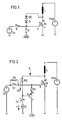
- Figure 1 shows a known circuit in which an inductive Consumer L in series with a low-side MOSFET switch M.
- the poles + Vbat and GND of an operating voltage source Vbat lies, the drain d with the consumer and the source s is connected to the negative pole GND.
- the positive pole + Vc connected to the gate g via a control switch S. is.
- the minus pole -Vc of the control voltage source Vc is with connected to the negative pole GND of the operating voltage source Vbat.
- the blocking diode D prevents when the MOSFET switch M is conductive, a current flows from the gate g the drain in this case at low potential d.
- the control switch is in the switched-off state of the circuit S opened and thus the MOSFET switch M is not conductive or high impedance; there is no current.
- Control switch S is closed to switch on the consumer and thus MOSFET switch M conductive. It flows in increasing current from the positive pole + Vbat via the consumer L and the MOSFET switch M to the negative pole GND. The consumer is switched on.
- Switch S is opened to switch off consumer L. and the gate g of the MOSFET switch M via the resistor R discharged.
- the potential at the drain d increases until it is reached a current through the Zener voltage of the Zener diode ZD Diodes ZD and D flow through which the gate g is recharged becomes. This creates a constant drain potential, until the coil L is demagnetized.
- FIG 2 shows a first schematic embodiment a switching device according to the invention, in which operating voltage source Vbat, consumer L, MOSFET switch M, Control voltage source Vc and control switch S1, as already described in Figure 1 are arranged.
- the control switch S1 here is a first resistor R5 connected in parallel.
- a clamping circuit K is provided instead of the Zener diode ZD. This consists of a second resistor R1, the a terminal connected to the gate g of the MOSFET switch M.
- switches S1 and S2 When switched off, switches S1 and S2 are open and the operating voltage source Vbat and the control voltage source Vc can in a manner not shown by the Circuit be separate and are at least during operation connected to her.
- Control switch S1 is closed to switch on the consumer and thus MOSFET switch M conductive. It flows in increasing current from the positive pole + Vbat via the consumer L and the MOSFET switch M to the negative pole GND. The consumer is switched on.
- Switch S1 is opened to switch off consumer L. and at the same time switch S2 closed.
- the constant current source Q flows from gate g through resistor R1, the Emitter base section of the pnp transistor T a current I1 to Negative pole GND, which controls the transistor T, whereby the gate g of the MOSFET switch M is discharged.
- the drain potential increases and an increasing part of the flows Current I1 from the drain d through the third resistor R2 in the Constant current source Q.
- transistor T becomes non-conductive again and the discharge gate g is interrupted.
- a voltage appears at the drain d during clamping one that essentially depends on the voltage Uk I1 * R2 across the resistor R2 depends. A small amount occurs via the resistor R5 Reloading the gate g. With the size of the resistance R1 the speed of the gate discharge can be determined. With the size of the resistor R2 and the current I1 can be the desired clamping voltage Uk - that of the Zener voltage corresponds to the circuit of Figure 1 - are set. This circuit can also be used for large clamping voltages the third resistor R2 easily into an IC usual technology can be integrated.
- FIG 3 is another schematic embodiment shown a switching device according to the invention, at which is also possible to chopper.
- this circuit there is one between the positive pole + Vbat and the negative pole GND of the operating voltage source Vbat Series connection of a consumer L and an electronic Lowside MOSFET switch M1 arranged. Between the gate g1 of the MOSFET switch M1 and the negative pole GND of the operating voltage source Vbat is a fourth resistor R6 and a series circuit in parallel with the fourth resistor R6 from a control switch S1 and a control voltage source Vc, whose negative pole -Vc with the negative pole GND of the operating voltage source Vbat is connected.
- Parallel to the consumer L is a series connection of a freewheeling diode D1 and one further MOSFET switch M2 arranged.
- the circuit first has a clamping circuit K1 with a second resistor R1, one of which is connected to the gate g2 of the further MOSFET switch M2 is connected. Furthermore a pnp transistor T1 is provided, the emitter e1 connected to the other terminal of the second resistor R1 and its collector c1 with the positive pole + Vbat Operating voltage source Vbat is connected.
- One on one sufficient to completely open the pnp transistor T1 and a constant current causing a desired clamping voltage Uk1 I1 set constant current source Q1 is on the one hand with the negative pole GND of the operating voltage source Vbat and on the other hand via a switch S2 with the base b1 of the pnp transistor T1 connected, and between the consumer L and the base of the pnp transistor T1 is a series connection a third resistor R2 and a blocking diode D2.
- Control switch S1 is closed to switch on the consumer and thus MOSFET switch M1 conductive. It flows in increasing current from the positive pole + Vbat via the consumer L and the MOSFET switch M1 to the negative pole GND.
- the consumer is switched on.
- the consumer can L e.g. by clocked operation of switch S1 with Reload a certain duty cycle (chopper mode), to maintain a certain consumer current receive.
- chopper operation takes over when switched off MOSFET switch M1 of the freewheeling circuit (freewheeling diode D1 and MOSFET switch M2) the current through the load L.
- the demagnetization time of an inductive consumer is determined by the voltage on it. In the circuits according to FIGS. 1 and 2, this voltage is in addition to the zener or clamping voltage also depends on the operating voltage Vbat.
- this dependence is removed from the operating voltage Vbat by using the Freewheeling circuit to an independent voltage (Ukl or Uk2) is clamped.
- Switch S1 is opened to demagnetize consumer L.
- switches S2 and S3 are closed.
- a current I1 flows from the gate g2 via R1-e2-b1-Q1 and a current I2 via R3-e2-b2-Q2 to GND and via Vbat to the negative pole -Vk and correspondingly increased currents flow I1 * v1 and I2 * v2 via R1-e1-c1 or via R3-e2-c2 to the negative pole -Vk, thereby discharging the gate g2 of the MOSFET switch M2 becomes.
- This increases the potential at drain d2 until at Reaching the clamping voltage Uk2 the total current I2 over the Resistor R4 flows and pnp transistor T2 is non-conductive becomes.
- the gate g2 becomes only one Current I1 * v1 cleared until the consumer demagnetizes is, which prevents large overshoots. becomes.
Landscapes
- Electronic Switches (AREA)
Description
- Figur 1:
- eine bekannte Vorrichtung zum Schalten eines induktiven Verbrauchers,
- Figur 2:
- ein erstes schematisches Ausführungsbeispiel einer erfindungsgemäßen Vorrichtung, und
- Figur 3:
- ein zweites schematisches Ausführungsbeispiel einer erfindungsgemäßen Vorrichtung.
Claims (5)
- Vorrichtung zum Schalten eines induktiven Verbrauchers (L), insbesondere eines Kraftstoffeinspritzventils einer Brennkraftmaschine,
mit einer zwischen dem Pluspol (+Vbat) und dem Minuspol (GND) einer Betriebsspannungsquelle (Vbat) liegenden Reihenschaltung aus dem Verbraucher (L) und einem elektronischen Lowside-MOSFET-Schalter (M),
mit einer zwischen dem Gate (g) des MOSFET-Schalters (M) und dem Minuspol (GND) der Betriebsspannungsquelle (Vbat) liegenden Reihenschaltung aus einem Steuerschalter (S1) und einer Steuerspannungsquelle (Vc), deren Minuspol (-Vc) mit dem Minuspol (GND) der Betriebsspannungsquelle (Vbat) verbunden ist,
mit einem dem Steuerschalter (S1) parallelgeschalteten ersten Widerstand (R5), und
mit einer Klemmschaltung (K), bestehend aus:einem zweiten Widerstand (R1), dessen einer Anschluß mit dem Gate (g) des MOSFET-Schalters (M) verbunden ist,einem pnp-Transistor (T), dessen Emitter (e) mit dem anderen Anschluß des zweiten Widerstandes (R1) verbunden ist, und dessen Kollektor (c) mit dem Minuspol (GND) der Betriebsspannungsquelle (Vbat) verbunden ist,einer Konstantstromquelle (Q), die einerseits mit dem Minuspol (GND) und andererseits über einen Schalter (S2) mit der Basis (b) des pnp-Transistors (T) verbunden ist, undeinem dritten Widerstand (R2), der einerseits mit der Basis (b) des pnp-Transistors (T) und andererseits mit dem Drain (d) des MOSFET-Schalters (M) verbunden ist. - Vorrichtung zum Schalten eines induktiven Verbrauchers (L), insbesondere eines Kraftstoffeinspritzventils einer Brennkraftmaschine,
mit einer zwischen dem Pluspol (+Vbat) und dem Minuspol (GND) einer Betriebsspannungsquelle (Vbat) liegenden Reihenschaltung aus dem Verbraucher (L) und einem elektronischen Lowside-MOSFET-Schalter (M1),
mit einem zwischen dem Gate (g1) des MOSFET-Schalters (M1) und dem Minuspol (GND) der Betriebsspannungsquelle (Vbat) liegenden vierten Widerstand (R6) und mit einer parallel zum vierten Widerstand (R6) liegenden Reihenschaltung aus einem Steuerschalter (S1) und einer Steuerspannungsquelle (Vc), deren Minuspol (-Vc) mit dem Minuspol (GND) der Betriebsspannungsquelle (Vbat) verbunden ist,
mit einer parallel zum Verbraucher (L) angeordneten Reihenschaltung aus einer Freilaufdiode (D1) und einem weiteren MOSFET-Schalter (M2),
mit einer weiteren Spannungsquelle (Vk), deren Minuspol (-Vk) mit der Source (s2) des weiteren MOSFET-Schalters (M2) und mit dem Pluspol (+Vbat) der Betriebsspannungsquelle (Vbat) verbunden ist und deren Pluspol (+Vk) über einen ersten Widerstand (R5) mit dem Gate (g2) des weiteren MOSFET-Schalters (M2) verbunden ist, und
mit einer ersten Klemmschaltung(K1), bestehend aus:einem zweiten Widerstand (R1), dessen einer Anschluß mit dem Gate (g2) des weiteren MOSFET-Schalters (M2) verbunden ist,einem ersten pnp-Transistor (T1), dessen Emitter (e1) mit dem anderen Anschluß des zweiten Widerstandes (R1) verbunden ist, und dessen Kollektor (c1) mit dem Pluspol (+Vbat) der Betriebsspannungsquelle (Vbat) verbunden ist,einer ersten Konstantstromquelle (Q1), die einerseits mit dem Minuspol (GND) der Betriebsspannungsquelle (Vbat) und andererseits über einen ersten Schalter (S2) mit der Basis (b1) des ersten pnp-Transistors (T1) verbunden ist, undeiner Reihenschaltung aus einem dritten Widerstand (R2), der einerseits mit dem Verbraucher verbunden ist, und einer ersten Sperrdiode (D2), die mit der Basis (b1) des ersten pnp-Transistors (T1) verbunden ist. - Vorrichtung nach Anspruch 2, dadurch gekennzeichnet, daß parallel zur ersten Klemmschaltung (K1) eine zweite Klemmschaltung (K2) angeordnet ist, bestehend aus:einem fünften Widerstand (R3), dessen einer Anschluß mit dem Gate (g2) des weiteren MOSFET-Schalters (M2) verbunden ist,einem zweiten pnp-Transistor (T2), dessen Emitter (e2) mit dem anderen Anschluß des fünften Widerstandes (R3) verbunden ist, und dessen Kollektor (c2) mit dem Pluspol (+Vbat) der Betriebsspannungsquelle (Vbat) verbunden ist,einer zweiten Konstantstromquelle (Q2), die einerseits mit dem Minuspol (GND) der Betriebsspannungsquelle (Vbat) und andererseits über einen zweiten Schalter (S3) mit der Basis (b2) des zweiten pnp-Transistors (T2) verbunden ist, undeiner Reihenschaltung aus einem sechsten Widerstand (R4), der einerseits mit dem Verbraucher (L) verbunden ist, und einer zweiten Sperrdiode (D4), die mit der Basis (b2) des zweiten pnp-Transistors (T2) verbunden ist.
- Vorrichtung nach Anspruch 3, dadurch gekennzeichnet, daß die beiden Klemmschaltungen (K1, K2) so dimensioniert sind, daß unterschiedliche Klemmspannungen Uk1 > Uk2 entstehen, mit Uk1 = I1*R2, Uk2 = I2*R4 und mit R3 < R1, wobei R2 der dritte Widerstand, R4 der sechste Widerstand, I1 der Strom der ersten Konstantstromquelle (Q1), I2 der Strom der zweiten Konstantstromquelle (Q2), R3 der fünfte Widerstand und R1 der zweite Widerstand ist.
- Vorrichtung nach Anspruch 3, dadurch gekennzeichnet, daß eine von der Basis (b2) des zweiten pnp-Transistors (T2) zum Gate (g2) des weiteren MOSFET-Schalters (M2) stromdurchlässige dritte Sperrdiode (D3) vorgesehen ist.
Applications Claiming Priority (2)
| Application Number | Priority Date | Filing Date | Title |
|---|---|---|---|
| DE19626630 | 1996-07-02 | ||
| DE19626630A DE19626630C1 (de) | 1996-07-02 | 1996-07-02 | Vorrichtung zum Schalten eines induktiven Verbrauchers |
Publications (3)
| Publication Number | Publication Date |
|---|---|
| EP0817380A2 EP0817380A2 (de) | 1998-01-07 |
| EP0817380A3 EP0817380A3 (de) | 1999-07-28 |
| EP0817380B1 true EP0817380B1 (de) | 2003-08-20 |
Family
ID=7798721
Family Applications (1)
| Application Number | Title | Priority Date | Filing Date |
|---|---|---|---|
| EP97109602A Expired - Lifetime EP0817380B1 (de) | 1996-07-02 | 1997-06-12 | Vorrichtung zum Schalten eines induktiven Verbrauchers |
Country Status (4)
| Country | Link |
|---|---|
| US (1) | US5828141A (de) |
| EP (1) | EP0817380B1 (de) |
| KR (1) | KR100438457B1 (de) |
| DE (2) | DE19626630C1 (de) |
Families Citing this family (12)
| Publication number | Priority date | Publication date | Assignee | Title |
|---|---|---|---|---|
| US6078204A (en) * | 1996-12-19 | 2000-06-20 | Texas Instruments Incorporated | High current drain-to-gate clamp/gate-to-source clamp for external power MOS transistors |
| US5909135A (en) * | 1996-12-19 | 1999-06-01 | Texas Instruments Incorporated | High-side MOSFET gate protection shunt circuit |
| JP2002246551A (ja) * | 2001-02-15 | 2002-08-30 | Hitachi Ltd | 半導体装置 |
| DE10117356B4 (de) * | 2001-04-07 | 2006-09-07 | Robert Bosch Gmbh | Schaltungsanordnung |
| DE102004013599A1 (de) * | 2004-03-19 | 2005-10-06 | Robert Bosch Gmbh | Ansteuerschaltung zum Ansteuern einer leistungselektronischen Schaltung sowie Verfahren hierzu |
| DE102006036349B4 (de) * | 2006-08-03 | 2015-04-02 | Infineon Technologies Ag | Schaltungsvorrichtung und Verfahren zum Erkennen eines Betriebszustandes |
| DE102008033138A1 (de) * | 2008-07-15 | 2010-01-21 | Continental Automotive Gmbh | Schaltungsanordnung zum Schalten einer induktiven Last |
| US7868683B2 (en) * | 2008-08-12 | 2011-01-11 | Infineon Technologies Ag | Switch using an accelerating element |
| DE102009007790B3 (de) * | 2009-02-06 | 2010-08-12 | Continental Automotive Gmbh | Treiberchip zum Treiben einer induktiven Last |
| CN102545852B (zh) * | 2012-01-17 | 2013-12-18 | 南京航空航天大学 | 应用于固态功率控制器的泄漏钳位电路及其控制方法 |
| JP5875426B2 (ja) * | 2012-03-22 | 2016-03-02 | 富士通テン株式会社 | センサ信号処理装置、および車載型電子制御装置 |
| DE102017202184A1 (de) * | 2017-02-13 | 2018-08-16 | Robert Bosch Gmbh | Schaltungsanordnung zum Erhöhen der Freilaufspannung einer induktiven Last und Endstufe |
Family Cites Families (8)
| Publication number | Priority date | Publication date | Assignee | Title |
|---|---|---|---|---|
| DE3109650A1 (de) * | 1981-03-13 | 1982-09-23 | Robert Bosch Gmbh, 7000 Stuttgart | "aus einer induktiven last und der anoden-kathoden-strecke eines selbstsperrenden feldeffekttransistors bestehende serienschaltung" |
| DE3132257C2 (de) * | 1981-08-14 | 1983-10-20 | Siemens AG, 1000 Berlin und 8000 München | Überlastungsschutzschaltung für einen Feldeffekttransistor |
| US4893211A (en) * | 1985-04-01 | 1990-01-09 | Motorola, Inc. | Method and circuit for providing adjustable control of short circuit current through a semiconductor device |
| US5266840A (en) * | 1988-10-25 | 1993-11-30 | Siemens Aktiengesellschaft | Circuit for detecting the failure of a load which is connected in series with an electronic switch |
| US5272399A (en) * | 1992-02-25 | 1993-12-21 | Siemens Aktiengesellschaft | Circuit limiting the load current of a power MOSFET |
| ES2101148T3 (es) * | 1992-03-10 | 1997-07-01 | Siemens Ag | Circuito de proteccion para un mosfet de potencia, que acciona una carga inductiva. |
| JPH0894695A (ja) * | 1994-09-27 | 1996-04-12 | Mitsubishi Electric Corp | 半導体パワースイッチシステム |
| DE19609121C1 (de) * | 1996-03-08 | 1997-02-27 | Siemens Ag | Schaltungsanordnung zum Ansteuern eines Feldeffekttransistors mit sourceseitiger Last |
-
1996
- 1996-07-02 DE DE19626630A patent/DE19626630C1/de not_active Expired - Fee Related
-
1997
- 1997-06-12 DE DE59710603T patent/DE59710603D1/de not_active Expired - Fee Related
- 1997-06-12 EP EP97109602A patent/EP0817380B1/de not_active Expired - Lifetime
- 1997-07-02 KR KR1019970030567A patent/KR100438457B1/ko not_active Expired - Fee Related
- 1997-07-02 US US08/887,470 patent/US5828141A/en not_active Expired - Fee Related
Also Published As
| Publication number | Publication date |
|---|---|
| KR100438457B1 (ko) | 2004-07-16 |
| EP0817380A3 (de) | 1999-07-28 |
| US5828141A (en) | 1998-10-27 |
| DE59710603D1 (de) | 2003-09-25 |
| DE19626630C1 (de) | 1997-09-11 |
| EP0817380A2 (de) | 1998-01-07 |
| KR980012894A (ko) | 1998-04-30 |
Similar Documents
| Publication | Publication Date | Title |
|---|---|---|
| DE69420327T2 (de) | Halbleiter-Leistungsschaltung | |
| DE69509737T2 (de) | Bidirektionaler Trennschalter für eine Batterie | |
| DE10046668B4 (de) | Elektrische Lastansteuerungsschaltung mit Schutzeinrichtung | |
| EP0423885B1 (de) | Stromversorgungseinrichtung mit Einschaltstrombegrenzungsschaltung | |
| DE19628131C2 (de) | Gatespannungsbegrenzung für eine Schaltungsanordnung | |
| DE68905360T2 (de) | Steuerschaltung für eine induktive Last. | |
| WO2010108292A2 (de) | Schalteinrichtung mit einer kaskodeschaltung | |
| DE102014108576B4 (de) | Treiberschaltung mit Miller-Clamping-Funktionalität für Leistungshalbleiterschalter, Leistungshalbleiterschalter und Wechselrichterbrücke | |
| EP0620957B1 (de) | Schaltung zum schutz eines mosfet-leistungstransistors | |
| DE102009007790B3 (de) | Treiberchip zum Treiben einer induktiven Last | |
| EP0817380A2 (de) | Vorrichtung zum Schalten eines induktiven Verbrauchers | |
| DE102006015024B3 (de) | Treiberschaltung zum Bereitstellen eines Ausgangssignals | |
| DE68924107T2 (de) | Steuerschaltung für die Begrenzungsspannung einer durch eine Leistungsvorrichtung in spannungsseitiger Treiberkonfiguration getriebenen induktiven Last. | |
| DE19619399A1 (de) | Schaltvorrichtung mit einem Leistungs-FET und einer induktiven Last | |
| DE3741394C2 (de) | Schaltungsanordnung zum Schutz vor Verpolungsschäden für Lastkreise mit einem MOS-FET als Schalttransistor | |
| DE102018117528A1 (de) | Entladeschaltungen zum Entladen von induktiven Elementen mit Temperaturschutz | |
| WO2006134009A1 (de) | Schaltungsanordnung zum schalten einer last | |
| EP2466753A1 (de) | Widerstandsschaltung, Schaltungsanordnung und Treiber | |
| DE10143432C1 (de) | Treiberschaltung und Ansteuerverfahren für einen feldgesteuerten Leistungsschalter | |
| WO1997030481A1 (de) | Integrierte schaltungsanordnung zum ansteuern eines leistungs-mosfet mit sourceseitiger last | |
| DE19838109B4 (de) | Ansteuerschaltung für induktive Lasten | |
| DE102016210798B3 (de) | Leistungshalbleiterschaltung | |
| DE3536447C2 (de) | Kurzschluß- und überlastfeste Transistorausgangsstufe | |
| DE102016204384A1 (de) | Hauptschalter mit Verpolschutz | |
| DE102008060793B4 (de) | Schaltungsanordnung zum Schalten einer oder mehrerer induktiver Lasten |
Legal Events
| Date | Code | Title | Description |
|---|---|---|---|
| PUAI | Public reference made under article 153(3) epc to a published international application that has entered the european phase |
Free format text: ORIGINAL CODE: 0009012 |
|
| AK | Designated contracting states |
Kind code of ref document: A2 Designated state(s): DE FR GB IT |
|
| PUAL | Search report despatched |
Free format text: ORIGINAL CODE: 0009013 |
|
| AK | Designated contracting states |
Kind code of ref document: A3 Designated state(s): AT BE CH DE DK ES FI FR GB GR IE IT LI LU MC NL PT SE |
|
| 17P | Request for examination filed |
Effective date: 19991217 |
|
| AKX | Designation fees paid |
Free format text: DE FR GB IT |
|
| GRAH | Despatch of communication of intention to grant a patent |
Free format text: ORIGINAL CODE: EPIDOS IGRA |
|
| GRAH | Despatch of communication of intention to grant a patent |
Free format text: ORIGINAL CODE: EPIDOS IGRA |
|
| GRAA | (expected) grant |
Free format text: ORIGINAL CODE: 0009210 |
|
| AK | Designated contracting states |
Designated state(s): DE FR GB IT |
|
| REG | Reference to a national code |
Ref country code: GB Ref legal event code: FG4D Free format text: NOT ENGLISH |
|
| GBT | Gb: translation of ep patent filed (gb section 77(6)(a)/1977) | ||
| REF | Corresponds to: |
Ref document number: 59710603 Country of ref document: DE Date of ref document: 20030925 Kind code of ref document: P |
|
| ET | Fr: translation filed | ||
| PG25 | Lapsed in a contracting state [announced via postgrant information from national office to epo] |
Ref country code: GB Free format text: LAPSE BECAUSE OF NON-PAYMENT OF DUE FEES Effective date: 20040612 |
|
| PLBE | No opposition filed within time limit |
Free format text: ORIGINAL CODE: 0009261 |
|
| STAA | Information on the status of an ep patent application or granted ep patent |
Free format text: STATUS: NO OPPOSITION FILED WITHIN TIME LIMIT |
|
| 26N | No opposition filed |
Effective date: 20040524 |
|
| GBPC | Gb: european patent ceased through non-payment of renewal fee |
Effective date: 20040612 |
|
| PG25 | Lapsed in a contracting state [announced via postgrant information from national office to epo] |
Ref country code: IT Free format text: LAPSE BECAUSE OF NON-PAYMENT OF DUE FEES;WARNING: LAPSES OF ITALIAN PATENTS WITH EFFECTIVE DATE BEFORE 2007 MAY HAVE OCCURRED AT ANY TIME BEFORE 2007. THE CORRECT EFFECTIVE DATE MAY BE DIFFERENT FROM THE ONE RECORDED. Effective date: 20050612 |
|
| PGFP | Annual fee paid to national office [announced via postgrant information from national office to epo] |
Ref country code: FR Payment date: 20090615 Year of fee payment: 13 |
|
| PGFP | Annual fee paid to national office [announced via postgrant information from national office to epo] |
Ref country code: DE Payment date: 20090630 Year of fee payment: 13 |
|
| REG | Reference to a national code |
Ref country code: FR Ref legal event code: ST Effective date: 20110228 |
|
| PG25 | Lapsed in a contracting state [announced via postgrant information from national office to epo] |
Ref country code: DE Free format text: LAPSE BECAUSE OF NON-PAYMENT OF DUE FEES Effective date: 20110101 |
|
| PG25 | Lapsed in a contracting state [announced via postgrant information from national office to epo] |
Ref country code: FR Free format text: LAPSE BECAUSE OF NON-PAYMENT OF DUE FEES Effective date: 20100630 |