EP0817054A2 - Antémémoire à double écriture simultanée - Google Patents
Antémémoire à double écriture simultanée Download PDFInfo
- Publication number
- EP0817054A2 EP0817054A2 EP97110131A EP97110131A EP0817054A2 EP 0817054 A2 EP0817054 A2 EP 0817054A2 EP 97110131 A EP97110131 A EP 97110131A EP 97110131 A EP97110131 A EP 97110131A EP 0817054 A2 EP0817054 A2 EP 0817054A2
- Authority
- EP
- European Patent Office
- Prior art keywords
- cache
- controller
- modules
- data
- quadrants
- Prior art date
- Legal status (The legal status is an assumption and is not a legal conclusion. Google has not performed a legal analysis and makes no representation as to the accuracy of the status listed.)
- Withdrawn
Links
Images


Classifications
-
- G—PHYSICS
- G06—COMPUTING; CALCULATING OR COUNTING
- G06F—ELECTRIC DIGITAL DATA PROCESSING
- G06F11/00—Error detection; Error correction; Monitoring
- G06F11/07—Responding to the occurrence of a fault, e.g. fault tolerance
- G06F11/16—Error detection or correction of the data by redundancy in hardware
- G06F11/20—Error detection or correction of the data by redundancy in hardware using active fault-masking, e.g. by switching out faulty elements or by switching in spare elements
- G06F11/2053—Error detection or correction of the data by redundancy in hardware using active fault-masking, e.g. by switching out faulty elements or by switching in spare elements where persistent mass storage functionality or persistent mass storage control functionality is redundant
- G06F11/2056—Error detection or correction of the data by redundancy in hardware using active fault-masking, e.g. by switching out faulty elements or by switching in spare elements where persistent mass storage functionality or persistent mass storage control functionality is redundant by mirroring
- G06F11/2087—Error detection or correction of the data by redundancy in hardware using active fault-masking, e.g. by switching out faulty elements or by switching in spare elements where persistent mass storage functionality or persistent mass storage control functionality is redundant by mirroring with a common controller
-
- G—PHYSICS
- G11—INFORMATION STORAGE
- G11C—STATIC STORES
- G11C29/00—Checking stores for correct operation ; Subsequent repair; Testing stores during standby or offline operation
- G11C29/70—Masking faults in memories by using spares or by reconfiguring
- G11C29/74—Masking faults in memories by using spares or by reconfiguring using duplex memories, i.e. using dual copies
-
- G—PHYSICS
- G06—COMPUTING; CALCULATING OR COUNTING
- G06F—ELECTRIC DIGITAL DATA PROCESSING
- G06F12/00—Accessing, addressing or allocating within memory systems or architectures
- G06F12/02—Addressing or allocation; Relocation
- G06F12/08—Addressing or allocation; Relocation in hierarchically structured memory systems, e.g. virtual memory systems
- G06F12/0802—Addressing of a memory level in which the access to the desired data or data block requires associative addressing means, e.g. caches
- G06F12/0866—Addressing of a memory level in which the access to the desired data or data block requires associative addressing means, e.g. caches for peripheral storage systems, e.g. disk cache
Definitions
- the present invention relates to writing duplicate entries in separate cache locations simultaneously whereby cache entries are mirrored, or written twice, in one write cycle resulting in physically separate and independent copies of the data.
- cache memory stores frequently accessed data word units in cache memory as well as in primary memory.
- the storage system must maintain data coherence between the word unit in cache and the same word unit in primary storage.
- write-through cache the processor writes the modified word unit to both the cache and primary memory to ensure that both memories always have updated copies of the word unit. This is the simplest and most commonly used method.
- write-back cache the cache controller keeps track of which word units in the cache have been modified by the processor. This is done by marking the modified word units with a dirty bit. Thereafter, when word units are displaced from the cache, the word units with a dirty bit are written to primary memory.
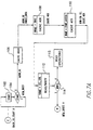
- FIG. 1 shows an example of the conventional mirror write system.
- Cache system 10 contains controller 10A and cache 10B
- cache system 12 contains controller 12A and cache 12B.
- the cache systems are interconnected by bus 14.
- a review of the mirror write operation in Fig. 1 illustrates how slow the operation is in the prior art.
- a mirror write in Fig. 1 begins with a write request to either cache system. Assume a mirror write request is received at cache system 12. Controller 12A writes the word unit into cache 12B. Controller 12A then reads the word unit to cache system 10 over bus 14. Controller 10A then writes the word unit to cache 10B. After the word unit is successfully written to cache 10B, controller 10A sends an acknowledge signal back to cache system 12. Cache system 12 receives the acknowledge and sends it back to the processor. Accordingly, the mirror write in the conventional system requires in sequence a write operation, a read operation, a second write operation, and two successive acknowledge operations. In addition, if bus 14 is shared with other storage devices in addition to the two cache systems, there may be a delay in communications between cache systems 10 and 12.
- the mirror write has not solved the second problem of access to data if a controller in one cache system and a cache in the other cache system fails. For example, if controller 10A fails, data in cache 10B is not available. If cache 12B goes bad in this situation, the data is lost unless controller 12A can get to the data in cache 10B through a second cycle using bus 14.
- the present invention in its broad form, resides in apparatus and method for mirror writing in a cache memory system as recited in claims 1 and 7 respectively.
- a preferred embodiment of this invention provides a cache memory system in a computing system where the cache memory system has a first cache module storing data, a second cache module storing data, and a controller writing data simultaneously to both the first and second cache modules.
- a second controller can be added to also write data simultaneously to both the first and second cache modules.
- each controller requests access to both of the first and second cache modules.
- Both cache modules send an acknowledgment of the cache request back to the controllers.
- Each controller in response to the acknowledgments from both of the cache modules simultaneously sends the same data to both cache modules.
- Both of the cache modules write the same data into cache in their respective cache modules.
- a combination of the cache memories is split into quadrants, Q0, Q1, Q2 and Q3 with quadrants Q0 and Q1 in one cache memory and quadrants Q2 and Q3 in the other cache memory.
- One controller simultaneously writes the same data to both quadrants Q0 and Q3, and the other controller simultaneously writes the same data to both quadrants Q1 and Q2.
- the controller detecting failure of the other controller sends accesses to quadrants previously accessed by the failed controller.
- the great advantage realized herein is the simultaneous mirror writing of the same data to two cache memories in a single write cycle. Another advantage is the reliability achieved with each of the controllers having access to both cache memories.
- FIG. 2 A preferred embodiment of two coordinated cache systems in accordance with the invention is shown in Fig. 2.
- the two cache memories, Cache A and Cache B, are divided in half by addressing. Accordingly, the total cache memory may be viewed as four quadrants of cache, quadrants Q0 and Q1 are in Cache A and quadrants Q2 and Q3 are in Cache B. In an alternate embodiment the cache quadrants are not necessarily the same size.
- the cache storage system has two controllers. Controller 20, writes word units simultaneously to quadrant Q0 of Cache A and quadrant Q3 of Cache B. This write operation is not two successive writes, but is two simultaneous write operations in parallel, one to quadrant Q0 and the second to quadrant Q3. The same base address is used in both quadrants. Alternatively, address translation may be used to place the mirror data at different addresses in the mirror quadrants.
- second controller 22 whenever second controller 22 has data to write to cache, it simultaneously writes that data word unit to quadrant Q1 in Cache A and quadrant Q2 in Cache B.
- the mirror write operation of a single word unit to two separate cache memories is done as one write operation in parallel to two caches.
- This configuration of a cache storage system accomplishes a mirror cache write and writes the two word units several times faster than the conventional mirror write cache system in Fig. 1. This is due to the fact that there is only one write operation in contrast to the prior art where there was a write operation followed by a read operation followed by a write operation.
- Controller 20 and controller 22 have the capability of writing and reading any of the quadrants in cache A and cache B. Further, Controller 20 and controller 22 are communicating and know each other's status of operation. Thus, if controller 20 fails, controller 22 can still simultaneously write to two quadrants and read any word unit entry in any quadrant of the cache memories. Accordingly if a controller fails, the simultaneous mirror write function is still operational, and there is no combination of cache memory loss and controller loss that prevents reading of data from a remaining good cache quadrant.
- Fig. 3A another preferred embodiment of the invention where the switching of the address data bus connection to the quadrants in the cache modules is done at the cache modules under control of signals from the controllers.
- Fig. 3A illustrates the normal mirrored write operation in accordance with this preferred embodiment of the invention.
- Controllers 20 and 22 and Cache A Module 21 and Cache B Module 23, along with the connections between each of these components are mirror images of each other.
- controller 20 is referred to herein as "THIS” controller
- controller 22 is referred to as "OTHER" controller.
- Control Line 27 is a hard reset or kill line whereby either controller 20 or controller 22 may hard reset or kill the other controller.
- Control Lines 29, 31, 33 and 35 are lock lines that lock the operation of Cache A Module 21 and Cache B Module 23.
- Control Line 29 is the THIS Locks A (TLA) control line. This occurs when the signal on Control Line 29 is high, or in a binary 1 state.
- Control Line 31 is the TLB line, i.e. THIS Locks B control line.
- Control Line 33 is the OLA, OTHER Locks A control line.
- Control Line 35 is the OLB or OTHER locks B control line. In a normal mirror write operation, all of these control lines 29, 31, 33 and 35 are high or in a binary 1 state as indicated in Fig. 3A.
- Control lines 41 pass requests, acknowledgment, read/write state and sync signals between THIS controller 20 and Cache A Module 21 and Cache B Module 23.
- Control lines 43 similarly pass request, acknowledge, read/write and sync signals between OTHER controller 22 and Cache A Module 21 and Cache B Module 23.
- Address data bus 40 passes the address and subsequently data words from THIS controller 20 to Cache A Module 21 and Cache B Module 23.
- Address data bus 45 similarly passes address and data words from OTHER controller 22 to Cache B Module 23 and Cache A Module 21.
- switch 47 In each of the Cache Modules, 21 and 23, there is a switch between the address/data buses 40 and 45 and the quadrants of the cache module.
- switch 47 In Cache A Module 21, switch 47 directs address/data bus 40 to Quadrant Q0 and address/data bus 45 to Quadrant Q1.
- Switch 47 is controlled by the TLA and TLB lock signals. In the mirror write operation both of these lock signals are high or in a binary 1 state.
- Switch 49 in Cache B Module 23 is also in a mirror write condition due to the binary 1 inputs from the OLA and the OLB control Lines 33 and 35. Accordingly, switch 49 connects address/data bus 45 to Quadrant Q2 and connects address/data bus 40 to Quadrant Q3.
- the invention can still perform mirror write operations even though one controller crashes.
- Fig. 3B this fail-safe operation is illustrated where OTHER controller 22 has failed.
- THIS controller 20 and OTHER controller 22 carry on a keep-alive and status conversation over message link 25. For example, periodically THIS controller 20 will send a "keep alive" message over link 25 to OTHER controller 22. OTHER controller 22 will respond with a status message back across link 25 to THIS controller 20. If THIS controller 20 detects the absence of a status message back from OTHER controller 22, controller 20 assumes OTHER controller 22 is failing or has failed.
- THIS controller 20 then generates a kill or hard reset signal on line 27 to kill operations by OTHER controller 22.
- Each of the Cache Modules 21 and 23 will receive a binary 1 control signal from TLA and TLB respectively and a binary 0 signal from OLA and OLB respectively. This 1 and 0 condition added to the Cache Modules 21 and 23 will change the state of switches 47 and 49.
- THIS controller 20 When THIS controller 20 is using an address with a most significant digit being a 6 THIS controller will simultaneously write to Q0 through switch 47 and to Q3 through switch 49.
- THIS controller 20 is using an address 7 for the most significant hexadecimal digit, THIS controller will simultaneously write to Q1 through switch 47 and to Q2 through switch 49. Notice that in both cases the address and data information for the cache modules comes over address data bus 40.
- OTHER controller 22 can do a mirror write if THIS controller 20 fails. In such a situation, TLA and TLB would go low and OLA and OLB would go high. For a most significant digit 6 in the address at OTHER controller 22, bus 45 would be connected by switch 47 to quadrant Q1 and to Quadrant Q2 through switch 49. For an address 7 in the most significant digit position, OTHER controller 22 will route the data through bus 45 through switch 47 to Quadrant Q0 and through bus 45 through switch 49 to Quadrant Q3.
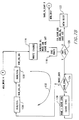
- Fig. 4 illustrates, in more detail, one-half of the cache system in Fig. 3A.
- controller 20 is illustrated along with quadrant Q0 of Cache Module 0 (CACHE A) and quadrant Q3 in Cache Module 1 (CACHE B).
- Controller 22, working with quadrants Q1 and Q2 in Cache Modules 0 and 1 respectively, would have the same elements as will now be described for controller 20 and cache quadrants Q0 and Q3.
- the mirror write operation begins with the controller state machine 24 sending a CACHE REQ (cache request) 0 signal over line 26 to sync logic 28 in CACHE MODULE 0.
- controller state machine 24 generates the CACHE REQ 1 signal, which goes out over line 30 to sync logic 32 in CACHE MODULE 1.
- the CACHE REQ 0 and CACHE REQ 1 are shown in the timing diagram illustrated in Fig. 5.
- the top signal line is the cache address/data signal indicating the timing of address and data information on the CDAL (cache data/address line) bus 40 in Fig. 4.
- the CACHE REQ 0 and CACHE REQ 1 signals are represented by a transition from high to low on the signal lines correspondingly labeled in Fig. 5. These transitions occur during a time when the address is on the CDAL bus 40 in Fig. 4. Transition 42 of the CACHE REQ 0 signal notifies CACHE MODULE 0 to read the address on bus 40. Likewise, transition 44 in CACHE REQ 1 signal notifies CACHE MODULE 1 to read the cache address on bus 40.
- the cache request transitions 42 and 44 also signal the cache modules to sample the state of the cache read write/sync signal in Fig. 5.
- the read write/sync signal is high to indicate a write and low to indicate a read. As shown in the mirror write example in Fig. 5, the read write/sync signal is high at the time of request transitions 42 and 44. Therefore, both cache modules 0 and 1 will know that data is to be written at the address just received.
- each cache state machine, 37 or 38 accepts the DATA 0 word unit 39 from CDAL bus 40, the cache state machine generates an acknowledgment signal, CACHE ACK 0 or CACHE ACK 1.
- CACHE ACK 0 goes back from cache state machine 37 to the sync and latch logic 46 in controller 20.
- CACHE ACK 1 goes back from cache state machine 38 to the sync and latch logic 46 and controller 20.
- the CACHE ACK 0 and CACHE ACK 1 signals are not necessarily generated at the same time.
- AND 48 will generate an output indicating both cache modules 0 and 1 have acknowledged receipt of the first word unit.
- This output goes to the controller state machine 24 which then drops or transitions the CACHE RW/SYNCH signal (Fig. 5) from high level to low level.
- This transition 50 of the CACHE RW/SYNCH signal in Fig. 5 is the sync signal passed from the controller state machine back to the cache state machines 37 and 38. This sync signal tells the cache state machines that DATA 1 word unit is now on the CDAL bus 40.
- the data on the CDAL bus is in four data words, data 0, data 1, data 2 and data 3 as shown in Fig. 5.
- the data is received and written by the cache modules starting at the address just previously received over the CDAL bus and in sequential addresses after the starting address.
- the controller state machine raises the CACHE REQ 0 and CACHE REQ 1 signal back to the high level to indicate the end of the current write cycle.
- the cache state machines are prompted to acknowledge that the last data is being received. Accordingly, a CACHE ACK 0 pulse 56 and a CACHE ACK 1 pulse 58 are sent back from the cache state machines to the controller 20 to acknowledge receipt of data.
- Fig. 6 composed of Figs. 6A and 6B, illustrates the details of the controller state machine 24 of Fig. 4.
- the state machine advances from state to state on each clock tick from the local clock in the controller.
- some states have a decision operation to detect the presence of a condition before action is taken and an advance is made to the next state. The action taken is indicated at the output path of the state or the decision operation.
- start state 51 cooperates with start decision operation 53 to detect an access request.
- the access request is generated by the controller microprocessor in response to an access request from the host.
- start state 51 causes decision operation 53 to test for an access request. If there is no access request, decision operation 53 indicates memory is busy, and the operation flow returns to start state 51. If there is an access request detected, decision operation 53 generates a CDAL ADDR (cache data/address line address) enable signal to put the address for the access request on the CDAL bus 40 (Fig. 4). The operation flow then passes to CDAL enable state 55 on the next clock tick.
- CDAL ADDR cache data/address line address
- CDAL enable state 55 keeps the CDAL ADDR enable signal asserted.
- cache request state 57 On the next clock tick cache request state 57 generates the cache request signals (CACHE_REQ 0 and CACHE_REQ 1 in Figs 4 and 5). In other words the cache request signals go through a transition from high to low. Cache request state 57 also continues to assert the CDAL enable signal.
- Cache access states 59, 61, 63 and 65 are advanced through in turn in the next successive four clock ticks. Each of these states maintains the CDAL ADDR enable signal and the cache request signals.
- Cache access state 65 also has a decision operation 66 that tests whether the access request is a read or write request. If the request is a read request the operation flow branches to cache read operations 67 which are not a part of the present invention and not shown in detail. If the request is a write request, the CDAL enable signal and the CACHE REQ signal is generated. The continued assertion of CACHE REQ indicates there is a cache write request and the last word unit to be written in this write cycle has not been reached yet. The operation flow branches to CDAL DATA enable state 68 when the next clock tick occurs.
- CDAL DATA enable state 68 generates the CDAL DATA enable signal to put data unit words on the CDAL bus 40 (Fig. 4). State 68 also maintains the cache request signals. For each clock tick after state 68 the controller state machine advances through write states 70, 72 and 74. Accordingly, for these three clock ticks these states maintain the CACHE REQ signal and the CDAL DATA enable signal.
- decision operation 76 tests whether the controller has received back both CACHE ACK 0 and 1 signals and whether the data word unit to be written is the last unit in this write cycle to be written. If both of these conditions are satisfied, this indicates that both cache modules have acknowledged the write request and that the controller is sending only one word unit to be written rather than a burst of four word units. If either of the conditions is not satisfied, the operation flow branches to decision operation 77. Decision operation 77 is testing for receipt of both CACHE ACK 0 and 1 signals and the not last data word unit, i.e. both cache modules have replied and a burst of data word units is to be written. If both decision operation 76 and 77 branch false, then the CACHE ACK signals must not been received by the controller. Accordingly, the operation flow branches false back to the input of write ACK state 74.
- the operation flow branches true from decision operation 76 to decision operation 78 when both CACHE ACKs have been received and only one data word unit has been written.
- Decision operation 78 tests whether the word unit to be written is not the last word unit to be written. Since decision operation 76 just indicated or detected that it was the last word unit to be written, the operation flow will branch false from decision operation 78 to state 80 while maintaining the CDAL data enable condition.
- cache write states 80 and 82 maintain the CDAL DATA enable condition.
- cache write state 84 clears the cache select and the cache request to prepare for the next access cycle. The operation flow then returns to the start state 50 in Fig. 6A.
- the operation flow branches true from decision operation 77 to operation 86 when both CACHE ACKs have been received and a burst of four data word units is to be written.
- Write sync states 86 and 88 continue to maintain the CDAL data enable and the cache request signal for the next two clock ticks.
- decision operation 78 is again used to check for the not last condition of the data word units being sent of the CDAL bus. If the controller indicates the data word unit is not the last to be written (burst operation), then the operation flow branches true from decision operation 78 and the operation maintains the CACHE REQ signal the CDAL enable and increments the burst counter.
- the burst counter will count the number of passes through the true state detection condition of decision operation 78 so as to detect when the last data word of a burst of data words in the write cycle has been placed on the CDAL bus 40. Thereafter at each clock tick the operation flow advances through cache write states 90, 92, 94, 96, 98, and 100 successively. Each of these cache write states maintains the cache request signal in the CDAL data bus enable condition. Thus, for the next six clock ticks these conditions are maintained.
- a burst includes four data word units. Accordingly, when the burst counter indicates the last data word has been put on to the CDAL bus by the controller decision operation 78 branches false to state 80. As described above, states 80, and 82 maintain the CDAL data enable condition while the controller outputs the last data word unit and then state 84 clears the cache selection and cache request in preparation for the next write cycle.
- Cache state machine 37 or 38 in Fig. 4 is illustrated in detail in Fig. 7, composed of Figs. 7A and 7B.
- Start state 102 includes the start decision operation 104 and is effectively a wait state waiting for the receipt of a cache request from the controller.
- start decision operation 104 tests for the cache request signal. When no cache request signal is present, the operation branches false from decision operation 104 and stays in the start state 102.
- start decision operation 104 branches true, and the address enable condition is initiated at the cache module.
- cache address state 106 continues to maintain the address enable condition in the cache module. Also state 106 increments the burst counter to count the first data word to be processed in this access request cycle.
- CACHE ACK cache acknowledge
- the CACHE_ACK signal is maintained for another clock tick by state 110.
- State 110 also enables the ROW COL SEL (row and column select) condition to enable the address to select the storage location in the cache module.
- state 112 the read/write decision state, includes decision operation 114. Operation 114 tests whether the access request is a write request. If the request is a read request, the operation flow branches false from decision operation 114 to read operations 115. The read operations are not described herein. However, note that invention permits reading of either copy of the mirror written data.
- write enable state 116 is entered on the next clock tick. Notice that the read/write test state 112 did not maintain the CACHE_ACK signal, and the CACHE_ACK signal transmitted back to the controller is ended.
- the write enable state 116 maintains the ROW COL SEL condition and enables the writing of the data word unit from the CDAL bus to the memory address location in the cache chosen to receive by the cache module.
- the write enable state detects whether this is the last data word unit to be written in this write cycle.
- Write enable state 116 enables the CACHE_ACK if the data word is the last data word unit to be written in the cycle.
- End write state 118 has a decision operation 120 to detect the not last data word unit condition. If it is the last data word unit to be written, the operation branches false from decision operation 120. On the false condition from operation 120, state 118 maintains the ROW COL SEL condition to finish the writing of the word, enables the CACHE_ACK signal to indicate to the controller that the last data word unit is being written, clears the cache request from the cache module so that the module is ready to handle the next cache request. On the next clock tick, memory busy state 122 raises a memory busy condition and returns the operation flow back to start state 102 in Fig. 7A to await the next cache request.
- the operation flow branches true from decision operation 120.
- Decision operation 124 tests whether a CACHE SYNCH signal is present or being received from the controller. Since there are two separate cache state machines, one in each cache module, it is necessary to sync the cache state machines with the CACHE_RW/SYNCH signal transition 50 (Fig. 5). If there is no CACHE SYNCH signal, the operation flow branches false from decision operation 124 to state 126. The cache state machine will remain in state 126 until the CACHE SYNCH signal is detected when a clock tick advances the states in the state machine.
- the CACHE SYNCH signal will be received at the same time by both cache state machines. Accordingly after state 126, the cache modules proceed in sync.
- the operation flow branches true from CACHE SYNCH decision operation 124. In this event, the burst counter is incremented, and the row column select condition is raised to select the address location in the cache for the data to be written. States 128 and 130 maintain the ROW COL SEL condition for two more clock ticks. On the third clock tick the operation flow returns to state 116 where the ROW COL SEL condition is maintained while the data for the data word unit is written by the write enable state 116.
- the operation flow in the cache state machine remains in loop 132 until the last word unit in the burst of word units to be written has been written. At that time, the write enable state 116 will raise the CACHE_ACK, decision operation 120 will branch false enabling the CACHE_ACK signal for the controller, and then state 122 memory busy will drop the CACHE_ACK signal and raise the memory busy signal. This will return the operation flow back to start state 102 in Fig. 7A.
- the controller will talk to the cache modules, and the cache modules will respond whereby the data in the write cycle will be mirror written to the appropriate quadrant in cache module 0 and cache module 1.
Applications Claiming Priority (2)
| Application Number | Priority Date | Filing Date | Title |
|---|---|---|---|
| US08/671,154 US5802561A (en) | 1996-06-28 | 1996-06-28 | Simultaneous, mirror write cache |
| US671154 | 1996-06-28 |
Publications (2)
| Publication Number | Publication Date |
|---|---|
| EP0817054A2 true EP0817054A2 (fr) | 1998-01-07 |
| EP0817054A3 EP0817054A3 (fr) | 2005-12-14 |
Family
ID=24693334
Family Applications (1)
| Application Number | Title | Priority Date | Filing Date |
|---|---|---|---|
| EP97110131A Withdrawn EP0817054A3 (fr) | 1996-06-28 | 1997-06-20 | Antémémoire à double écriture simultanée |
Country Status (2)
| Country | Link |
|---|---|
| US (1) | US5802561A (fr) |
| EP (1) | EP0817054A3 (fr) |
Cited By (14)
| Publication number | Priority date | Publication date | Assignee | Title |
|---|---|---|---|---|
| WO2001061706A1 (fr) | 2000-02-18 | 2001-08-23 | Invensys Systems, Inc. | Transfert de donnees insensible aux defaillances |
| EP1163586A1 (fr) * | 1999-01-25 | 2001-12-19 | International Business Machines Corporation | Coherence de memoire cache complete sur plusieurs organes de commande de reseau redondant de disques independants (raid) |
| WO2004074996A2 (fr) * | 2003-02-18 | 2004-09-02 | Chapparal Network Storage, Inc. | Appareil a pont de bus, pour le transfert de donnees a des sous-systemes d'un controleur de stockage |
| US7062591B2 (en) | 2001-09-28 | 2006-06-13 | Dot Hill Systems Corp. | Controller data sharing using a modular DMA architecture |
| US7146448B2 (en) | 2001-09-28 | 2006-12-05 | Dot Hill Systems Corporation | Apparatus and method for adopting an orphan I/O port in a redundant storage controller |
| US7315911B2 (en) | 2005-01-20 | 2008-01-01 | Dot Hill Systems Corporation | Method for efficient inter-processor communication in an active-active RAID system using PCI-express links |
| US7340555B2 (en) | 2001-09-28 | 2008-03-04 | Dot Hill Systems Corporation | RAID system for performing efficient mirrored posted-write operations |
| WO2008039236A1 (fr) * | 2006-09-28 | 2008-04-03 | Emc Corporation | Répondre à un échec de processeur de stockage par une écriture en cache en continu |
| US7380115B2 (en) | 2001-11-09 | 2008-05-27 | Dot Hill Systems Corp. | Transferring data using direct memory access |
| US7437493B2 (en) | 2001-09-28 | 2008-10-14 | Dot Hill Systems Corp. | Modular architecture for a network storage controller |
| US7536495B2 (en) | 2001-09-28 | 2009-05-19 | Dot Hill Systems Corporation | Certified memory-to-memory data transfer between active-active raid controllers |
| US7536508B2 (en) | 2006-06-30 | 2009-05-19 | Dot Hill Systems Corporation | System and method for sharing SATA drives in active-active RAID controller system |
| US7543096B2 (en) | 2005-01-20 | 2009-06-02 | Dot Hill Systems Corporation | Safe message transfers on PCI-Express link from RAID controller to receiver-programmable window of partner RAID controller CPU memory |
| US7681089B2 (en) | 2007-02-20 | 2010-03-16 | Dot Hill Systems Corporation | Redundant storage controller system with enhanced failure analysis capability |
Families Citing this family (47)
| Publication number | Priority date | Publication date | Assignee | Title |
|---|---|---|---|---|
| US5835941A (en) * | 1995-11-17 | 1998-11-10 | Micron Technology Inc. | Internally cached static random access memory architecture |
| FR2761802B1 (fr) * | 1997-04-08 | 1999-06-18 | Sgs Thomson Microelectronics | Ensemble de deux memoires sur un meme circuit integre monolithique |
| US6571324B1 (en) * | 1997-06-26 | 2003-05-27 | Hewlett-Packard Development Company, L.P. | Warmswap of failed memory modules and data reconstruction in a mirrored writeback cache system |
| US6170046B1 (en) * | 1997-10-28 | 2001-01-02 | Mmc Networks, Inc. | Accessing a memory system via a data or address bus that provides access to more than one part |
| US6711632B1 (en) * | 1998-08-11 | 2004-03-23 | Ncr Corporation | Method and apparatus for write-back caching with minimal interrupts |
| JP2000231546A (ja) * | 1999-02-12 | 2000-08-22 | Univ Hiroshima | 共有メモリ |
| US6460122B1 (en) | 1999-03-31 | 2002-10-01 | International Business Machine Corporation | System, apparatus and method for multi-level cache in a multi-processor/multi-controller environment |
| US6574709B1 (en) * | 1999-09-30 | 2003-06-03 | International Business Machine Corporation | System, apparatus, and method providing cache data mirroring to a data storage system |
| US6393522B1 (en) * | 2000-01-27 | 2002-05-21 | Ati International Srl | Method and apparatus for cache memory management |
| GB2370380B (en) | 2000-12-19 | 2003-12-31 | Picochip Designs Ltd | Processor architecture |
| US6912669B2 (en) * | 2002-02-21 | 2005-06-28 | International Business Machines Corporation | Method and apparatus for maintaining cache coherency in a storage system |
| US6854043B2 (en) * | 2002-07-05 | 2005-02-08 | Hewlett-Packard Development Company, L.P. | System and method for multi-modal memory controller system operation |
| US6965979B2 (en) | 2003-01-29 | 2005-11-15 | Pillar Data Systems, Inc. | Methods and systems of host caching |
| GB2398650B (en) * | 2003-02-21 | 2006-09-20 | Picochip Designs Ltd | Communications in a processor array |
| US20060004984A1 (en) * | 2004-06-30 | 2006-01-05 | Morris Tonia G | Virtual memory management system |
| US7366829B1 (en) | 2004-06-30 | 2008-04-29 | Sun Microsystems, Inc. | TLB tag parity checking without CAM read |
| US7290116B1 (en) | 2004-06-30 | 2007-10-30 | Sun Microsystems, Inc. | Level 2 cache index hashing to avoid hot spots |
| US7571284B1 (en) | 2004-06-30 | 2009-08-04 | Sun Microsystems, Inc. | Out-of-order memory transactions in a fine-grain multithreaded/multi-core processor |
| US7519796B1 (en) | 2004-06-30 | 2009-04-14 | Sun Microsystems, Inc. | Efficient utilization of a store buffer using counters |
| US7543132B1 (en) | 2004-06-30 | 2009-06-02 | Sun Microsystems, Inc. | Optimizing hardware TLB reload performance in a highly-threaded processor with multiple page sizes |
| US7552282B1 (en) * | 2004-08-04 | 2009-06-23 | Emc Corporation | Method, computer readable medium, and data storage system for selective data replication of cached data |
| US7260686B2 (en) * | 2004-08-17 | 2007-08-21 | Nvidia Corporation | System, apparatus and method for performing look-ahead lookup on predictive information in a cache memory |
| US20070044003A1 (en) * | 2005-08-04 | 2007-02-22 | Jack Doweck | Method and apparatus of detecting and correcting soft error |
| US7457928B2 (en) * | 2005-10-28 | 2008-11-25 | International Business Machines Corporation | Mirroring system memory in non-volatile random access memory (NVRAM) for fast power on/off cycling |
| US7747896B1 (en) * | 2006-06-30 | 2010-06-29 | Guillermo Rozas | Dual ported replicated data cache |
| GB2454865B (en) | 2007-11-05 | 2012-06-13 | Picochip Designs Ltd | Power control |
| GB2470037B (en) | 2009-05-07 | 2013-07-10 | Picochip Designs Ltd | Methods and devices for reducing interference in an uplink |
| GB2470891B (en) | 2009-06-05 | 2013-11-27 | Picochip Designs Ltd | A method and device in a communication network |
| GB2470771B (en) | 2009-06-05 | 2012-07-18 | Picochip Designs Ltd | A method and device in a communication network |
| GB2474071B (en) | 2009-10-05 | 2013-08-07 | Picochip Designs Ltd | Femtocell base station |
| GB2482869B (en) | 2010-08-16 | 2013-11-06 | Picochip Designs Ltd | Femtocell access control |
| GB2489716B (en) | 2011-04-05 | 2015-06-24 | Intel Corp | Multimode base system |
| GB2489919B (en) | 2011-04-05 | 2018-02-14 | Intel Corp | Filter |
| GB2491098B (en) | 2011-05-16 | 2015-05-20 | Intel Corp | Accessing a base station |
| US20130297851A1 (en) * | 2012-05-02 | 2013-11-07 | Chung-Wen Huang | Peripheral device and data access control method thereof |
| US8930518B2 (en) | 2012-10-03 | 2015-01-06 | Oracle International Corporation | Processing of write requests in application server clusters |
| US10108344B1 (en) | 2015-05-06 | 2018-10-23 | American Megatrends, Inc. | Systems, devices and methods using a solid state device as a caching medium with an SSD filtering or SSD pre-fetch algorithm |
| US10089227B1 (en) | 2015-05-06 | 2018-10-02 | American Megatrends, Inc. | Systems, devices and methods using a solid state device as a caching medium with a write cache flushing algorithm |
| US10019362B1 (en) * | 2015-05-06 | 2018-07-10 | American Megatrends, Inc. | Systems, devices and methods using solid state devices as a caching medium with adaptive striping and mirroring regions |
| US10114566B1 (en) | 2015-05-07 | 2018-10-30 | American Megatrends, Inc. | Systems, devices and methods using a solid state device as a caching medium with a read-modify-write offload algorithm to assist snapshots |
| US10176103B1 (en) | 2015-05-07 | 2019-01-08 | American Megatrends, Inc. | Systems, devices and methods using a solid state device as a caching medium with a cache replacement algorithm |
| US10055354B1 (en) | 2015-05-07 | 2018-08-21 | American Megatrends, Inc. | Systems, devices and methods using a solid state device as a caching medium with a hashing algorithm to maintain sibling proximity |
| US9916241B2 (en) * | 2015-08-14 | 2018-03-13 | Netapp, Inc. | Storage controller caching using symmetric storage class memory devices |
| US11068172B1 (en) * | 2015-09-30 | 2021-07-20 | EMC IP Holding Company LLC | Optimizing parallel data replication spanning physical storage devices |
| JP2018022404A (ja) * | 2016-08-05 | 2018-02-08 | 富士通株式会社 | ストレージシステム、ストレージ制御装置およびストレージ制御プログラム |
| US11327858B2 (en) | 2020-08-11 | 2022-05-10 | Seagate Technology Llc | Preserving data integrity during controller failure |
| CN116225986A (zh) * | 2021-12-02 | 2023-06-06 | 华为技术有限公司 | 一种存储系统、数据处理方法及装置 |
Citations (5)
| Publication number | Priority date | Publication date | Assignee | Title |
|---|---|---|---|---|
| EP0430482A2 (fr) * | 1989-11-22 | 1991-06-05 | AT&T Corp. | Technique de protection de l'information sur dispositif de stockage d'information redondant tolérant les fautes |
| EP0493984A2 (fr) * | 1991-01-04 | 1992-07-08 | Emc Corporation | Architecture d'un réseau de dispositif de mémoire à antémémoire à post-mémorisation |
| EP0632379A2 (fr) * | 1993-06-04 | 1995-01-04 | Digital Equipment Corporation | Contrôleur de mémoire tolérant les fautes utilisant des modules de contrôleurs doubles couplés de manière rigide |
| US5437022A (en) * | 1992-12-17 | 1995-07-25 | International Business Machines Corporation | Storage controller having additional cache memory and a means for recovering from failure and reconfiguring a control unit thereof in response thereto |
| JPH08115257A (ja) * | 1994-10-18 | 1996-05-07 | Mitsubishi Electric Corp | 磁気ディスク制御装置 |
Family Cites Families (4)
| Publication number | Priority date | Publication date | Assignee | Title |
|---|---|---|---|---|
| US5544347A (en) * | 1990-09-24 | 1996-08-06 | Emc Corporation | Data storage system controlled remote data mirroring with respectively maintained data indices |
| US5649154A (en) * | 1992-02-27 | 1997-07-15 | Hewlett-Packard Company | Cache memory system having secondary cache integrated with primary cache for use with VLSI circuits |
| US5640530A (en) * | 1992-12-17 | 1997-06-17 | International Business Machines Corporation | Use of configuration registers to control access to multiple caches and nonvolatile stores |
| US5640506A (en) * | 1995-02-15 | 1997-06-17 | Mti Technology Corporation | Integrity protection for parity calculation for raid parity cache |
-
1996
- 1996-06-28 US US08/671,154 patent/US5802561A/en not_active Expired - Fee Related
-
1997
- 1997-06-20 EP EP97110131A patent/EP0817054A3/fr not_active Withdrawn
Patent Citations (5)
| Publication number | Priority date | Publication date | Assignee | Title |
|---|---|---|---|---|
| EP0430482A2 (fr) * | 1989-11-22 | 1991-06-05 | AT&T Corp. | Technique de protection de l'information sur dispositif de stockage d'information redondant tolérant les fautes |
| EP0493984A2 (fr) * | 1991-01-04 | 1992-07-08 | Emc Corporation | Architecture d'un réseau de dispositif de mémoire à antémémoire à post-mémorisation |
| US5437022A (en) * | 1992-12-17 | 1995-07-25 | International Business Machines Corporation | Storage controller having additional cache memory and a means for recovering from failure and reconfiguring a control unit thereof in response thereto |
| EP0632379A2 (fr) * | 1993-06-04 | 1995-01-04 | Digital Equipment Corporation | Contrôleur de mémoire tolérant les fautes utilisant des modules de contrôleurs doubles couplés de manière rigide |
| JPH08115257A (ja) * | 1994-10-18 | 1996-05-07 | Mitsubishi Electric Corp | 磁気ディスク制御装置 |
Non-Patent Citations (1)
| Title |
|---|
| PATENT ABSTRACTS OF JAPAN vol. 1996, no. 09, 30 September 1996 (1996-09-30) & JP 08 115257 A (MITSUBISHI ELECTRIC CORP), 7 May 1996 (1996-05-07) * |
Cited By (22)
| Publication number | Priority date | Publication date | Assignee | Title |
|---|---|---|---|---|
| EP1163586A1 (fr) * | 1999-01-25 | 2001-12-19 | International Business Machines Corporation | Coherence de memoire cache complete sur plusieurs organes de commande de reseau redondant de disques independants (raid) |
| EP1163586A4 (fr) * | 1999-01-25 | 2007-01-10 | Ibm | Coherence de memoire cache complete sur plusieurs organes de commande de reseau redondant de disques independants (raid) |
| EP1261973A4 (fr) * | 2000-02-18 | 2005-03-09 | Invensys Sys Inc | Transfert de donnees insensible aux defaillances |
| EP1261973A1 (fr) * | 2000-02-18 | 2002-12-04 | Invensys Systems, Inc. | Transfert de donnees insensible aux defaillances |
| WO2001061706A1 (fr) | 2000-02-18 | 2001-08-23 | Invensys Systems, Inc. | Transfert de donnees insensible aux defaillances |
| US7536495B2 (en) | 2001-09-28 | 2009-05-19 | Dot Hill Systems Corporation | Certified memory-to-memory data transfer between active-active raid controllers |
| US7558897B2 (en) | 2001-09-28 | 2009-07-07 | Dot Hill Systems Corporation | Method for adopting an orphan I/O port in a redundant storage controller |
| US7062591B2 (en) | 2001-09-28 | 2006-06-13 | Dot Hill Systems Corp. | Controller data sharing using a modular DMA architecture |
| US7146448B2 (en) | 2001-09-28 | 2006-12-05 | Dot Hill Systems Corporation | Apparatus and method for adopting an orphan I/O port in a redundant storage controller |
| US7437493B2 (en) | 2001-09-28 | 2008-10-14 | Dot Hill Systems Corp. | Modular architecture for a network storage controller |
| US7340555B2 (en) | 2001-09-28 | 2008-03-04 | Dot Hill Systems Corporation | RAID system for performing efficient mirrored posted-write operations |
| US7380115B2 (en) | 2001-11-09 | 2008-05-27 | Dot Hill Systems Corp. | Transferring data using direct memory access |
| WO2004074996A3 (fr) * | 2003-02-18 | 2004-12-29 | Chapparal Network Storage Inc | Appareil a pont de bus, pour le transfert de donnees a des sous-systemes d'un controleur de stockage |
| WO2004074996A2 (fr) * | 2003-02-18 | 2004-09-02 | Chapparal Network Storage, Inc. | Appareil a pont de bus, pour le transfert de donnees a des sous-systemes d'un controleur de stockage |
| US7143227B2 (en) | 2003-02-18 | 2006-11-28 | Dot Hill Systems Corporation | Broadcast bridge apparatus for transferring data to redundant memory subsystems in a storage controller |
| US7315911B2 (en) | 2005-01-20 | 2008-01-01 | Dot Hill Systems Corporation | Method for efficient inter-processor communication in an active-active RAID system using PCI-express links |
| US7543096B2 (en) | 2005-01-20 | 2009-06-02 | Dot Hill Systems Corporation | Safe message transfers on PCI-Express link from RAID controller to receiver-programmable window of partner RAID controller CPU memory |
| US7536508B2 (en) | 2006-06-30 | 2009-05-19 | Dot Hill Systems Corporation | System and method for sharing SATA drives in active-active RAID controller system |
| WO2008039236A1 (fr) * | 2006-09-28 | 2008-04-03 | Emc Corporation | Répondre à un échec de processeur de stockage par une écriture en cache en continu |
| US7809975B2 (en) | 2006-09-28 | 2010-10-05 | Emc Corporation | Recovering from a storage processor failure using write cache preservation |
| US7849350B2 (en) | 2006-09-28 | 2010-12-07 | Emc Corporation | Responding to a storage processor failure with continued write caching |
| US7681089B2 (en) | 2007-02-20 | 2010-03-16 | Dot Hill Systems Corporation | Redundant storage controller system with enhanced failure analysis capability |
Also Published As
| Publication number | Publication date |
|---|---|
| EP0817054A3 (fr) | 2005-12-14 |
| US5802561A (en) | 1998-09-01 |
Similar Documents
| Publication | Publication Date | Title |
|---|---|---|
| US5802561A (en) | Simultaneous, mirror write cache | |
| US7257682B2 (en) | Synchronizing memory copy operations with memory accesses | |
| US5249284A (en) | Method and system for maintaining data coherency between main and cache memories | |
| US7124244B2 (en) | Storage system and a method of speeding up writing data into the storage system | |
| JPH08249130A (ja) | 障害検出システム | |
| US6195770B1 (en) | Data storage system | |
| US5673414A (en) | Snooping of I/O bus and invalidation of processor cache for memory data transfers between one I/O device and cacheable memory in another I/O device | |
| US5822777A (en) | Dual bus data storage system having an addressable memory with timer controller fault detection of data transfer between the memory and the buses | |
| US6347365B1 (en) | Data storage system having a[n] memory responsive to clock pulses produced on a bus and clock pulses produced by an internal clock | |
| US5319768A (en) | Control circuit for resetting a snoop valid bit in a dual port cache tag memory | |
| JP3748117B2 (ja) | 鏡像化メモリ用エラー検出システム | |
| JPS6391764A (ja) | パリティ・チェック機能を有するメモリ・システム | |
| KR100324279B1 (ko) | 교환기에서 이중화 프로세서 간 메모리 일치 시스템 및 방법 | |
| US5850528A (en) | Bus timing protocol for a data storage system | |
| US5954838A (en) | Data storage system having row/column address parity checking | |
| JP3239935B2 (ja) | 密結合マルチプロセッサシステムの制御方法、密結合マルチプロセッサシステム及びその記録媒体 | |
| US6567903B1 (en) | Data storage system having master/slave addressable memories | |
| JP2824110B2 (ja) | 情報システムのバス通信制御方式 | |
| JPS641809B2 (fr) | ||
| JPH0324634A (ja) | 二重系システム装置 | |
| JPH05108493A (ja) | メモリ制御方式 | |
| JPH11120087A (ja) | 二重化メモリ処理装置 | |
| KR0121442B1 (ko) | 멀티프로세서 시스템에서 캐쉬부 오류검출 및 그 처리장치와 방법 | |
| JP3196094B2 (ja) | メモリ監視装置 | |
| KR100454652B1 (ko) | 하이파이버스시스템의주기억장치 |
Legal Events
| Date | Code | Title | Description |
|---|---|---|---|
| PUAI | Public reference made under article 153(3) epc to a published international application that has entered the european phase |
Free format text: ORIGINAL CODE: 0009012 |
|
| AK | Designated contracting states |
Kind code of ref document: A2 Designated state(s): AT BE CH DE DK ES FI FR GB GR IE IT LI LU MC NL PT SE |
|
| RAP1 | Party data changed (applicant data changed or rights of an application transferred) |
Owner name: COMPAQ COMPUTER CORPORATION |
|
| RAP1 | Party data changed (applicant data changed or rights of an application transferred) |
Owner name: HEWLETT-PACKARD DEVELOPMENT COMPANY, L.P. |
|
| PUAL | Search report despatched |
Free format text: ORIGINAL CODE: 0009013 |
|
| AK | Designated contracting states |
Kind code of ref document: A3 Designated state(s): AT BE CH DE DK ES FI FR GB GR IE IT LI LU MC NL PT SE |
|
| AKX | Designation fees paid | ||
| REG | Reference to a national code |
Ref country code: DE Ref legal event code: 8566 |
|
| STAA | Information on the status of an ep patent application or granted ep patent |
Free format text: STATUS: THE APPLICATION IS DEEMED TO BE WITHDRAWN |
|
| 18D | Application deemed to be withdrawn |
Effective date: 20060615 |