EP0815487B1 - Anordnung zur abstimmung eines integrierten optischen schaltelementes - Google Patents
Anordnung zur abstimmung eines integrierten optischen schaltelementes Download PDFInfo
- Publication number
- EP0815487B1 EP0815487B1 EP96906468A EP96906468A EP0815487B1 EP 0815487 B1 EP0815487 B1 EP 0815487B1 EP 96906468 A EP96906468 A EP 96906468A EP 96906468 A EP96906468 A EP 96906468A EP 0815487 B1 EP0815487 B1 EP 0815487B1
- Authority
- EP
- European Patent Office
- Prior art keywords
- switch element
- optical switch
- wave guide
- interaction region
- light signal
- Prior art date
- Legal status (The legal status is an assumption and is not a legal conclusion. Google has not performed a legal analysis and makes no representation as to the accuracy of the status listed.)
- Expired - Lifetime
Links
- 230000003287 optical effect Effects 0.000 title claims description 337
- 230000003993 interaction Effects 0.000 claims description 98
- 239000000758 substrate Substances 0.000 claims description 24
- 230000005684 electric field Effects 0.000 claims description 23
- 230000000644 propagated effect Effects 0.000 claims description 20
- 238000000034 method Methods 0.000 claims description 18
- 230000004044 response Effects 0.000 claims description 16
- 239000000382 optic material Substances 0.000 claims description 13
- 230000003213 activating effect Effects 0.000 claims description 9
- 239000013307 optical fiber Substances 0.000 claims description 8
- 238000001514 detection method Methods 0.000 claims description 4
- 230000001902 propagating effect Effects 0.000 claims description 4
- 238000012986 modification Methods 0.000 claims 1
- 230000004048 modification Effects 0.000 claims 1
- 108091006146 Channels Proteins 0.000 description 100
- 239000011159 matrix material Substances 0.000 description 54
- 230000008033 biological extinction Effects 0.000 description 29
- 238000012546 transfer Methods 0.000 description 21
- 239000000835 fiber Substances 0.000 description 18
- 238000010586 diagram Methods 0.000 description 10
- 230000010287 polarization Effects 0.000 description 8
- 238000012360 testing method Methods 0.000 description 7
- 230000008901 benefit Effects 0.000 description 5
- 230000005540 biological transmission Effects 0.000 description 5
- 230000008878 coupling Effects 0.000 description 5
- 238000010168 coupling process Methods 0.000 description 5
- 238000005859 coupling reaction Methods 0.000 description 5
- 238000013461 design Methods 0.000 description 5
- 229910003327 LiNbO3 Inorganic materials 0.000 description 4
- 230000000694 effects Effects 0.000 description 3
- 230000007246 mechanism Effects 0.000 description 3
- 238000005457 optimization Methods 0.000 description 3
- 230000008569 process Effects 0.000 description 3
- 230000035945 sensitivity Effects 0.000 description 3
- 238000004458 analytical method Methods 0.000 description 2
- 238000003491 array Methods 0.000 description 2
- 239000000872 buffer Substances 0.000 description 2
- 230000008859 change Effects 0.000 description 2
- 239000011248 coating agent Substances 0.000 description 2
- 238000000576 coating method Methods 0.000 description 2
- 230000001427 coherent effect Effects 0.000 description 2
- 238000005259 measurement Methods 0.000 description 2
- 238000000926 separation method Methods 0.000 description 2
- 238000012935 Averaging Methods 0.000 description 1
- XUIMIQQOPSSXEZ-UHFFFAOYSA-N Silicon Chemical compound [Si] XUIMIQQOPSSXEZ-UHFFFAOYSA-N 0.000 description 1
- 230000004075 alteration Effects 0.000 description 1
- 230000002238 attenuated effect Effects 0.000 description 1
- 238000005253 cladding Methods 0.000 description 1
- 230000007613 environmental effect Effects 0.000 description 1
- 238000005530 etching Methods 0.000 description 1
- 238000002955 isolation Methods 0.000 description 1
- GQYHUHYESMUTHG-UHFFFAOYSA-N lithium niobate Chemical compound [Li+].[O-][Nb](=O)=O GQYHUHYESMUTHG-UHFFFAOYSA-N 0.000 description 1
- 238000004519 manufacturing process Methods 0.000 description 1
- 239000000463 material Substances 0.000 description 1
- 230000003278 mimic effect Effects 0.000 description 1
- 230000010355 oscillation Effects 0.000 description 1
- 238000012552 review Methods 0.000 description 1
- 229910052710 silicon Inorganic materials 0.000 description 1
- 239000010703 silicon Substances 0.000 description 1
- 239000000126 substance Substances 0.000 description 1
- 238000009966 trimming Methods 0.000 description 1
Images





Classifications
-
- G—PHYSICS
- G02—OPTICS
- G02F—OPTICAL DEVICES OR ARRANGEMENTS FOR THE CONTROL OF LIGHT BY MODIFICATION OF THE OPTICAL PROPERTIES OF THE MEDIA OF THE ELEMENTS INVOLVED THEREIN; NON-LINEAR OPTICS; FREQUENCY-CHANGING OF LIGHT; OPTICAL LOGIC ELEMENTS; OPTICAL ANALOGUE/DIGITAL CONVERTERS
- G02F1/00—Devices or arrangements for the control of the intensity, colour, phase, polarisation or direction of light arriving from an independent light source, e.g. switching, gating or modulating; Non-linear optics
- G02F1/01—Devices or arrangements for the control of the intensity, colour, phase, polarisation or direction of light arriving from an independent light source, e.g. switching, gating or modulating; Non-linear optics for the control of the intensity, phase, polarisation or colour
- G02F1/0121—Operation of devices; Circuit arrangements, not otherwise provided for in this subclass
- G02F1/0123—Circuits for the control or stabilisation of the bias voltage, e.g. automatic bias control [ABC] feedback loops
-
- G—PHYSICS
- G02—OPTICS
- G02F—OPTICAL DEVICES OR ARRANGEMENTS FOR THE CONTROL OF LIGHT BY MODIFICATION OF THE OPTICAL PROPERTIES OF THE MEDIA OF THE ELEMENTS INVOLVED THEREIN; NON-LINEAR OPTICS; FREQUENCY-CHANGING OF LIGHT; OPTICAL LOGIC ELEMENTS; OPTICAL ANALOGUE/DIGITAL CONVERTERS
- G02F1/00—Devices or arrangements for the control of the intensity, colour, phase, polarisation or direction of light arriving from an independent light source, e.g. switching, gating or modulating; Non-linear optics
- G02F1/29—Devices or arrangements for the control of the intensity, colour, phase, polarisation or direction of light arriving from an independent light source, e.g. switching, gating or modulating; Non-linear optics for the control of the position or the direction of light beams, i.e. deflection
- G02F1/31—Digital deflection, i.e. optical switching
- G02F1/313—Digital deflection, i.e. optical switching in an optical waveguide structure
- G02F1/3132—Digital deflection, i.e. optical switching in an optical waveguide structure of directional coupler type
-
- G—PHYSICS
- G02—OPTICS
- G02F—OPTICAL DEVICES OR ARRANGEMENTS FOR THE CONTROL OF LIGHT BY MODIFICATION OF THE OPTICAL PROPERTIES OF THE MEDIA OF THE ELEMENTS INVOLVED THEREIN; NON-LINEAR OPTICS; FREQUENCY-CHANGING OF LIGHT; OPTICAL LOGIC ELEMENTS; OPTICAL ANALOGUE/DIGITAL CONVERTERS
- G02F1/00—Devices or arrangements for the control of the intensity, colour, phase, polarisation or direction of light arriving from an independent light source, e.g. switching, gating or modulating; Non-linear optics
- G02F1/29—Devices or arrangements for the control of the intensity, colour, phase, polarisation or direction of light arriving from an independent light source, e.g. switching, gating or modulating; Non-linear optics for the control of the position or the direction of light beams, i.e. deflection
- G02F1/31—Digital deflection, i.e. optical switching
- G02F1/313—Digital deflection, i.e. optical switching in an optical waveguide structure
- G02F1/3136—Digital deflection, i.e. optical switching in an optical waveguide structure of interferometric switch type
-
- G—PHYSICS
- G02—OPTICS
- G02F—OPTICAL DEVICES OR ARRANGEMENTS FOR THE CONTROL OF LIGHT BY MODIFICATION OF THE OPTICAL PROPERTIES OF THE MEDIA OF THE ELEMENTS INVOLVED THEREIN; NON-LINEAR OPTICS; FREQUENCY-CHANGING OF LIGHT; OPTICAL LOGIC ELEMENTS; OPTICAL ANALOGUE/DIGITAL CONVERTERS
- G02F1/00—Devices or arrangements for the control of the intensity, colour, phase, polarisation or direction of light arriving from an independent light source, e.g. switching, gating or modulating; Non-linear optics
- G02F1/29—Devices or arrangements for the control of the intensity, colour, phase, polarisation or direction of light arriving from an independent light source, e.g. switching, gating or modulating; Non-linear optics for the control of the position or the direction of light beams, i.e. deflection
- G02F1/31—Digital deflection, i.e. optical switching
- G02F1/313—Digital deflection, i.e. optical switching in an optical waveguide structure
- G02F1/3137—Digital deflection, i.e. optical switching in an optical waveguide structure with intersecting or branching waveguides, e.g. X-switches and Y-junctions
Definitions
- the present invention relates generally to integrated optics, and, more particularly, to a system for tuning electro-optically activated integrated optical switch elements so as to optimize the switching performance of the device.
- Optical switch elements such as directional couplers, X-branch, Y-branch, and balanced bridge optical switches are well known.
- an integrated optical switch element is formed of an electro-optic material, such as lithium niobate, which has at least one wave guide channel defined within an interaction region of the electro-optic material for guiding light signals through the interaction region.
- the wave guide channel(s) In order for the wave guide channel(s) to be configured as an optical switch element, there must be at least a first input port into which a light signal is selectively propagated and a second input port. At least a pair of electrodes are used to selectively produce an electric field across the interaction region that electro-optically actuates a desired switch state of the optical switch element.
- optical switch elements are a 2x1 element, e.g., a "Y-branch” switch or a balanced bridge switch element, and a 2x2 element, e.g., a directional coupler or "X-branch” optical switch element.
- optical switches are generally bi-directional in that light can propagate through the switch in either direction, the determination of whether a port of an optical switch element is an input port or an output port is entirely definitional.
- a port defined as an input port in one context could be defined as an output port in another context if, for example, the light signal were to enter the switch element on the other side of the interaction region.
- the wave guide channels defined in the electro-optic material transmit light signals from the input ports through the interaction region where the light signals may be routed to or away from any of the output ports, depending upon the desired switch state of the optical switch element as determined by the electrical field created by a voltage applied to the electrodes at the interaction region of the device.
- a light signal entering an input port for a first wave guide channel can be transferred within a 2x2 directional coupler so as to exit at an output port for a second wave guide channel, in which case the switch element is said to be in a "cross state".
- the light signal entering the input port for the first wave guide channel can be passed through the 2x2 directional coupler so as to remain in the first wave guide channel and exit at an output port for the first wave guide, in which case the switch element is said to be in the "bar" state.
- an electro-optically activated optical switch element is designed so as to electro-optically switch the light signals between the desired switch states in response to an electric field that is applied across the interaction region where the wave guide channels intersect or are very close to one another.
- the wave guide channels are constructed so as not to restrict the light signal to staying within a particular wave guide channel. Consequently, a light signal passing through the interaction region is free to stay within one wave guide channel, cross over to another wave guide channel, or do both, depending upon the optical transmission properties of the wave guide channels within the interaction region.
- an electric field is applied across the interaction region of an electro-optic material, the electric field changes the optical transmission properties of the wave guide channels. As a result, the way in which the light signal passes through the interaction region can also be changed. Examples of how existing electrically-activated optical switch elements are configured and operated are shown in U.S. Patent Nos. 5,050,947 and 5,255,334.
- optical switch elements operated in a completely digital manner being either completely on or completely off
- the control of the light signal as it passes through the optical switch element is not that simple.
- an electro-optically activated optical switch element behaves more like a leaky valve, with most of the light signal being transferred through the desired wave guide channel, but with some of the light signal leaking into the other wave guide channel(s).
- this relative difference between the optical power propagated to the outputs of each of the wave guide channels is large enough, it is still possible to use the optical switch element in a digital manner.
- this relative difference between the optical power of each of the outputs is expressed as a ratio, it is often referred to as the switching extinction ratio of the optical switch element.
- U.S. Patent No. 5,283,842 describes a method for physically trimming or altering the wave guide channels in order to affect the operation of the optical switch element.
- U.S. Patent Nos. 4,769,534 and 5,023,445 describe methods for providing a feedback signal from a photodetector at an output port of the optical switch element. The feedback signal is used to mask a laser applied to an input port of the optical switch element in situations where the optical switch element is used as part of an optical time domain reflectometer (OTDR).
- OTD optical time domain reflectometer
- Control of the voltages applied to the electrodes of an integrated optical switch has generally been limited to techniques used to control or minimize voltage induced drift, such as described in U.S. Patent Nos. 5,020,872 and 5,218,468.
- the input voltages to a pair of electrodes used in connection with an optical switch element are altered such that there is a zero average of the input voltages over time.
- these patents attempt to minimize any drift in the desired operating point voltages of the optical switch element that might be induced by applying a non-zero average voltage to the electrodes over a long period of time.
- the zero averaging of the control voltages is accomplished without the use of any type of feedback from the optical switch element.
- the scattering of a light signal is used by an optical device that is not an optical switch element in an attempt to control a DC bias voltage applied to control electrodes on the device.
- the optical device is a one-input/one-output Mach-Zehnder optical modulator which operates such that a light signal is either allowed to pass from the input port through the modulator to the output port, or is attenuated.
- a photodetector is located on the output side of the interaction region attached to a side face or to an output port of the Mach-Zehnder optical device. The purpose of this photodetector is to detect a scattering of light by the device at the output port.
- This scattered light is monitored for the purpose of controlling a DC bias voltage applied between a first and second control electrode. Because a Mach-Zehnder optical modulator does not perform any "switching" functions, and because the scattered light signal never passes back through the interaction region of the device, the manner in which the scattered light signal is detected and monitored as taught by this patent is of little use in controlling the operation of an integrated optical switch element.
- the present invention is a system for tuning an integrated optical switch element by utilizing a reflection from a light signal that is propagated into a first input port defined on one side of an interaction region of the optical switch element.
- the reflection occurs beyond an opposite side of the interaction region from the side on which the light signal is introduced.
- the reflection is detected at a second input port of the optical switch element on the same side of the interaction region as the side on which the light signals is introduced.
- the reflection is used to tune the optical switch element to a desired switch state by minimizing the reflection detected at the second input port.
- the strength of the optical signal through the wave guide channels intended to be used to propagate the light signal in the desired switch state is maximized.
- the switching extinction ratio for the optical switch element in the desired switch state is optimized.
- the system can be used to selectively tune a single optical switch element, or can be used to selectively tune multiple integrated optical switch elements that form an optical switch matrix on a common substrate, for example.
- a system for tuning at least one integrated optical switch element is provided.
- Each optical switch element is formed of an electro-optic material having an interaction region and at least one wave guide channel extending through the interaction region.
- At least a first input port and a second input port are defined on a first side of the interaction region into which a light signal enters.
- At least one output port is defined on a second side of the interaction region out of which the light signal selectively exits.
- At least a pair of electrodes selectively produce an electric field across the interaction region that electro-optically actuates a desired switch state of the optical switch element.
- the system comprises an optical light source that introduces a light signal into a first input port of an optical switch element.
- the light signal is propagated through at least one wave guide channel to an output port in response to an electrical field across an interaction region.
- the system further includes a means for causing a reflection of at least a portion of the light signal to occur beyond a second side of an interaction region that is propagated back through at least one wave guide channel.
- a photodetector operably coupled to a second input port of an optical switch element detects a portion of the reflection.
- a feedback means operably coupled to the photodetector and at least one optical switch element controls at least one voltage applied to at least one pair of electrodes in response to the portion of the reflection detected by the photodetector to minimize the portion of the reflection and thereby selectively tune at least one optical switch element to a desired switch state.
- a method, as defined by the subject-matter of claim 14, for tuning at least one integrated optical switch element is provided.
- Each optical switch element is formed of an electro-optic material having an interaction region and at least one wave guide channel extending through the interaction region.
- At least a first input port and a second input port are defined on a first side of the interaction region into which a light signal enters.
- At least one output port is defined on a second side of the interaction region out of which the light signal selectively exits.
- At least a pair of electrodes selectively produce an electric field across the interaction region that electro-optically actuates a desired switch state of the optical switch element.
- the method comprises the steps of (a) introducing a light signal into a first input port that propagates through at least one wave guide channel to an output port in response to the electrical field across an interaction region.
- step (b) a reflection of at least a portion of the light signal is caused to occur beyond a second side of an interaction region that is propagated back through at least one wave guide channel.
- step (c) a portion of the reflection from step (b) is detected at a second input port.
- step (d) one or more voltages applied to at least one pair of electrodes are controlled in response to the portion of the reflection detected in step (c) so as to minimize the portion of the reflection detected in step (c) and thereby selectively tune at least one optical switch element to the desired switch state.
- a tunable integrated optical switch element device is comprised of an electro-optic material having an interaction region and at least one wave guide channel extending through the interaction region. At least a first input port and a second input port are defined on a first side of the interaction region into which a light signal enters. At least one output port is defined on a second side of the interaction region out of which the light signal selectively exits. At least a pair of electrodes selectively produces an electric field across the interaction region that electro-optically actuates a desired switch state of the optical switch element device.
- a photodetector is optically coupled to the second input port of the optical switch element to detect a portion of the reflection that is propagated back.
- a tunable integrated optical switch matrix apparatus comprises a substrate formed of an electro-optic switch material having a plurality of optical switch elements defined in the substrate, at least some of the optical switch elements being optically coupled to one another.
- Each optical switch element includes an interaction region and at least one wave guide channel extending through the interaction region.
- At least a first input port and a second input port are defined on a first side of the interaction region into which a light signal selectively enters for each optical switch element.
- At least one output port is defined on a second side of the interaction region out of which the light signal selectively exits for each optical switch element.
- At least a pair of electrodes selectively produce an electric field across the interaction region that electro-optically actuates a desired switch state of each optical switch element.
- a photodetector is optically coupled to a second input port of an optical switch element to detect a portion of the reflection.
- a feedback arrangement is operably coupled to the photodetector and the plurality of optical switch elements for controlling one or more voltages applied to the at least one pair of electrodes in response to the portion of the reflection detected by the photodetector to minimize the portion of the reflection and thereby selectively tune at least one of the plurality of optical switch elements to a desired switch state.
- the optical switch element has only one output port and the light signal is selectively propagated to the one output port by activating the desired switch state, or in which the optical switch element has two wave guide channels, a first output port and a second output port, and the light signal is selectively propagated primarily to the first output port by activating a first desired switch state and selectively propagated primarily to the second output port by activating a second desired switch state.
- the optical switch element is a 2x2 directional coupler utilizing reverse differential propagation constant ( ⁇ ) control and the desired switch states to which the directional coupler is tuned are a bar state and a cross state.
- the reflection utilized by the present invention to tune the optical switch element to the desired switch state is a partial reflection that occurs within the optical switch element or at a boundary of the optical switch element, or is a partial reflection or a complete reflection that occurs external to the optical switch element.
- the photodetector is located on a common substrate with the optical switch element and optically coupled to the second input port, or the photodetector is located on a substrate separate from a substrate on which the optical switch element is located, and the substrate of both the photodetector and the optical switch element are part of a multichip module with the photodetector optically coupled to the second output port of the optical switch element, or the photodetector is located physically separate from the optical switch element and optically coupled to the second input port via an optical fiber.
- the voltages are controlled by the tuning system of the present invention so as to decrease the reflection detected at the second input port to less than a minimum percentage of light signal introduced into the first input port, where the maximum percentage is determined by a desired extinction ratio for the optical switch element.
- the present invention is particularly suited to applications of integrated optical switches in optical time domain reflectometers (OTDRs) where the OTDR optical detection system and software can be used as the photodetector and feedback control by which the operating voltages of the optical switch element are tuned.
- OTDRs optical time domain reflectometers
- the tuning system of the present invention may be utilized only once for a particular optical switch element, such as in a factory situation to initially calibrate a desired set of operating voltages for the particular optical switch element, or the present invention may be incorporated as part of the optical switch element so as to dynamically tune the optical switch element while the optical switch element is in operation in the field.
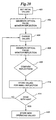
- FIG. 20 is a flow chart of a preferred embodiment of the feedback decision process of the present invention.
- FIG. 21 is a schematic block diagram of a preferred embodiment of the control electronics of the feedback control of the present invention.
- a 2x1 optical switch element has two input ports, but only one output port, and the light signal is selectively propagated either to or away from the one output port by activating the desired switch state.
- a 2x2 optical switch element there are two input ports, two wave guide channels, and a first output port and a second output port.
- the light signal in a 2x2 optical switch is selectively propagated primarily to the first output port by activating a first desired switch state and selectively propagated primarily to the second output port by activating a second desired switch state.
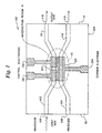
- a 2x2 optical switch element is a conventional 2x2 directional coupler 100, as shown for example in FIG. 1.
- an input side 101 has a pair of single mode wave guides 102 and 103, including wave guide sections 104 and 105 that carry light signals from input ports 106 and 108, respectively to an interaction region 110.
- an output side 111 has wave guide sections 112 and 114 that carry light signals to output ports 116 and 118, respectively from interaction region 110.
- a light signal entering coupler 100 at port 106 can be transferred within coupler 100 so as to exit from second wave guide 103 through wave guide section 114 at port 118 (in which case coupler 100 is in a "cross state"), or the light signal can be passed through coupler 100 so as to remain in first wave guide 102 through wave guide section 112 and exit at port 116 (in which case coupler 100 is in the "bar” state). Because light signals can be passed both ways through coupler 100, a light signal might also enter wave guide at port 116 and be transferred so as to exit second wave guide 103 at port 108 (the "cross” port), or be passed through so as to remain in first wave guide 102 and exit at port 106 (the "bar” port).
- each wave guide 102, 103 is arbitrarily divided into a number of sections for ease of explanation, although is will be understood that these sections are integrated together to operate as the light conduits of an optical switch element.
- wave guide channel sections 120 and 122 Located within interaction region 110 of coupler 100 are wave guide channel sections 120 and 122 which are coupled together by positioning at least a length (L) of channel sections 120 and 122 very close to one another with an effective separation (G).
- wave guide channel sections 120 and 122 are constructed so as not to restrict the light signal to staying within a particular wave guide channel. Consequently, a light signal passing through interaction region 110 will either stay within one wave guide channel, cross over to the other wave guide channel, or do both, depending upon the optical transmission properties of wave guide channel sections 120 and 122 within interaction region 110.
- the characteristic length required for a light signal to cross from one wave guide channel to the other is referred to as the effective coupling length (1).
- the electric field changes the optical transmission properties of wave guide channel sections 120 and 122. As a result, the way in which the light signal passes through interaction region 110 can also be changed.
- wave guide channel sections 120 and 122 are fabricated in an electro-optically active substrate 124 by increasing the refractive index of substrate 124 in the wave guides. Because wave guide channel sections 120 and 122 are physically close together in interaction region 110, the evanescent optical fields of the two channel sections 120 and 122 overlap, resulting in an optical coupling between wave guide channel sections 120 and 122.
- the effect of coupling between wave guide channel sections 120 and 122 can be selectively controlled by electro-optically modifying the refractive index in interaction region 110 via an electric field produced by control electrodes 130, 132 and 134 situated in interaction region 110 near wave guide channel sections 120 and 122.
- Two independent control electrodes (130 and 132) and a single common electrode (134) effectively create two electrode pairs that can electro-optically control the refractive index of interaction region 110.
- common electrode 134 can be implemented as two separate common electrodes.
- the use of two independent control electrodes in this manner is referred to as a directional coupler utilizing reverse differential propagation constant ( ⁇ ) control. Two control electrode pairs are used rather than a single electrode pair in order to obtain better control of the switch state of directional coupler 100.
- reverse differential propagation constant ( ⁇ ) control using two control electrodes reference is made to R.V. Schmidt and H. Kogelnik, "Electro-optically switched coupler with stepped ⁇ reversal using Ti-diffused LiNbO 3 wave guides", Applied Physics Letters, Vol. 28, No. 9, 1 May 1976, pp. 503-506.
- coupler 100 While it would be desirable if coupler 100 behaved exactly like a digital switch that was either always on (bar state) or always off (cross state), the control of the light signal as it passes through coupler 100 is not that simple. In practice, coupler 100 behaves more like a leaky two-way valve, with most of the light signal being transferred through the desired wave guide channel, but with some of the light signal leaking out the other wave guide channel. As long as the relative difference between the optical outputs of each wave guide channel is large enough, however, it is still possible to use coupler 100 as an effective optical switch having two operational states, the bar state and the cross state.
- a directional coupler 100 It is typical to define the operational state of a directional coupler 100 by the ratio of optical power exiting from the two optical ports 116 and 118 in response to a light signal incident upon optical port 106.
- the switching extinction ratio of directional coupler 100 By convention, the extinction ratio of a reverse ⁇ directional coupler is normally defined to be equal to 10log 10 ( c/b ), where b is the output power of the bar port and c is the output power of the cross port.
- the extinction ratio will be greater than some value dictated by the requirements of the system into which the optical switch element is incorporated.
- the value of the required extinction ratio might be 15 dB, meaning that less than about 1/30th of the light signal will be emerging from the non-intended port of directional coupler 100.
- V 1c and V 2c represents the operating voltages which should be applied to electrodes 130 and 132 in order to induce a particular directional coupler 100 to operate in the cross state.
- V 1b and V 2b which correspond to the operating voltages which should be applied to electrodes 130 and 132 in order to induce the same directional coupler 100 to operate in the bar state.
- X-branch optical switch element 140 is similar to directional coupler 100, except that a single control electrode pair 142 and 144 are used for electro-optical control, rather than two control electrode pairs 130, 132 and 134 in directional coupler 100. All of the remaining features of X-branch optical switch element 140 are similar to like-referenced elements of directional coupler 100. It will be seen, however, that the topology of wave guide channels 102, 104, 112 and 114 is somewhat simpler than in directional coupler 140. Within interaction region 110, wave guide channel sections 146 and 148 intersect one another, rather than the generally parallel configuration which is found for wave guide channel sections 122 and 124 of directional coupler 100.
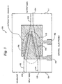
- Y-branch optical switch element 150 In Y-branch optical switch element 150, there are two wave guide channel sections 104 and 105 on input side 101; however, only a single wave guide channel section 152 and output port 154 on output side 111 are provided. Thus, unlike directional coupler 100 and X-branch optical switch element 140 which are 2x2 switch elements, Y-branch optical switch element is a 2x1 switch element. In a typical Y-branch optical switch element 150, interaction region 110 is primarily defined along the points where wave guide channel sections 156 and 158 converge together. Other elements of Y-branch optical switch element 150 are similar to similarly referenced elements in directional coupler 100.
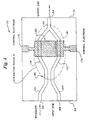
- balanced bridge optical switch element 170 is a 2x1 optical switch element having only a single output wave guide channel section 152 and output port 154.
- wave guide channel sections 172 and 174 have a topology which provides for a first interaction area 180 where wave guide channel sections 172 and 174 are positioned close to one another, but not within the influence of control electrodes 176 and 178, and a second interaction area 182 where wave guide channel sections 172 and 174 are positioned not as close to one another, but within the influence of control electrodes 176 and 178.
- the electrical field applied by control electrodes 176 and 178 electro-optically alters the propagation characteristics within second area 182 to control the relative optical phase of the optical signals which are split or combined.
- optical switch element 100 is a 2x2 optical switch element having two wave guide channels 102 and 103, with two wave guide channel sections 104, 105 and two ports 106, 108 on an input side 101 and two wave guide channel sections 112, 114 and two ports 116, 118 on an output side 111.
- Examples of such a 2x2 optical switch element are optical switch element 100 as shown in FIG. 1, optical switch element 140 as shown in FIG. 2, or any equivalent thereof.
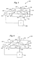
- An optical light source 202 introduces a light signal 204 into first input port 106 of optical switch element 100.
- Light signal 204 propagates through at least one wave guide channel section 206, 208 within interaction region 110 to either of output port 116 or 118 in response to an electrical field across interaction region 110.
- An optical reflector 210 causes a reflection 212 of at least a portion of light signal 204 to occur on output side 111 of optical switch element 100 that is propagated back through interaction region 110 to at least one wave guide channel section 104, 105, 206, 208.
- optical reflector 210 may be located in a variety of positions, so long as optical reflector 210 is at least beyond the side of interaction region 110 out of which light signal 204 passes.
- a photodetector 220 is operably coupled to a second input port 108 of optical switch element 100 to detect a portion 214 of reflection 212.
- Feedback control circuit 222 is operably coupled to photodetector 220 and optical switch element 100 for controlling at least one voltage applied to at least one pair of electrodes 224, 226 in response to portion 214 of reflection 212.
- Feedback control circuit 222 is arranged and operated so as to minimize portion 214 of reflection 212, thereby effectively tuning optical switch element 100 to a desired switch state. Where there is more than one desired switch state, feedback control circuit 222 has the ability to select among desired switch states.
- feedback control circuit 222 can tune optical switch element 100, it is necessary to understand how light passes through optical switch element 100 when optical switch element 100 is in different switch states.
- a first switch state for a 2x2 switch element in this example the "cross" or "normal” state, no voltage or a relatively small voltage is typically applied across electrodes 224 and 226.
- the propagation characteristics of wave guide channel sections 206, 208 would be designed such that light signal 204 would tend to cross from wave guide channel section 206 to wave guide channel section 208 while traversing through interaction region 110.
- a voltage is applied to electrodes 224 and 226 that electro-optically controls the propagation characteristics of properly designed wave guide channel sections 206 and 208 so that when light signal 204 propagates through interaction region 110 it travels straight through and light signal 204 tends to stay within wave guide channel section 206 and travel into wave guide channel 112.
- this second state it is intended that light signal 204 enters port 106, travels through channel sections 104, 206 and 112 and exits port 116, effectively taking a "straight" line through optical switch element 100.
- not all of light signal 204 will behave in the manner intended and the ideal is that the portion of light signal 204 exiting the output port, in this case port 116, should be as large as possible for this second switch state.
- switch element 100 Normally, if switch element 100 is to be tuned, for example, at a factory, to have an optimized extinction ratio for the first switch state, photodetectors would be connected to output ports 116 and 118 and the voltages applied to control electrodes 224 and 226 would be manually adjusted until the extinction ratio as measured between output ports 116 and 118 is maximized. As discussed in the background section of the application, this procedure can be accomplished only when switch element 100 is not being used as a switch and has, instead, been connected to measurement photodetectors to determine the switching extinction ratio of the device.
- optical reflector 210 is used to reflect a portion 212 of light signal 204 in wave guide channel section 114 back through interaction region 110.
- the majority of reflected portion 212 will remain in wave guide channel section 108 and a minor portion 214 of reflected portion 212 can then be detected by photodetector 220.
- the smaller the amount of light detected as portion 214 by photodetector 220 the smaller the amount of light that was reflected as reflected portion 212 by optical reflector 210; and, the smaller the amount of reflected portion 212 the smaller the amount of light signal 204 that is coming out of the non-intended output port 118 for this second switch state. Consequently, minimizing the reflected portion 214 by altering the voltages applied to control electrodes 224 and 226 under control of feedback control 220 optimizes the operational transfer characteristics of switch element 100 in the second switch state.
- the majority of light signal 204 now crosses over to wave guide channel sections 208 and 114. Again, a portion 212 is reflected and returns back through interaction region 110 which, because of the first switch state, will generally cross back over into wave guide channel sections 206 and 104, with only a small portion continuing on into wave guide channel section 105.
- system 200 for tuning of optical switch element 100 can be operated continually and is not confined to an "initial factory setting", for example.
- optical reflector 210 in an appropriate manner (e.g., a reflection of less than a few percent of the light signal)
- the transfer characteristic performance of optical switch element 200 is not significantly affected and is easily compensated for by the ability to of system 200 to continually operate switch element 100 at an optimum extinction ratio.
- it is relatively straight-forward for system 200 to perform continuous feedback control over the performance characteristics of optical switch element 100 so as to compensate for changes in operating conditions, input light signal conditions, voltage drift and the like.
- Another advantage of the present invention is that it allows for tuning of an optical switch element without the need for or additional cost and complexity associated with adding optical splitters or detectors to monitor the transfer characteristics of the switch 100 from output side 111.
- the present invention can also make use of existing detectors and detection circuitry to accomplish the functions of detector 220 of the present invention.
- optical switch element 150 is a 2x1 optical switch element having two wave guide channel sections 102, 103 and two ports 106, 108 on an input side 101 and one wave guide channel section 152 and one port 156 on an output side 111.
- Examples of such a 2x1 optical switch element are optical switch element 150 as shown in FIG. 3, optical switch element 170 as shown in FIG. 4, or any equivalent thereof.
- An optical light source 202 introduces a light signal 204 into first input port 106 of optical switch element 150.
- Light signal 204 selectively propagates through at least one wave guide channel sections 206, 208 within interaction region 110 to output port 156 in response to an electrical field across interaction region 110.
- An optical reflector 210 causes a reflection 212 of at least a portion of light signal 204 to occur on output side 111 of optical switch element 200 that is propagated back through interaction region 110 to at least one wave guide channel sections 104, 105, 206, 208.
- optical reflector 210 may be located in a variety of positions, so long as optical reflector 210 is at least beyond the side of interaction region 110 out of which light signal 204 passes.
- a photodetector 220 is operably coupled to a second input port 108 of optical switch element 150 to detect a portion 214 of reflection 212.
- Feedback control circuit 222 is operably coupled to photodetector 220 and optical switch element 150 for controlling at least one voltage applied to at least one pair of electrodes 224, 226 in response to portion 214 of reflection 212.
- Feedback control circuit 222 is arranged and operated so as to minimize portion 214 of reflection 212, thereby effectively tuning optical switch element 150 to a desired switch state.
- the first and second switch states of a 2x1 optical switch element 150 are generally referred to as “on” and “off” in reference, for example, to a first one of input ports 106, 108.
- the "on" state will be defined as the switch state providing the lowest loss for light propagating from port 106 to port 156 (or from port 156 to port 106). This state is also the state of highest loss for light propagating from port 156 to port 108 (or port 108 to port 156).
- the "off' state will be defined as the state having the lowcost loss for light propagation from port 108 to port 156 (or port 156 to port 108), and the highest loss for light propagating from port 106 to port 156 (or port 156 to port 106).
- the timing of the switch 150 to the optimum "on” state then proceeds as follows.
- light signal 204 launched into port 106 from 202 propagates with low loss through intersection region 110 into wave guide section 152.
- a portion 212 of light signal 204 is reflected by optical reflector 210 back through wave guide portion 152 into interaction region 110.
- the switch is in the on state, the majority of the reflected signal 212 is directed into wave guide section 102, having only a small amount of light in wave guide section 104, so that a minimum signal is detected by detector 220.
- the smaller the light detected at 220 the better the timing of the "on” state. Therefore, minimizing the signal detected at 220 optimizes the transfer characteristic of the switch in the "on” state.
- the timing of the switch 150 to the optimum "off' state proceeds similarly.
- light signal 204 entering port 106 experiences high loss in interaction region 110; the higher the loss the better the "off” state.
- a small portion 212 of the light signal looking through the intersection region 110 will be reflected by reflector 210 back into interaction region 110.
- This small signal will be detected, in the off state, with the low loss into wave guide section 104 and out port 108 to detector 220.
- the amount of light available to be reflected at reflector 210 is limited by the high loss of the path between ports 106 and 156 in the off state, minimizing the signal exiting port 108 and detected by detector 220 optimizes the transfer characteristic of the switch in the "off" state.
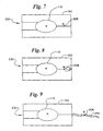
- FIGs. 7, 8 and 9 are plan views of three different embodiments of integrated optical switch element 150 in which optical reflector 210 is positioned in various positions with respect to interaction region 110.
- optical reflector 210 is positioned within wave guide channel section 152 on the substrate of electro-optic material which comprises optical switch element 150.
- optical reflector 210 can be implemented by a variety of means, including, geometric, structural or chemical alterations of wave guide channel section 152 or the cladding layer surrounding wave guide channel section 152, such as by etching to create an interference grating, doping of the electro-optic material within wave guide channel section 152 so as to alter the optical propagation characteristics to generate the desired reflected signal 212, electro-optically altering the propagation characteristics of wave guide channel section 152 by use of a further set of electrodes positioned beyond interaction region 110, by interaction with an acoustic wave or via photo-induced refractive index changes.
- optical reflector 210 is located at output port 156 at the boundary of optical switch element 150.
- this embodiment would take advantage of a slight mismatch in the boundary condition at output port 156 that results in a small reflection occurring at the boundary interface. For example, if there were a slight mismatch in between the optical index of wave guide channel section 152 and an optical transmission path connected to port 156, this mismatch of the index refraction can generate the desired reflected signal 212. Alternatively, reflected signal 212 could also be generated as a result of a reflective coating being applied to the chip facet of output port 156.
- Still other versions of this embodiment would include a temporary or set-up tuning version where a complete reflector, such as a mirror or the like, or even a partial reflector, is directly coupled to output port 156 for purposes of initially tuning or setting up the optimum transfer characteristics of optical switch element 150.
- a complete reflector such as a mirror or the like, or even a partial reflector
- optical reflector 210 is positioned external to optical switch element 150.
- control system 230 takes advantage of any number of reflections which may occur within an optical network that are external to optical switch element 150.
- optical reflector 210 may be an imperfection in regularity within an optical fiber 240 that is optically coupled to output port 156.
- optical reflector 210 may be any of the optical interface mismatch situations which have been previously described which can generate a reflected signal 212. It will be apparent to a person skilled in the art that there are numerous mechanisms and techniques by which an effective optical reflector 210 can be either temporarily or permanently created as part of an optical network to provide necessary reflected signal 212 for purposes of the present invention.
- optical reflector 210 be sufficient to generate a reflected signal 212 that can be measured by the sensitivities of photodetector 220 when optical switch element 100, 150 is operating in an optimum mode with high extinction.
- reflected signal 212 would comprise between 1% and 50% of optical signal 204 within wave guide channel 156, for example. With reflected signal 212 operating in these ranges, the reflected portion 214 which will reach photodetector 220 for an optical switch element having a switching restriction ratio of 30db, for example, would be between 0.001% and 0.05%, ignoring losses.
- reflected signal 212 be between about 0.1% and 10%, and ideally about 4%, so that the portion of light signal 204 consumed by reflected signal 212 is significant enough to be detected, but not so large as to detract from the effective operation of the switch element. While the relationship between reflected signal 214 and light signal 204 is preferably linear, so as to simplify the control system of feedback control circuit 222, it will be understood that this relationship could also be non-linear as long as the relationship is generally stable and known to feedback control circuit 222.
- tuning system 230 in accordance with the present invention is shown having photodetector 220 located in various positions with respect to optical switch element 150.
- photodetector 220 is positioned on the same electro-optic substrate 124 as interaction region 110 of optical switch element 150.
- photodetector 222 could be integrated into wave guide channel 104. Examples of how it would be possible to accomplish this are shown, for example, in U.S. Patents Nos. 5,065,201 and 5,261,014.
- photodetector 222 is located on a substrate 242 that is separate from, and adjacent to, electro-optic substrate 124 on which optical switch element 150 is located.
- This multi-chip module embodiment can be utilized to achieve the advantages of the embodiment shown in FIG. 10, but to simplify the manufacturing and assembly techniques of tuning system 230.
- photodetector 220 is located physically removed from optical switch element 150 and is optically connected to second input port 108 by an optical fiber 244, for example.
- Optical switch matrix 300 will include at least two optical switch elements 310, 320 which have output ports and input ports that are interconnected to form a switching matrix. As a minimum condition for such a optical switching matrix, at least one output port of matrix element 310 would be connected to an input port of matrix element 320. Examples of switching matrixes of this type are known in Thylen, L. and Granestand, P., "Switch Arrays for Photonic Switching: Status Review and Prospects", IEEE Globecom '90 Conf. Proc., Vol. 2, Dec. 1990, pp.
- optical switch matrixes 300 to which control system 250 of the present invention can be applied can be constructed in a number of alternate embodiments such as within a common substrate, or in a multiple substrate, multiple-chip module arrangement, or even as individual discreet matrix elements 310, 320 which are optically connected together by optical fiber or other wave guide channels.
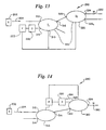
- light signal 204 is generated by an optical source 202 and is directed into an input port 312 of matrix element 310.
- Output port 316 is optically connected to input port 322 of matrix element 320 having an optical reflector 252 located beyond an output side of an interaction region of this matrix element.
- optical reflector 252 is located external to matrix element 320, although any of the positional embodiments of the optical reflector described with respect to Figures 10, 11 and 12 could be utilized for tuning system 250. A number of different feedback control arrangements can be accomplished through this embodiment.
- matrix element 320 is controlled so as to be in an ideal state in which light signal 204 is propagated to output port 324, then the reflected signal caused by optical reflector 252 will essentially mimic the reflected signal that would be caused by reflection external to port 316 and feedback control circuit 222 can use this information to tune matrix element 310 in isolation.
- the signal reflected by optical reflector 252 can be used to optimize the transfer characteristics of the combined switch matrix elements 310 and 320. In this case, feedback control circuit 222 would be simultaneously controlling the voltage electrodes for both matrix element 310 and 320.
- matrix element 310 had previously been optimized and matrix element 320 is the focus of optimization feedback control circuit 222.
- the optimized control voltages would be applied to matrix element 310 and the control voltages would be altered on matrix element 320 so as to still minimize the reflected signal measured at detector 220.
- optical reflector 252 can comprise more than a single reflection mechanism which operates to provide a reflected signal 254 that is detected by photodetector 220. Even though multiple reflection points may be associated with the reflected signal 254, the fundamental premise that reflected signal 254 is to be minimized by tuning system 250 does not change. In the case of switch matrix 300, the objective would be to exercise all of the possible switch combinations presented by switch matrix 300 and, for each such combination, minimize the combined reflected signal 254 which is detected by photodetector 220.
- a photodetector 220 would need to be coupled to an output port 314 of each matrix element 310. This could be accomplished either by providing separate photodetectors 220 for each matrix element 310, or by providing a single photodetector 220 and appropriate optical switching devices under control of feedback control circuit 222 to direct reflected signal 254 from the matrix element 310 under test into photodetector 220.
- photodetector 220 is now connected to an input port 328 of matrix element 320.
- the embodiment of tuning system 260 as shown in FIG. 14 uses the forward transfer characteristics of matrix element 310 and the reverse transfer characteristics of 310 and the reverse transfer characteristics of matrix element 320 to accomplish feedback optimization.
- a transfer characteristics of matrix element 310 can be optimized by maximizing or minimizing the amount of light signal 204 exiting from output port 306 which now becomes the input light signal for input port 322 of matrix element 320.
- Matrix element 320 is optimized by measuring the reverse transfer characteristics associated with reflected signal 264 at detector 220.
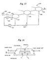
- FIG. 15 shows another embodiment of tuning system 270 having a optical matrix 300 which is at least three switches deep.
- one or more matrix elements 330 are disposed between the matrix element 310 into which light signal 204 is launched and matrix element 320 beyond which optical reflector 272 is positioned.
- the objective of tuning system 270 is to minimize the reflected signal 274 detected at photodetector 220. It would be appreciated, that either of the embodiments of the positions of photodetector 220 as shown in FIG. 13 and FIG. 14 could be implemented in tuning system 270.
- matrix elements 310 and 330 could be reversed such that light signal 204 from light source 202 was introduced into the "middle" of switch matrix 300.
- detector 220 would need to be positioned at an input port of matrix element 330 in order to include matrix element 330 within the scope of the matrix elements that could be tuned by tuning system 270.
- the effective depth of matrix elements 310, 320 and 330 which can be tuned by a tuning system 270 will primarily be a function of the number and magnitude of inherent reflections within matrix 300 which can be detected by tuning system 270, and by the sensitivity of photodetector 220 to accurately measure and differentiate between very small variations in reflected signal 274.
- optical switch elements can improve the performance of an OTDR system by selectively protecting the high gain optical detection system used by the OTDR system from excessively strong reflections that would otherwise saturate the detector system and produce a "dead zone" in which no reflections from other fiber features or flaws can be seen by the OTDR.
- Examples of OTDRs and the use of optical switch elements in an OTDR are shown in U.S. Patents Nos. 5,149,961; 5,144,125; 5,093,568; 5,072,111; 5,045,689; 5,028,775; 5,023,445; 5,013,907; 4,968,880; and 4,960,989.
- FIG. 16 Typical configuration of an integrated optical switch in an OTDR is shown in FIG. 16.
- a fiber under test 300 is optically coupled to one output port 116, 118 of a pigtailed LiNbO 3 directional coupler 100.
- a laser diode 222 and a detector 220 are connected to the input ports 112 and 114, respectively.
- the voltages V 1 and V 2 applied to control electrodes 130 and 132 are varied under control of feedback control circuit 222 to put the switch in an optimal cross or bar state.
- the bar state is used to launch light into the fiber; the cross state allows reflections from features in the fiber to reach the detector for analysis.
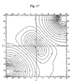
- the transfer function is a two-dimensional map of the operational states of the directional coupler for all possible combinations of operating voltages V 1 and V 2 . It will be understood that for different electrode configurations of the directional coupler (e.g., one pair of electrodes or three or more pairs of electrodes) the set of operating voltages for the cross states and bar states of the device will include a number of voltage values corresponding to the number of electrode pair combinations.
- the extinction ratio is measured for representative values of operating voltages V 1 and V 2 , and the results are plotted as equal-value contours on a contour plot as shown, for example, in FIG. 17 for a TE polarized light signal as measured with respect to the switch element shown in FIG. 16.
- a positive contour i.e., a ratio greater than 1
- a negative contour i.e., a ratio less than 1
- Areas of the contour plots which represent high-quality cross states can be seen as peaks or ridges and areas of the contour plot which represent high-quality bar states can be seen as valleys.
- the required extinction ratio for high quality cross states will be at least 15 dB, although it will be understood that different values for the extinction ratio necessary to achieve a high quality cross state may be required for different applications or uses of a directional coupler 100.
- the measured extinction ratios of directional coupler 100 are not optimized for use with the present invention because no precautions were taken to prevent reflections from the fiber-to-chip interface at output ports 116 and 118.
- coherent light is used for light signal 204, significant reflections from both output ports 116 and 118 are experienced and oscillations in the apparent extinction ratio as measured can results to due to interferometric effects.
- FIG. 18 compares the calculated reflected power, based on Eq. (2) and the measured switch extinction ratio from FIG. 17 for directional coupler 100 of FIG. 16. In this case, it has been assumed that the reflection at each fiber-to-chip interface at output port 116 and 118 is 3.6%, and the input power of P o is -10dB. Fiber coupling loss and interferometric effects have been neglected.
- a controlled reflection for tuning could be provided for the OTDR system shown in FIG. 16, for example, by leaving output port 118 open to the air (14% reflection), or by attaching a dead-end length of fiber to port 118 (4% reflection), or by coating output port 118 for additional reflection, or simply be leaving the connector between output port 116 and fiber under test 300 disconnected during the tuning process (about 4% reflection).
- Still another technique for accomplishing polarization-independence would be to use a polarization-maintaining (PM) fiber between light source 202 and switch element 100 with light signal 204 at 45 degrees to the PM fiber birefringence axis and the PM fiber aligned with its birefringence axis along a principal axis of switch element 100, or by light signal 204 being launched along the axis of PM fiber and the fiber axis being aligned at 45 degrees with respect to the principal axis of switch element 100.
- Other alternatives would be to use some type of polarizing (PZ) fiber with a fiber polarization axis aligned with the polarization of light signal 204, but at 45 degrees to the axes of switch element 100.
- step 400 initial values of (V 1 , V 2 ) approximating the cross state are established, either from the last known optimized cross state values, or from best estimated values based on the design of the directional coupler 100 being tuned.
- step 402 an optical pulse light signal 204 (or series of pulses) is launched from light source 202 and the optical power of P b is monitored at detector 220.
- Feedback control circuit 222 then adjusts the values of voltages (V 1 , V 2 ) by a predetermined increment at step 404.
- Another optical pulse light signal 204 (or series of pulses) is launched at step 406 and the reflected optical power is monitored at detector 220.
- Step 408 compares the two detected values from steps 402 and 406 and step 412 stores the voltage values (V 1 , V 2 ) corresponding to the smaller monitored optical power P b as the new initial values.
- control is returned to step 402 until the predetermined incremental hunt pattern has been exhausted and/or the minimum has been found or the new determined tuned cross state operating values for voltages (V 1 , V 2 ) are stored and the feedback routine is exited at step 416.
- the same routine can be used, starting with approximate bar state voltages, to optimize the bar state operating voltages.
- FIG. 21 A block diagram of a feedback control circuit 222 for use with the present invention is shown in FIG. 21.
- Control voltages for each of the three control electrodes 130, 132 and 134 of directional coupler 100 are provided by three digital-to-analog converters 410, each coupled to driver amps 412.
- Up/down counters 418 are used to hold the six voltage levels corresponding to the ON and OFF levels of the three control electrode 130, 132 and 134.
- the desired state of the switch for tuning purposes is provided as an input to a microprocessor 420, in this case through an A/D 422 and UART 424.
- UART 424 also toggles buffers 416 between the ON and OFF states.
- Microprocessor 420 keeps track of the light levels detected by photodetector 220 and changes the voltage levels stored in up/down counters 418 by small, fixed amounts, corresponding to steps of approximately 0.2 V in each of eight symmetrical directions, separated by 45 degrees (in the two-dimensional voltage space of FIG. 19), around the currently stored "best operating point". Whenever a decrease in the detected output power is found, the new voltage levels are stored in the up/down counters.
Landscapes
- Physics & Mathematics (AREA)
- Nonlinear Science (AREA)
- General Physics & Mathematics (AREA)
- Optics & Photonics (AREA)
- Optical Integrated Circuits (AREA)
- Optical Modulation, Optical Deflection, Nonlinear Optics, Optical Demodulation, Optical Logic Elements (AREA)
Claims (14)
- System zum Abstimmen mindestens eines integrierten optischen Schaltelements (100), wobei jedes optische Schaltelement aus einem elektrooptischen Material gebildet ist, das aufweist: einen Interaktionsbereich (110) und mindestens einen durch den Interaktionsbereich (110) verlaufenden Wellenleiterkanal (206,208), mindestens einen ersten Eingangs-Port (106) und einen zweiten Eingangs-Port (108), die an einer ersten Seite des Interaktionsbereichs definiert sind, in die ein Lichtsignal eintritt, mindestens einen Ausgangs-Port (116,118), der an einer zweiten Seite des Interaktionsbereichs definiert ist, aus der das Lichtsignal selektiv austritt, und mindestens ein Paar von Elektroden (224,226), um über dem Interaktionsbereich selektiv ein elektrisches Feld zu erzeugen, das einen gewünschten Schaltzustand des optischen Schaltelements elektrooptisch erzeugt, wobei das System aufweist:dadurch gekennzeichnet, dass das System ferner aufweist:eine optische Lichtquelle (202) zum Einleiten eines Lichtsignals (204) in einen ersten Eingangs-Port (106) eines optischen Schaltelements (100), wobei sich auf ein elektrisches Feld an dem Interaktionsbereich (110) hin das Lichtsignal durch mindestens einen Wellenleiterkanal (206,208) zu einem Ausgangs-Port (116,118) ausbreitet,eine Einrichtung (210) zum Verursachen des Auftretens einer Reflexion (212) mindestens eines Teils des Lichtsignals hinter einer zweiten Seite des Interaktionsbereichs (110), wobei die Reflexion durch mindestens einen Wellenleiterkanal (104,105,206,208) zurückgeleitet wird,einen Lichtdetektor (220), der zur Verbindung mit dem zweiten Eingangs-Port (108) des integrierten optischen Schaltelements (100) angeordnet ist, um einen Teil (214) der Reflexion (212) zu detektieren, undeine betriebsmäßig mit dem Lichtdetektor (220) und mindestens einem optischen Schaltelement (100) verbundenen Rückkopplungseinrichtung (222) zum Steuern mindestens einer an das mindestens eine Paar von Elektroden (224,226) angelegten Spannung auf den von dem Lichtdetektor (220) detektierten Teil (214) der Reflexion (212) hin, um den Teil (214) der Reflexion (212) zu minimieren und dadurch selektiv mindestens eines der integrierten optischen Schaltelemente (100) auf einen gewünschten Schaltzustand abzustimmen.
- System nach Anspruch 1, bei dem mindestens eines der integrierten optischen Schaltelemente nur einen Ausgangs-Port (152) aufweist und bei dem durch Aktivieren des gewünschten Schaltzustands das Lichtsignal selektiv aus dem Ausgangs-Port austritt und durch Aktivieren des gewünschten zweiten Schaltzustands selektiv aus dem einen Ausgangs-Port ausgeschlossen wird.
- System nach Anspruch 1, bei dem mindestens eines der integrierten optischen Schaltelemente zwei sich durch den Interaktionsbereich (110) erstreckende Wellenleiterkanäle (120,122) aufweist, wobei sich ein erster Wellenleiterkanal zwischen dem ersten Eingangs-Port (106) und dem ersten Ausgangs-Port (116) erstreckt, und sich ein zweiter Wellenleiterkanal zwischen dem zweiten Eingangs-Port (108) und dem zweiten Ausgangs-Port (118) erstreckt, und bei dem das Lichtsignal selektiv durch Aktivieren eines ersten gewünschten Schaltzustands primär aus dem ersten Ausgangs-Port (116) austritt und selektiv durch Aktivieren eines zweiten gewünschten Schaltzustands primär aus dem zweiten Ausgangs-Port (118) austritt.
- System nach Anspruch 1, bei dem das integrierte optische Schaltelement aus der Gruppe gewählt ist, die einen Y-Abzweig-Schalter (150), einen Schalter (170) mit abgeglichener Brücke, einen X-Abzweig-Schalter (140) oder einen Richtkoppler (100) aufweist.
- System nach Anspruch 1, bei dem die zum Verursachen einer Reflexion (212) vorgesehene Einrichtung (210) an einer Position angeordnet ist, die aus der Gruppe gewählt ist, welche eine Position innerhalb eines optischen Schaltelements, eine Position an einem Grenzbereich eines optischen Schaltelements oder eine Position außerhalb mindestens eines optischen Schaltelements aufweist.
- System nach Anspruch 1, bei dem die Position des Lichtdetektors (220) aus der Gruppe gewählt ist, die aufweist: eine Position auf einem mit dem zweiten Eingangs-Port des integrierten optischen Schaltelements (100) gemeinsamen Substrat, das mit dem zweiten Eingangs-Port (108) des integrierten optischen Schaltelements (100) optisch verbunden ist; eine Position auf einem Substrat, das von einem Substrat getrennt ist, auf der der zweite Eingangs-Port (108) des integrierten optischen Schaltelements (100) angeordnet ist, wobei das Substrat des Lichtdetektors (220) und das Substrat des integrierten optischen Schaltelements (100) beide Teil eines Mehrfachchipmoduls sind, bei dem der Lichtdetektor (220) mit dem zweiten Eingangs-Port (108) des integrierten optischen Schaltelements (100) optisch verbunden ist; und einer Position, die physisch von einem integrierten optischen Schaltelements getrennt ist, das den zweiten Eingangs-Port (108) aufweist, der über eine Optikfaser (224) oder ein anderes optisches Element mit dem Lichtdetektor (220) optisch verbunden ist.
- System nach Anspruch 1, bei dem der Interaktionsbereich jedes optischen Schaltelements definiert ist durch den größeren von (a) einem Bereich, der entlang mindestens eines Wellenleiterkanals definiert ist, in dem Modifikationen optischer Eigenschaften mindestens eines Wellenleiterkanals zwecks Steuern von Lichtsignalen in mindestens einem Wellenleiterkanal existieren, und b) einem Bereich, in dem das elektrische Feld zwecks Steuern von Lichtsignalen in mindestens einem Wellenleiterkanal aufgebracht wird.
- System nach Anspruch 1, bei dem das Lichtsignal in einen ersten Eingangs-Port (106) eines ersten integrierten optischen Schaltelements eintritt und die Reflexion hinter einer zweiten Seite eines Interaktionsbereiches eines zweiten optischen Schaltelements auftritt, die mit dem ersten optischen Schaltelement optisch verbunden ist.
- System nach Anspruch 1, bei dem das Lichtsignal in einen ersten Eingangs-Port (312) eines ersten integrierten optischen Schaltelements (310) eintritt und der Teil der Reflexion an einem zweiten Eingangs-Port eines zweiten integrierten optischen Schaltelements (320) detektiert wird, der mit dem ersten optischen Schaltelement optisch verbunden ist.
- System nach Anspruch 9, bei dem die Reflexion hinter einer zweiten Seite eines Interaktionsbereichs eines dritten integrierten optischen Schaltelements (330) auftritt.
- System nach Anspruch 10, bei dem die Rückkopplungseinrichtung mindestens ein Schaltelement durch Anlegen der Spannungen an mindestens ein Paar von Elektroden steuert, die aus der Gruppe gewählt sind, welche mindestens ein Paar von Elektroden des ersten integrierten optischen Schaltelements (310); mindestens ein Paar von Elektroden des zweiten integrierten optischen Schaltelements (320); mindestens ein Paar von Elektroden des dritten integrierten optischen Schaltelements (330); oder eine beliebige Kombination derselben aufweist.
- System nach Anspruch 1, bei dem mehrere optische Schaltelemente vorgesehen sind und bei dem mehrere Lichtdetektoren vorgesehen sind, von denen jeder mit einem zweiten Eingangs-Port eines bestimmten der mehreren optischen Schaltelemente optisch verbunden ist, und bei dem die Rückkopplungseinrichtung die von den mehreren Lichtdetektoren detektierten Reflexionen selektiv verwendet.
- System nach Anspruch 1, bei dem mindestens ein optisches Schaltelement Teil eines optischen Zeitdomänen-Reflektometers (OTDR) ist, und bei dem die optische Lichtquelle eine Laserlichtquelle in dem OTDR ist, der Lichtdetektor ein Lichtdetektor in einem optischen Detektionssystem des OTDR ist, und die Rückkopplungseinrichtung ein Software-Programm aufweist, das in einem Computer-Prozessor in dem OTDR ausgeführt wird und mindestens eine Schaltungseinrichtung zum Einstellen der dem mindestens einen Elektrodenpaar des optischen Schaltelements zugeführten Spannungen steuert.
- Verfahren zum Abstimmen mindestens eines integrierten optischen Schaltelements (100), wobei jedes optische Schaltelement aus einem elektrooptischen Material gebildet ist, das aufweist: einen Interaktionsbereich (110) und mindestens einen durch den Interaktionsbereich (110) verlaufenden Wellenleiterkanal (206,208), mindestens einen ersten Eingangs-Port (106) und einen zweiten Eingangs-Port (108), die an einer ersten Seite des Interaktionsbereichs definiert sind, in die ein Lichtsignal eintritt, mindestens einen Ausgangs-Port (116,118), der an einer zweiten Seite des Interaktionsbereichs definiert ist, aus der das Lichtsignal selektiv austritt, und mindestens ein Paar von Elektroden (224,226), um an dem Interaktionsbereich selektiv ein elektrischen Feld zu erzeugen, das einen gewünschten Schaltzustand des optischen Schaltelements elektrooptisch erzeugt, mit den folgenden Schritten:wobei das Verfahren durch die folgenden Schritte gekennzeichnet ist:(a) Einleiten eines Lichtsignals (204) in den ersten Eingangs-Port (106), wobei sich auf ein elektrisches Feld an dem Interaktionsbereich (110) hin das Lichtsignal durch den mindestens einen Wellenleiterkanal (206,208) zu dem Ausgangs-Port (116,118) ausbreitet,(b) Verursachen des Auftretens einer Reflexion (212) mindestens eines Teils des Lichtsignals hinter einer zweiten Seite des Interaktionsbereichs (110), wobei die Reflexion durch mindestens einen Wellenleiterkanal (104,105,206,208) zurückgeleitet wird,(c) Detektieren eines Teils (214) der Reflexion (212) von Schritt (b) an dem zweiten Eingangs-Port (108); und(d) Steuern einer oder mehrerer an das mindestens einen Paar von Elektroden (224,226) angelegter Spannungen auf den in Schritt (c) detektierten Teil (214) der Reflexion (212) hin, um den Teil (214) der in Schritt (c) detektierten Reflexion zu minimieren und dadurch selektiv mindestens ein optisches Schaltelement (100) auf den gewünschten Schaltzustand abzustimmen.
Applications Claiming Priority (3)
| Application Number | Priority Date | Filing Date | Title |
|---|---|---|---|
| US08/408,214 US5566263A (en) | 1995-03-22 | 1995-03-22 | System for tuning an integrated optical switch element |
| US408214 | 1995-03-22 | ||
| PCT/US1996/002084 WO1996029625A1 (en) | 1995-03-22 | 1996-02-14 | System for tuning an integrated optical switch element |
Publications (2)
| Publication Number | Publication Date |
|---|---|
| EP0815487A1 EP0815487A1 (de) | 1998-01-07 |
| EP0815487B1 true EP0815487B1 (de) | 2001-11-28 |
Family
ID=23615327
Family Applications (1)
| Application Number | Title | Priority Date | Filing Date |
|---|---|---|---|
| EP96906468A Expired - Lifetime EP0815487B1 (de) | 1995-03-22 | 1996-02-14 | Anordnung zur abstimmung eines integrierten optischen schaltelementes |
Country Status (5)
| Country | Link |
|---|---|
| US (1) | US5566263A (de) |
| EP (1) | EP0815487B1 (de) |
| JP (1) | JPH11502319A (de) |
| DE (1) | DE69617407T2 (de) |
| WO (1) | WO1996029625A1 (de) |
Families Citing this family (20)
| Publication number | Priority date | Publication date | Assignee | Title |
|---|---|---|---|---|
| SE513864C2 (sv) * | 1995-09-01 | 2000-11-20 | Ericsson Telefon Ab L M | Logikkretsar innefattande Y-grenelektronvågomkopplare |
| JPH10293158A (ja) * | 1997-04-18 | 1998-11-04 | Advantest Corp | Ic試験装置 |
| JP3257510B2 (ja) * | 1998-05-29 | 2002-02-18 | 日本電気株式会社 | 光デバイス |
| US6154586A (en) * | 1998-12-24 | 2000-11-28 | Jds Fitel Inc. | Optical switch mechanism |
| US6393185B1 (en) * | 1999-11-03 | 2002-05-21 | Sparkolor Corporation | Differential waveguide pair |
| WO2002037622A2 (en) | 2000-11-06 | 2002-05-10 | Vitesse Semiconductor Corporation | Method of controlling the turn off characteristics of a vcsel diode |
| US6470104B2 (en) * | 2000-12-12 | 2002-10-22 | Intel Corporation | Method and apparatus for switching an optical beam by modulating the phase of a portion of the optical beam in a semiconductor substrate |
| US6760493B2 (en) * | 2001-06-28 | 2004-07-06 | Avanex Corporation | Coplanar integrated optical waveguide electro-optical modulator |
| JP4676099B2 (ja) * | 2001-08-06 | 2011-04-27 | 株式会社日立製作所 | 反射モニタ機能を備え反射検出可能な光切替装置、及び反射測定システム |
| US20030138209A1 (en) * | 2002-01-10 | 2003-07-24 | Chan Edward Keat Leam | Filter device using thermo-optically controlled bragg grating |
| US6785430B2 (en) | 2002-02-25 | 2004-08-31 | Intel Corporation | Method and apparatus for integrating an optical transmit module |
| US6775425B2 (en) * | 2002-06-26 | 2004-08-10 | Intel Corporation | Method and apparatus for adjusting the phase of an optical beam |
| US20060078258A1 (en) * | 2004-10-07 | 2006-04-13 | University Of Toledo | Apparatus and method for trimming and tuning coupled photonic waveguides |
| US20060228121A1 (en) * | 2005-03-29 | 2006-10-12 | General Electric Company | Remote monitoring system and method |
| US7400788B2 (en) * | 2005-07-15 | 2008-07-15 | The United States Of America As Represented By The Secretary Of Air Force | Linearized optical modulator having a plurality of coupling functions |
| CA2584084A1 (en) * | 2006-04-05 | 2007-10-05 | Mojgan Daneshmand | Multi-port monolithic rf mems switches and switch matrices |
| US9684131B2 (en) * | 2014-04-04 | 2017-06-20 | Huawei Technologies., Ltd. | Apparatus and method for an optical switch having a 2×1 multi-mode interferometer and photodetector |
| US9941957B2 (en) | 2016-01-07 | 2018-04-10 | Luxtera, Inc. | Method and system for connectionless integrated optical receiver and transmitter test |
| EP3312582B1 (de) * | 2016-10-20 | 2020-02-26 | Xieon Networks S.à r.l. | Otdr mit elektroabsorptionsmodulator zur impulsformung und impulsdetektion |
| CN114545564B (zh) * | 2020-11-24 | 2023-04-14 | 青岛海信宽带多媒体技术有限公司 | 一种光模块 |
Family Cites Families (25)
| Publication number | Priority date | Publication date | Assignee | Title |
|---|---|---|---|---|
| JPS60147716A (ja) * | 1984-01-11 | 1985-08-03 | Nec Corp | 消光比制御光送信装置 |
| US4769534A (en) * | 1986-11-17 | 1988-09-06 | Tektronix, Inc. | Optical detector with storage effects reduction |
| GB2214023B (en) * | 1987-12-17 | 1992-03-25 | Plessey Co Plc | Control system for integrated optical devices |
| US5218468A (en) * | 1988-05-18 | 1993-06-08 | British Telecommunications Public Limited Company | Electro-optic device |
| GB8811689D0 (en) * | 1988-05-18 | 1988-06-22 | British Telecomm | Electro-optic device |
| JPH0224635A (ja) * | 1988-07-14 | 1990-01-26 | Fujitsu Ltd | 光スイッチ制御方式 |
| FR2640379B1 (fr) * | 1988-12-14 | 1994-07-01 | Centre Nat Rech Scient | Procede d'analyse de composants d'optique guidee, fibres optiques ou reseaux de guides optiques par reflectometrie temporelle et reflectometre dans le domaine temporel |
| DE68907886T2 (de) * | 1989-01-24 | 1994-01-13 | Hewlett Packard Gmbh | Verfahren und Vorrichtung zum Anwenden von optischen Zeitbereichsreflektometern. |
| JPH0748553B2 (ja) * | 1989-03-14 | 1995-05-24 | シャープ株式会社 | 半導体装置 |
| US4960989A (en) * | 1989-03-28 | 1990-10-02 | Photon Kinetics Inc. | Optical time domain reflectometer having a receiver with selectively controlled gain |
| US5028775A (en) * | 1989-06-30 | 1991-07-02 | Anritsu Corporation | Optical time domain reflectometer using optical element with three control modes of oscillation, attenuation and amplification |
| CA2021572C (en) * | 1989-07-20 | 1994-08-16 | Hisao Kawashima | Optical control device |
| US5020872A (en) * | 1990-01-04 | 1991-06-04 | Smiths Industries Aerospace & Defense Systems Incorporated | Method of operating an electrooptic modulator |
| JPH03257423A (ja) * | 1990-03-08 | 1991-11-15 | Fujitsu Ltd | 導波路型光変調器の動作点トリミング方法 |
| US5013907A (en) * | 1990-03-27 | 1991-05-07 | Tektronix, Inc. | Optical time domain testing instrument |
| US5023445A (en) * | 1990-04-27 | 1991-06-11 | Tektronix, Inc. | Signal acquisition method and automatic masking system for an OTDR |
| US5149961A (en) * | 1990-05-15 | 1992-09-22 | Eg&G, Ltd. | Method and apparatus for optical fiber length determination |
| US5072111A (en) * | 1990-09-04 | 1991-12-10 | The United States Of America As Represented By The Secretary Of The Army | Optical time domain reflectometer calibration system |
| US5144125A (en) * | 1990-12-12 | 1992-09-01 | The Babcock & Wilcox Company | Fiber optic based fire detection and tracking system |
| US5093568A (en) * | 1990-12-14 | 1992-03-03 | John Maycock | Monitoring system for fiber optic cables utilizing an OTDR for detection of signal loss and automatic location of faults in the cable |
| JPH0534650A (ja) * | 1991-05-10 | 1993-02-12 | Fujitsu Ltd | モニタ付分岐干渉型光変調器 |
| US5255334A (en) * | 1991-06-03 | 1993-10-19 | The Furukawa Electric Co., Ltd. | Directional coupler type optical device and a driving method therefor |
| FR2681146B1 (fr) * | 1991-09-06 | 1993-10-29 | France Telecom | Dispositif optoelectronique a guide optique et a photodetecteur integres et procede de realisation d'un tel dispositif. |
| US5218198A (en) * | 1992-06-08 | 1993-06-08 | Honeywell Inc. | Optical waveguide switch utilizing means for detecting a tapped off fraction of the input signal |
| US5388172A (en) * | 1993-05-20 | 1995-02-07 | Tektroniz, Inc. | Optical switching apparatus for optical time domain reflectometers |
-
1995
- 1995-03-22 US US08/408,214 patent/US5566263A/en not_active Expired - Fee Related
-
1996
- 1996-02-14 DE DE69617407T patent/DE69617407T2/de not_active Expired - Fee Related
- 1996-02-14 JP JP8528408A patent/JPH11502319A/ja not_active Abandoned
- 1996-02-14 WO PCT/US1996/002084 patent/WO1996029625A1/en not_active Ceased
- 1996-02-14 EP EP96906468A patent/EP0815487B1/de not_active Expired - Lifetime
Also Published As
| Publication number | Publication date |
|---|---|
| WO1996029625A1 (en) | 1996-09-26 |
| DE69617407D1 (de) | 2002-01-10 |
| EP0815487A1 (de) | 1998-01-07 |
| JPH11502319A (ja) | 1999-02-23 |
| US5566263A (en) | 1996-10-15 |
| DE69617407T2 (de) | 2002-07-25 |
Similar Documents
| Publication | Publication Date | Title |
|---|---|---|
| US5566263A (en) | System for tuning an integrated optical switch element | |
| EP1370900B1 (de) | Faseroptischer abschwächer | |
| CA1290436C (en) | Optical waveguide junction | |
| US6853758B2 (en) | Scheme for controlling polarization in waveguides | |
| US4070094A (en) | Optical waveguide interferometer modulator-switch | |
| US4997245A (en) | Polarization independent optical switches | |
| US20010043769A1 (en) | Optical recirculation depolarizer and method of depolarizing light | |
| US6876782B2 (en) | Integrated type optical waveguide device | |
| US6728438B2 (en) | Externally controllable waveguide type higher order mode generator | |
| EP0821263B1 (de) | Nichtlineares optisches Verzweigungselement | |
| JP2002162654A (ja) | 可変光減衰器が結合されたデジタル熱光学スイッチ | |
| US7343063B2 (en) | Light signal switching apparatus | |
| US5923795A (en) | Optical waveguide device having a double-refractor at an input thereof | |
| US5185831A (en) | Optical waveguide device | |
| EP0815491B1 (de) | Polaristionsunabhängiger elektrooptisch geschalteter richtkoppler | |
| US5815609A (en) | Waveguide type optical external modulator | |
| JP2898066B2 (ja) | 光デバイス | |
| Wright et al. | A fiber-based crosspoint switch using high-refractive index interlay materials | |
| JP2903700B2 (ja) | 導波路型光デバイス | |
| JP2903702B2 (ja) | 導波路型光デバイス | |
| JPS6283731A (ja) | 光スイツチ | |
| Kim et al. | 2x2 Ti: LiNbO_3 Waveguide Digital Optical Switches | |
| Yu et al. | A novel 2× 3 optical switch utilizing total internal reflection based on thermo-optical effect of polymer | |
| Garmire | Integrated Optics Technology | |
| JPS60154237A (ja) | 光スイツチ |
Legal Events
| Date | Code | Title | Description |
|---|---|---|---|
| PUAI | Public reference made under article 153(3) epc to a published international application that has entered the european phase |
Free format text: ORIGINAL CODE: 0009012 |
|
| 17P | Request for examination filed |
Effective date: 19970822 |
|
| AK | Designated contracting states |
Kind code of ref document: A1 Designated state(s): DE GB |
|
| GRAG | Despatch of communication of intention to grant |
Free format text: ORIGINAL CODE: EPIDOS AGRA |
|
| 17Q | First examination report despatched |
Effective date: 20010215 |
|
| GRAG | Despatch of communication of intention to grant |
Free format text: ORIGINAL CODE: EPIDOS AGRA |
|
| GRAH | Despatch of communication of intention to grant a patent |
Free format text: ORIGINAL CODE: EPIDOS IGRA |
|
| GRAH | Despatch of communication of intention to grant a patent |
Free format text: ORIGINAL CODE: EPIDOS IGRA |
|
| GRAA | (expected) grant |
Free format text: ORIGINAL CODE: 0009210 |
|
| AK | Designated contracting states |
Kind code of ref document: B1 Designated state(s): DE GB |
|
| REG | Reference to a national code |
Ref country code: GB Ref legal event code: IF02 |
|
| REF | Corresponds to: |
Ref document number: 69617407 Country of ref document: DE Date of ref document: 20020110 |
|
| PLBE | No opposition filed within time limit |
Free format text: ORIGINAL CODE: 0009261 |
|
| STAA | Information on the status of an ep patent application or granted ep patent |
Free format text: STATUS: NO OPPOSITION FILED WITHIN TIME LIMIT |
|
| 26N | No opposition filed | ||
| PGFP | Annual fee paid to national office [announced via postgrant information from national office to epo] |
Ref country code: GB Payment date: 20040211 Year of fee payment: 9 |
|
| PGFP | Annual fee paid to national office [announced via postgrant information from national office to epo] |
Ref country code: DE Payment date: 20040331 Year of fee payment: 9 |
|
| PG25 | Lapsed in a contracting state [announced via postgrant information from national office to epo] |
Ref country code: GB Free format text: LAPSE BECAUSE OF NON-PAYMENT OF DUE FEES Effective date: 20050214 |
|
| PG25 | Lapsed in a contracting state [announced via postgrant information from national office to epo] |
Ref country code: DE Free format text: LAPSE BECAUSE OF NON-PAYMENT OF DUE FEES Effective date: 20050901 |
|
| GBPC | Gb: european patent ceased through non-payment of renewal fee |
Effective date: 20050214 |