EP0812067B1 - Commutateur électrique à photoconducteur - Google Patents
Commutateur électrique à photoconducteur Download PDFInfo
- Publication number
- EP0812067B1 EP0812067B1 EP97401138A EP97401138A EP0812067B1 EP 0812067 B1 EP0812067 B1 EP 0812067B1 EP 97401138 A EP97401138 A EP 97401138A EP 97401138 A EP97401138 A EP 97401138A EP 0812067 B1 EP0812067 B1 EP 0812067B1
- Authority
- EP
- European Patent Office
- Prior art keywords
- photoconductive material
- switch according
- light beam
- energy
- photoconductive
- Prior art date
- Legal status (The legal status is an assumption and is not a legal conclusion. Google has not performed a legal analysis and makes no representation as to the accuracy of the status listed.)
- Expired - Lifetime
Links
- 239000000463 material Substances 0.000 claims description 40
- 238000010521 absorption reaction Methods 0.000 claims description 35
- 230000003287 optical effect Effects 0.000 claims description 14
- 239000000969 carrier Substances 0.000 claims description 11
- JBRZTFJDHDCESZ-UHFFFAOYSA-N AsGa Chemical compound [As]#[Ga] JBRZTFJDHDCESZ-UHFFFAOYSA-N 0.000 claims description 8
- 229910001218 Gallium arsenide Inorganic materials 0.000 claims description 6
- 230000007246 mechanism Effects 0.000 claims description 6
- 229910017214 AsGa Inorganic materials 0.000 claims description 2
- 239000004065 semiconductor Substances 0.000 description 18
- 230000000694 effects Effects 0.000 description 7
- 230000005540 biological transmission Effects 0.000 description 6
- 230000005284 excitation Effects 0.000 description 6
- 238000000034 method Methods 0.000 description 4
- XUIMIQQOPSSXEZ-UHFFFAOYSA-N Silicon Chemical compound [Si] XUIMIQQOPSSXEZ-UHFFFAOYSA-N 0.000 description 3
- 230000008901 benefit Effects 0.000 description 3
- 230000003993 interaction Effects 0.000 description 3
- 230000009467 reduction Effects 0.000 description 3
- 239000007787 solid Substances 0.000 description 3
- 230000007704 transition Effects 0.000 description 3
- 239000000835 fiber Substances 0.000 description 2
- 238000005286 illumination Methods 0.000 description 2
- 230000035515 penetration Effects 0.000 description 2
- 230000008569 process Effects 0.000 description 2
- 229910052710 silicon Inorganic materials 0.000 description 2
- 239000010703 silicon Substances 0.000 description 2
- 239000000758 substrate Substances 0.000 description 2
- 239000011149 active material Substances 0.000 description 1
- 229910045601 alloy Inorganic materials 0.000 description 1
- 239000000956 alloy Substances 0.000 description 1
- 230000015556 catabolic process Effects 0.000 description 1
- 150000001875 compounds Chemical class 0.000 description 1
- 230000008878 coupling Effects 0.000 description 1
- 238000010168 coupling process Methods 0.000 description 1
- 238000005859 coupling reaction Methods 0.000 description 1
- 230000007423 decrease Effects 0.000 description 1
- 238000006731 degradation reaction Methods 0.000 description 1
- 230000008021 deposition Effects 0.000 description 1
- 238000010586 diagram Methods 0.000 description 1
- 230000002349 favourable effect Effects 0.000 description 1
- 230000004907 flux Effects 0.000 description 1
- 239000011521 glass Substances 0.000 description 1
- 238000002955 isolation Methods 0.000 description 1
- 239000011159 matrix material Substances 0.000 description 1
- 238000010899 nucleation Methods 0.000 description 1
- 238000013021 overheating Methods 0.000 description 1
- 230000010287 polarization Effects 0.000 description 1
- 230000006798 recombination Effects 0.000 description 1
- 238000005215 recombination Methods 0.000 description 1
- 230000004044 response Effects 0.000 description 1
- 229910052594 sapphire Inorganic materials 0.000 description 1
- 239000010980 sapphire Substances 0.000 description 1
- 230000003595 spectral effect Effects 0.000 description 1
Images

Classifications
-
- H—ELECTRICITY
- H03—ELECTRONIC CIRCUITRY
- H03K—PULSE TECHNIQUE
- H03K17/00—Electronic switching or gating, i.e. not by contact-making and –breaking
- H03K17/51—Electronic switching or gating, i.e. not by contact-making and –breaking characterised by the components used
- H03K17/78—Electronic switching or gating, i.e. not by contact-making and –breaking characterised by the components used using opto-electronic devices, i.e. light-emitting and photoelectric devices electrically- or optically-coupled
-
- H—ELECTRICITY
- H10—SEMICONDUCTOR DEVICES; ELECTRIC SOLID-STATE DEVICES NOT OTHERWISE PROVIDED FOR
- H10F—INORGANIC SEMICONDUCTOR DEVICES SENSITIVE TO INFRARED RADIATION, LIGHT, ELECTROMAGNETIC RADIATION OF SHORTER WAVELENGTH OR CORPUSCULAR RADIATION
- H10F30/00—Individual radiation-sensitive semiconductor devices in which radiation controls the flow of current through the devices, e.g. photodetectors
Definitions
- the invention relates to an electrical switch with photoconductor.
- Photoconductive electrical switching consists in connecting two circuit elements by a semiconductor material, strongly insulating in the dark, and making the connection by submitting this solid to a luminous flux which makes it conductive. Conduction thus results from photo-creation of electrically charged carriers (electrons and holes).
- the optical control source is represented by a laser.
- the photoconductor In the case of high power electrical pulses (for example at the MW scale), the photoconductor is subjected to high currents (kA). It is therefore desirable to have a photoconductor with a large section (for example a few mm 2 ). Furthermore, the switching of high voltages (kV) implies the use of switching structures of sufficient length (a few mm) in order to avoid reaching the breaking field of the material. All the dimensions are then of the order (or greater) per mm and it is desired to create load carriers throughout the volume.
- the optical absorption of semiconductor materials at a given wavelength is generally either very low (photon energy lower than that of the bandgap energy of the material), or very high (absorption coefficient) of several hundred cm -1 as soon as the photon energy is greater than that associated with the band gap).
- the search for intermediate values of the absorption coefficient requires a relatively precise agreement between the excitation wavelength (laser) and the threshold wavelength of the semiconductor (associated with the band gap energy); agreement which is generally not achieved.
- the absorption being very high, it is made of generally on the surface of the material.
- the thickness of ionized material is then very weak.
- the section of the material perpendicular to the direction switching and therefore to the flow of a current to be switched is very weak. If you want to switch a very high current, the material may deteriorate in the absorption area due to overheating due to current flow.
- Some semiconductors such as silicon have lower absorption coefficients at shorter wavelengths at the absorption threshold (compared to GaAs). They present a limitation to high power switching. In addition, characteristics of the carriers in these semiconductors are few favorable for efficient switching (low mobility of carriers).
- the subject of the invention is therefore an electric switch with photoconductor allowing switching of high currents.
- an electric photoconductive switch comprising an element of photoconductive material having two electrodes located on either side of an active area, at least one light source emitting at least one light beam illuminating the active area, the beam having a wavelength corresponding to a photon energy lower than the bandgap energy of the material photoconductor, the intensity of the light beam being such that there is combination of the energy of at least two photons in the material photoconductor.
- An element made of photoconductive material 1 has two opposite ends, two electrodes 2, 2 '. Between these two electrodes, an area 3 is illuminated by a beam 5 emitted by a source 4.
- the wavelength of beam 5 is such that its energy photonics is less than or equal to the bandwidth energy prohibited photoconductive material 1.
- the optical intensity of the beam is such that it gives rise to an absorption phenomenon at two photons or else, expressed differently, so that the sum of energies of two photons correspond to the band gap energy of the photoconductive material.
- the effective distance over which the carriers are generated is of the millimeter type, which makes it possible to produce a volume plasma rather than surface.
- the absorption phenomenon at two photons (A2P) is used in this perspective.
- the two-photon absorption mechanism translates the excitation of a semiconductor material in the transparency range thereof.
- the effect of the wavelength is shown diagrammatically in FIGS. 2a and 2b.
- This non-linear phenomenon appears for a high density of light excitement. Its operation is based on the existence of a virtual level of short life. This mechanism is all the more effective that the optical control intensity is applied to the material semiconductor in short pulse regime.
- This source can be represented by an Er 3+ doped glass laser or by a laser fiber (with fiber amplifier).
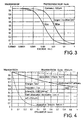
- E o is the energy contained in the laser pulse, ⁇ L , W o respectively represent the width of the pulse and the dimension of the radius of the laser beam at 1 / e (case of a Gaussian distribution).
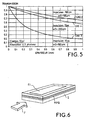
- Figures 4 and 5 show the evolution of the transmission as a function of the penetration depth of the pulse laser in the photoconductive material.
- Figure 4 corresponds to the case 1.
- Figure 5 represents cases 2, 3 and 4.
- the associated absorption described the creation of carriers and consequently the seeding in volume of carriers from a laser beam whose wavelength is located in the area of transparency of the semiconductor material.
- the transmission decreases and therefore the absorption at two photons increases when the energy of the light pulse increases (case 1).
- cases 1, 2 and 3 we notice that for an energy given light (cases 1, 2 and 3) the absorption is better with a short-lived pulse and energy density per unit area larger (case 3).
- the energy levels (and intensities) required to activate work at the photoconductive level are today accessible from miniature sources delivering laser pulses ultrashort.
- it is possible to adjust the coefficient absorption by varying the focus of the optical beam or the duration of the laser pulse.
- the duration of a pulse will be between the sub-picosecond and the sub-nanosecond. For example, it will be understood between a few fento-seconds or tens of fento-seconds and a few hundred picoseconds.
- the use of a laser operating at 1.06 ⁇ m delivering 10 ⁇ J in a pulse of 1 ps makes it possible to obtain an equivalent absorption coefficient of 10 cm -1 for an illumination spot of the order 1 mm 2 .
- the lighting can be done either directly in the inter-electrode spacing, or by the rear face.
- the limitation in this case is represented by the width of the pulse which occupies a distance of the order of 100 ⁇ m for an illumination duration of 1 ps in GaAs.
Landscapes
- Lasers (AREA)
- Optical Modulation, Optical Deflection, Nonlinear Optics, Optical Demodulation, Optical Logic Elements (AREA)
Description
- isolement galvanique de l'actuateur,
- temps de réponse intrinsèque très court, image de l'impulsion laser employée,
- absence de fluctuations dans l'instant d'établissement du courant qui est déterminé par l'apparition de la lumière.
- la figure 1, un exemple de réalisation simplifiée du dispositif de l'invention ;
- les figures 2a, 2b, des schémas d'explication du fonctionnement du dispositif de l'invention ;
- les figures 3, 4, 5, des courbes de fonctionnement du dispositif de l'invention ;
- la figure 6, un exemple de réalisation plus détaillé d'un commutateur selon l'invention.
- la section effective du faisceau laser,
- l'inverse du coefficient d'absorption (cm-1).
- Energie par impulsion couplée au matériau semiconducteur : 1mJ
- Durée impulsion : 1ns
- Dimension focalisation : 250 µm
- Energie par impulsion couplée au semiconducteur : 10 µJ
- Durée impulsion : 100 ps
- Dimension focalisation : 100 µm Intensité : 0,179 GW/cm2 (fluence = 17,95 mJ/cm2)
- Energie par impulsion couplée au semiconducteur : 10 µJ
- Durée impulsion : 10 ps
- Dimension focalisation : 100 µm Intensité : 1.796 GW/cm2 (fluence = 17,95 mJ/cm2)
- Energie par impulsion couplée au semiconducteur : 10 µJ
- Durée impulsion : 10 ps
- Dimension focalisation : 250 µm Intensité : 0.287 GW/cm2 (fluence = 2,87 mJ/cm2)
- minimisation des effets thermiques en surface et en volume = = > réduction contraintes mécaniques, ce qui influe sur la tenue mécanique et la dégradation de l'interface,
- le volume excité est plus important ce qui entraíne une réduction des effets de filamentation, de l'effet Auger, un accroissement du courant pouvant être commuté, et une diminution du poids des effets d'interface (centres de recombinaison),
- il n'est pas nécessaire d'ajuster la longueur d'onde d'excitation optique à celle associée à la fenêtre d'absorption (bordure de bande) du semiconducteur,
- il est possible d'ajuster la distribution volumique des porteurs en jouant sur la focalisation au sein du matériau semiconducteur.
- la possibilité d'emploi des techniques "Lift-off" autorisant un dépôt du matériau actif sur un substrat thermiquement adapté : silicium ou saphir (transparent à 1,06 µm),
- la commande dépend de la polarisation du faisceau excitateur (règle de sélection : couplage ondes électromagnétiques aux transitions électron-trou lourd/électron-trou léger),
- le confinement optique est propice à l'exploitation de l'absorption à deux photons,
- la longueur d'interaction peut être importante et l'emploi de structures évasées au niveau du guide permet de distribuer la densité de porteurs photoinduits,
- enfin, cette géométrie autorise l'empilement ("stacking") de multicommutateurs à commande optique unique.
Claims (11)
- Commutateur électrique à photoconducteur comprenant un élément en matériau photoconducteur (1) possédant deux électrodes (2, 2') situées de part et d'autre d'une zone active (3), au moins une source lumineuse (4) émettant au moins un faisceau lumineux (5) éclairant la zone active (3), le faisceau (5) ayant une longueur d'onde correspondant à une énergie photonique inférieure à l'énergie de bande interdite du matériau photoconducteur (1), l'intensité du faisceau lumineux étant telle qu'il y ait combinaison de l'énergie d'au moins deux photons dans le matériau photoconducteur de façon qu'un mécanisme d'absorption à 2 photons dans le matériau photoconducteur contribue à la création de porteurs permettant de rendre conducteur le matériau photoconducteur.
- Commutateur selon la revendication 1, caractérisé en ce que le faisceau a une longueur d'onde dont la valeur de l'énergie photonique est comprise entre la moitié de l'énergie de bande interdite du matériau photoconducteur et l'énergie de bande interdite du matériau.
- Commutateur selon la revendication 1, caractérisé en ce que l'intensité du faisceau lumineux (5) a une valeur permettant une absorption photonique à deux photons dans le matériau photoconducteur.
- Commutateur selon la revendication 3, caractérisé en ce que le faisceau lumineux (5) est transmis sous forme d'impulsions lumineuses dont la durée est de l'ordre de la sub-picoseconde à la sub-nanoseconde.
- Commutateur selon la revendication 1, caractérisé en ce que la focalisation du faisceau lumineux sur le matériau photoconducteur est contrôlable.
- Commutateur selon la revendication 1, caractérisé en ce que la source (4) est un laser dopé néodyme permettant une émission d'un faisceau lumineux à une longueur d'onde de 1,064 ou 1,32 µm.
- Commutateur selon la revendication 1, caractérisé en ce que le matériau photoconducteur est du GaAs.
- Commutateur selon la revendication 1, caractérisé en ce que l'élément en matériau photoconducteur (1) est de forme plane et en ce que la zone active éclairée par le faisceau lumineux est situé sur une face principale plane de l'élément.
- Commutateur selon la revendication 8, caractérisé en ce que l'élément en matériau photoconducteur (1) est de forme plane et en ce qu'il est éclairé par l'une de ses tranches par le faisceau lumineux (5).
- Commutateur selon la revendication 1, caractérisé en ce que le matériau photoconducteur est en AsGa, la source laser est un laser YAG dopé néodyme.
- Commutateur selon la revendication 1, caractérisé en ce que la durée de l'impulsion lumineuse est de l'ordre de 10 ps ou inférieure à 10 ps et que la fluence optique incidente est supérieure à 1,5 mJ/cm2.
Applications Claiming Priority (2)
| Application Number | Priority Date | Filing Date | Title |
|---|---|---|---|
| FR9607079A FR2749721B1 (fr) | 1996-06-07 | 1996-06-07 | Commutateur electrique a photoconducteur |
| FR9607079 | 1996-06-07 |
Publications (2)
| Publication Number | Publication Date |
|---|---|
| EP0812067A1 EP0812067A1 (fr) | 1997-12-10 |
| EP0812067B1 true EP0812067B1 (fr) | 2003-10-22 |
Family
ID=9492824
Family Applications (1)
| Application Number | Title | Priority Date | Filing Date |
|---|---|---|---|
| EP97401138A Expired - Lifetime EP0812067B1 (fr) | 1996-06-07 | 1997-05-23 | Commutateur électrique à photoconducteur |
Country Status (4)
| Country | Link |
|---|---|
| US (1) | US5912455A (fr) |
| EP (1) | EP0812067B1 (fr) |
| DE (1) | DE69725649T2 (fr) |
| FR (1) | FR2749721B1 (fr) |
Families Citing this family (11)
| Publication number | Priority date | Publication date | Assignee | Title |
|---|---|---|---|---|
| EP1064750A4 (fr) | 1998-02-25 | 2004-12-08 | Auckland Uniservices Ltd | Systeme et procede de demultiplexage dans des systemes de communication optique |
| FR2784185B1 (fr) | 1998-10-06 | 2001-02-02 | Thomson Csf | Dispositif pour l'harmonisation entre une voie d'emission laser et une voie passive d'observation |
| SE9900883D0 (sv) * | 1999-03-12 | 1999-03-12 | Asea Brown Boveri | A photoconductive switch |
| US6107643A (en) * | 1999-03-24 | 2000-08-22 | Abb Ab | Photoconductive switch with doping adapted to the intensity distribution of an illumination source thereof |
| FR2814281B1 (fr) * | 2000-09-19 | 2003-08-29 | Thomson Lcd | Matrice active tft pour capteur optique comportant une couche semi-conductrice photosensible, et capteur optique comportant une telle matrice |
| AT411503B8 (de) * | 2002-02-28 | 2004-05-25 | Femtolasers Produktions Gmbh | Einrichtung zur erzeugung von terahertz-strahlung sowie halbleiterbauelement |
| JP3913253B2 (ja) * | 2004-07-30 | 2007-05-09 | キヤノン株式会社 | 光半導体装置およびその製造方法 |
| DE102005021298A1 (de) * | 2005-05-09 | 2006-11-16 | Rohde & Schwarz Gmbh & Co. Kg | Optoelektronisch gesteuerter Schalter oder Modulator und Abschwächer |
| CN1877866B (zh) * | 2006-07-06 | 2010-07-28 | 胡思福 | 半导体光电导开关及其制备方法 |
| US10191353B2 (en) * | 2017-03-29 | 2019-01-29 | Lawrence Livermore National Security, Llc | Optically triggered electrical switches with fast recovery based on nonlinear optical response |
| JP7651502B2 (ja) * | 2022-03-23 | 2025-03-26 | 株式会社東芝 | 光スイッチ |
Family Cites Families (17)
| Publication number | Priority date | Publication date | Assignee | Title |
|---|---|---|---|---|
| US3801825A (en) * | 1968-07-15 | 1974-04-02 | Sanders Associates Inc | Apparatus for detecting coherent radiant energy |
| US3620597A (en) * | 1968-07-15 | 1971-11-16 | Sanders Associates Inc | Method and apparatus for nonlinear optical limiting |
| GB1466676A (en) * | 1974-02-02 | 1977-03-09 | Bleach J A | Solid state relay |
| GB2131227B (en) * | 1982-11-26 | 1987-01-07 | Walter Margulis | Apparatus for measuring light beam characteristics |
| JPS59112233A (ja) * | 1982-11-26 | 1984-06-28 | ナショナル・リサ−チ・ディベロプメント・コ−ポレ−ション | 光ビ−ム特性測定装置 |
| FR2619936B1 (fr) * | 1987-09-01 | 1989-12-01 | Thomson Csf | Modulateur pour onde electromagnetique, a puits quantiques, et utilisation de ce modulateur comme polariseur |
| FR2619938B1 (fr) * | 1987-09-01 | 1989-12-01 | Thomson Csf | Translateur de frequence pour onde du domaine infrarouge moyen |
| FR2622706B1 (fr) * | 1987-11-03 | 1992-01-17 | Thomson Csf | Dispositif d'interconnexion optique dynamique pour circuits integres |
| US5332918A (en) * | 1988-02-19 | 1994-07-26 | Massachusetts Institute Of Technology | Ultra-high-speed photoconductive devices using semi-insulating layers |
| US5325324A (en) * | 1989-04-25 | 1994-06-28 | Regents Of The University Of California | Three-dimensional optical memory |
| FR2649536B1 (fr) * | 1989-07-04 | 1994-07-22 | Thomson Csf | Detecteur d'ondes electromagnetiques |
| FR2667207B1 (fr) * | 1990-09-21 | 1993-06-25 | Thomson Csf | Convertisseur de frequences lumineuses. |
| JP3176644B2 (ja) * | 1991-03-27 | 2001-06-18 | 浜松ホトニクス株式会社 | 光波形の測定装置 |
| FR2686431A1 (fr) * | 1992-01-21 | 1993-07-23 | Thomson Csf | Doubleur de frequence optique utilisant des structures quantiques semiconductrices. |
| US5258612A (en) * | 1992-04-01 | 1993-11-02 | Clark William G | Timed-resolved spectroscopy with split pump and probe pulses |
| FR2715776B1 (fr) * | 1994-01-28 | 1996-03-01 | Thomson Csf Semiconducteurs | Laser de grande puissance à deux étages. |
| US5757992A (en) * | 1996-09-09 | 1998-05-26 | Lucent Technologies Inc. | Fiber optic communication system and method |
-
1996
- 1996-06-07 FR FR9607079A patent/FR2749721B1/fr not_active Expired - Lifetime
-
1997
- 1997-05-07 US US08/852,686 patent/US5912455A/en not_active Expired - Lifetime
- 1997-05-23 EP EP97401138A patent/EP0812067B1/fr not_active Expired - Lifetime
- 1997-05-23 DE DE69725649T patent/DE69725649T2/de not_active Expired - Lifetime
Also Published As
| Publication number | Publication date |
|---|---|
| US5912455A (en) | 1999-06-15 |
| EP0812067A1 (fr) | 1997-12-10 |
| FR2749721A1 (fr) | 1997-12-12 |
| DE69725649D1 (de) | 2003-11-27 |
| DE69725649T2 (de) | 2004-09-30 |
| FR2749721B1 (fr) | 1998-11-27 |
Similar Documents
| Publication | Publication Date | Title |
|---|---|---|
| EP0812067B1 (fr) | Commutateur électrique à photoconducteur | |
| Zhao et al. | Ultrafast control of slow light in THz electromagnetically induced transparency metasurfaces | |
| EP0369856B1 (fr) | Dispositif optoélectronique de puissance, et son procédé de réalisation | |
| FR3041816A1 (fr) | Generateur solaire flexible muni d'une protection electrique contre des impacts d'objets celestes, engin spatial et satellite comportant au moins un tel generateur solaire | |
| EP1151507A1 (fr) | Dispositif emetteur de lumiere, en silicium et procede de fabrication | |
| EP0007878A1 (fr) | Générateur photovoltaique | |
| CA1272790A (fr) | Generateur laser a gaz | |
| EP2700133A1 (fr) | Dispostif laser d'emission d'ondes dans le domaine des terahertz | |
| FR2787246A1 (fr) | Laser de type semi-conducteur | |
| FR2697679A1 (fr) | Déphaseur d'ondes électromagnétiques et application à une antenne à balayage électronique. | |
| FR2690005A1 (fr) | Canon à électrons compact comportant une source d'électrons à micropointes et laser à semi-conducteur utilisant ce canon pour le pompage électronique. | |
| EP0298817B1 (fr) | Procédé et dispositif de production d'électrons utilisant un couplage de champ et l'effet photoélectrique | |
| FR2716040A1 (fr) | Commande de diode laser pulsée, compacte, à fréquence de répétition d'impulsion élévée et de grande puissance. | |
| TWI283931B (en) | Optical transistor | |
| JP4786010B2 (ja) | 集積型ハイブリッド薄膜太陽電池の製造方法 | |
| EP0534821B1 (fr) | Lasers de puissance à filtre semiconducteur | |
| US6628680B2 (en) | Photoconductive switch with integral wavelength converter | |
| FR2761537A1 (fr) | Laser comprenant un empilement de diodes laser epitaxiees compris entre deux miroirs de bragg | |
| JP2008140990A (ja) | 光電変換装置 | |
| EP0524878A1 (fr) | Absorbeur hyperfréquence à semiconducteur et à commande optique | |
| JPWO2005047964A1 (ja) | 光制御装置 | |
| EP1966888B1 (fr) | Generateur d'impulsions electriques de forte puissance | |
| EP0203848B1 (fr) | Procédé de fabrication d'un laser à semiconducteur à géométrie à ruban et laser obtenu par ce procédé | |
| JP2008141075A (ja) | テラヘルツ電磁波発生装置 | |
| FR2987179A1 (fr) | Source laser a declenchement actif |
Legal Events
| Date | Code | Title | Description |
|---|---|---|---|
| PUAI | Public reference made under article 153(3) epc to a published international application that has entered the european phase |
Free format text: ORIGINAL CODE: 0009012 |
|
| AK | Designated contracting states |
Kind code of ref document: A1 Designated state(s): CH DE GB LI |
|
| 17P | Request for examination filed |
Effective date: 19980312 |
|
| RAP1 | Party data changed (applicant data changed or rights of an application transferred) |
Owner name: THALES |
|
| GRAH | Despatch of communication of intention to grant a patent |
Free format text: ORIGINAL CODE: EPIDOS IGRA |
|
| GRAS | Grant fee paid |
Free format text: ORIGINAL CODE: EPIDOSNIGR3 |
|
| GRAA | (expected) grant |
Free format text: ORIGINAL CODE: 0009210 |
|
| AK | Designated contracting states |
Kind code of ref document: B1 Designated state(s): CH DE GB LI |
|
| REG | Reference to a national code |
Ref country code: GB Ref legal event code: FG4D Free format text: NOT ENGLISH |
|
| REG | Reference to a national code |
Ref country code: CH Ref legal event code: EP |
|
| REF | Corresponds to: |
Ref document number: 69725649 Country of ref document: DE Date of ref document: 20031127 Kind code of ref document: P |
|
| GBT | Gb: translation of ep patent filed (gb section 77(6)(a)/1977) |
Effective date: 20040211 |
|
| PLBE | No opposition filed within time limit |
Free format text: ORIGINAL CODE: 0009261 |
|
| STAA | Information on the status of an ep patent application or granted ep patent |
Free format text: STATUS: NO OPPOSITION FILED WITHIN TIME LIMIT |
|
| 26N | No opposition filed |
Effective date: 20040723 |
|
| PGFP | Annual fee paid to national office [announced via postgrant information from national office to epo] |
Ref country code: CH Payment date: 20130514 Year of fee payment: 17 Ref country code: DE Payment date: 20130515 Year of fee payment: 17 Ref country code: GB Payment date: 20130522 Year of fee payment: 17 |
|
| REG | Reference to a national code |
Ref country code: DE Ref legal event code: R119 Ref document number: 69725649 Country of ref document: DE |
|
| REG | Reference to a national code |
Ref country code: CH Ref legal event code: PL |
|
| GBPC | Gb: european patent ceased through non-payment of renewal fee |
Effective date: 20140523 |
|
| PG25 | Lapsed in a contracting state [announced via postgrant information from national office to epo] |
Ref country code: CH Free format text: LAPSE BECAUSE OF NON-PAYMENT OF DUE FEES Effective date: 20140531 Ref country code: LI Free format text: LAPSE BECAUSE OF NON-PAYMENT OF DUE FEES Effective date: 20140531 |
|
| REG | Reference to a national code |
Ref country code: DE Ref legal event code: R119 Ref document number: 69725649 Country of ref document: DE Effective date: 20141202 |
|
| PG25 | Lapsed in a contracting state [announced via postgrant information from national office to epo] |
Ref country code: DE Free format text: LAPSE BECAUSE OF NON-PAYMENT OF DUE FEES Effective date: 20141202 |
|
| PG25 | Lapsed in a contracting state [announced via postgrant information from national office to epo] |
Ref country code: GB Free format text: LAPSE BECAUSE OF NON-PAYMENT OF DUE FEES Effective date: 20140523 |