EP0812067B1 - Photoconductive electric switch - Google Patents
Photoconductive electric switch Download PDFInfo
- Publication number
- EP0812067B1 EP0812067B1 EP97401138A EP97401138A EP0812067B1 EP 0812067 B1 EP0812067 B1 EP 0812067B1 EP 97401138 A EP97401138 A EP 97401138A EP 97401138 A EP97401138 A EP 97401138A EP 0812067 B1 EP0812067 B1 EP 0812067B1
- Authority
- EP
- European Patent Office
- Prior art keywords
- photoconductive material
- switch according
- light beam
- energy
- photoconductive
- Prior art date
- Legal status (The legal status is an assumption and is not a legal conclusion. Google has not performed a legal analysis and makes no representation as to the accuracy of the status listed.)
- Expired - Lifetime
Links
- 239000000463 material Substances 0.000 claims description 40
- 238000010521 absorption reaction Methods 0.000 claims description 35
- 230000003287 optical effect Effects 0.000 claims description 14
- 239000000969 carrier Substances 0.000 claims description 11
- JBRZTFJDHDCESZ-UHFFFAOYSA-N AsGa Chemical compound [As]#[Ga] JBRZTFJDHDCESZ-UHFFFAOYSA-N 0.000 claims description 8
- 229910001218 Gallium arsenide Inorganic materials 0.000 claims description 6
- 230000007246 mechanism Effects 0.000 claims description 6
- 229910017214 AsGa Inorganic materials 0.000 claims description 2
- 239000004065 semiconductor Substances 0.000 description 18
- 230000000694 effects Effects 0.000 description 7
- 230000005540 biological transmission Effects 0.000 description 6
- 230000005284 excitation Effects 0.000 description 6
- 238000000034 method Methods 0.000 description 4
- XUIMIQQOPSSXEZ-UHFFFAOYSA-N Silicon Chemical compound [Si] XUIMIQQOPSSXEZ-UHFFFAOYSA-N 0.000 description 3
- 230000008901 benefit Effects 0.000 description 3
- 230000003993 interaction Effects 0.000 description 3
- 230000009467 reduction Effects 0.000 description 3
- 239000007787 solid Substances 0.000 description 3
- 230000007704 transition Effects 0.000 description 3
- 239000000835 fiber Substances 0.000 description 2
- 238000005286 illumination Methods 0.000 description 2
- 230000035515 penetration Effects 0.000 description 2
- 230000008569 process Effects 0.000 description 2
- 229910052710 silicon Inorganic materials 0.000 description 2
- 239000010703 silicon Substances 0.000 description 2
- 239000000758 substrate Substances 0.000 description 2
- 239000011149 active material Substances 0.000 description 1
- 229910045601 alloy Inorganic materials 0.000 description 1
- 239000000956 alloy Substances 0.000 description 1
- 230000015556 catabolic process Effects 0.000 description 1
- 150000001875 compounds Chemical class 0.000 description 1
- 230000008878 coupling Effects 0.000 description 1
- 238000010168 coupling process Methods 0.000 description 1
- 238000005859 coupling reaction Methods 0.000 description 1
- 230000007423 decrease Effects 0.000 description 1
- 238000006731 degradation reaction Methods 0.000 description 1
- 230000008021 deposition Effects 0.000 description 1
- 238000010586 diagram Methods 0.000 description 1
- 230000002349 favourable effect Effects 0.000 description 1
- 230000004907 flux Effects 0.000 description 1
- 239000011521 glass Substances 0.000 description 1
- 238000002955 isolation Methods 0.000 description 1
- 239000011159 matrix material Substances 0.000 description 1
- 238000010899 nucleation Methods 0.000 description 1
- 238000013021 overheating Methods 0.000 description 1
- 230000010287 polarization Effects 0.000 description 1
- 230000006798 recombination Effects 0.000 description 1
- 238000005215 recombination Methods 0.000 description 1
- 230000004044 response Effects 0.000 description 1
- 229910052594 sapphire Inorganic materials 0.000 description 1
- 239000010980 sapphire Substances 0.000 description 1
- 230000003595 spectral effect Effects 0.000 description 1
Images


Classifications
-
- H—ELECTRICITY
- H03—ELECTRONIC CIRCUITRY
- H03K—PULSE TECHNIQUE
- H03K17/00—Electronic switching or gating, i.e. not by contact-making and –breaking
- H03K17/51—Electronic switching or gating, i.e. not by contact-making and –breaking characterised by the components used
- H03K17/78—Electronic switching or gating, i.e. not by contact-making and –breaking characterised by the components used using opto-electronic devices, i.e. light-emitting and photoelectric devices electrically- or optically-coupled
-
- H—ELECTRICITY
- H01—ELECTRIC ELEMENTS
- H01L—SEMICONDUCTOR DEVICES NOT COVERED BY CLASS H10
- H01L31/00—Semiconductor devices sensitive to infrared radiation, light, electromagnetic radiation of shorter wavelength or corpuscular radiation and specially adapted either for the conversion of the energy of such radiation into electrical energy or for the control of electrical energy by such radiation; Processes or apparatus specially adapted for the manufacture or treatment thereof or of parts thereof; Details thereof
- H01L31/08—Semiconductor devices sensitive to infrared radiation, light, electromagnetic radiation of shorter wavelength or corpuscular radiation and specially adapted either for the conversion of the energy of such radiation into electrical energy or for the control of electrical energy by such radiation; Processes or apparatus specially adapted for the manufacture or treatment thereof or of parts thereof; Details thereof in which radiation controls flow of current through the device, e.g. photoresistors
Definitions
- the invention relates to an electrical switch with photoconductor.
- Photoconductive electrical switching consists in connecting two circuit elements by a semiconductor material, strongly insulating in the dark, and making the connection by submitting this solid to a luminous flux which makes it conductive. Conduction thus results from photo-creation of electrically charged carriers (electrons and holes).
- the optical control source is represented by a laser.
- the photoconductor In the case of high power electrical pulses (for example at the MW scale), the photoconductor is subjected to high currents (kA). It is therefore desirable to have a photoconductor with a large section (for example a few mm 2 ). Furthermore, the switching of high voltages (kV) implies the use of switching structures of sufficient length (a few mm) in order to avoid reaching the breaking field of the material. All the dimensions are then of the order (or greater) per mm and it is desired to create load carriers throughout the volume.
- the optical absorption of semiconductor materials at a given wavelength is generally either very low (photon energy lower than that of the bandgap energy of the material), or very high (absorption coefficient) of several hundred cm -1 as soon as the photon energy is greater than that associated with the band gap).
- the search for intermediate values of the absorption coefficient requires a relatively precise agreement between the excitation wavelength (laser) and the threshold wavelength of the semiconductor (associated with the band gap energy); agreement which is generally not achieved.
- the absorption being very high, it is made of generally on the surface of the material.
- the thickness of ionized material is then very weak.
- the section of the material perpendicular to the direction switching and therefore to the flow of a current to be switched is very weak. If you want to switch a very high current, the material may deteriorate in the absorption area due to overheating due to current flow.
- Some semiconductors such as silicon have lower absorption coefficients at shorter wavelengths at the absorption threshold (compared to GaAs). They present a limitation to high power switching. In addition, characteristics of the carriers in these semiconductors are few favorable for efficient switching (low mobility of carriers).
- the subject of the invention is therefore an electric switch with photoconductor allowing switching of high currents.
- an electric photoconductive switch comprising an element of photoconductive material having two electrodes located on either side of an active area, at least one light source emitting at least one light beam illuminating the active area, the beam having a wavelength corresponding to a photon energy lower than the bandgap energy of the material photoconductor, the intensity of the light beam being such that there is combination of the energy of at least two photons in the material photoconductor.
- An element made of photoconductive material 1 has two opposite ends, two electrodes 2, 2 '. Between these two electrodes, an area 3 is illuminated by a beam 5 emitted by a source 4.
- the wavelength of beam 5 is such that its energy photonics is less than or equal to the bandwidth energy prohibited photoconductive material 1.
- the optical intensity of the beam is such that it gives rise to an absorption phenomenon at two photons or else, expressed differently, so that the sum of energies of two photons correspond to the band gap energy of the photoconductive material.
- the effective distance over which the carriers are generated is of the millimeter type, which makes it possible to produce a volume plasma rather than surface.
- the absorption phenomenon at two photons (A2P) is used in this perspective.
- the two-photon absorption mechanism translates the excitation of a semiconductor material in the transparency range thereof.
- the effect of the wavelength is shown diagrammatically in FIGS. 2a and 2b.
- This non-linear phenomenon appears for a high density of light excitement. Its operation is based on the existence of a virtual level of short life. This mechanism is all the more effective that the optical control intensity is applied to the material semiconductor in short pulse regime.
- This source can be represented by an Er 3+ doped glass laser or by a laser fiber (with fiber amplifier).
- E o is the energy contained in the laser pulse, ⁇ L , W o respectively represent the width of the pulse and the dimension of the radius of the laser beam at 1 / e (case of a Gaussian distribution).
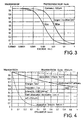
- Figures 4 and 5 show the evolution of the transmission as a function of the penetration depth of the pulse laser in the photoconductive material.
- Figure 4 corresponds to the case 1.
- Figure 5 represents cases 2, 3 and 4.
- the associated absorption described the creation of carriers and consequently the seeding in volume of carriers from a laser beam whose wavelength is located in the area of transparency of the semiconductor material.
- the transmission decreases and therefore the absorption at two photons increases when the energy of the light pulse increases (case 1).
- cases 1, 2 and 3 we notice that for an energy given light (cases 1, 2 and 3) the absorption is better with a short-lived pulse and energy density per unit area larger (case 3).
- the energy levels (and intensities) required to activate work at the photoconductive level are today accessible from miniature sources delivering laser pulses ultrashort.
- it is possible to adjust the coefficient absorption by varying the focus of the optical beam or the duration of the laser pulse.
- the duration of a pulse will be between the sub-picosecond and the sub-nanosecond. For example, it will be understood between a few fento-seconds or tens of fento-seconds and a few hundred picoseconds.
- the use of a laser operating at 1.06 ⁇ m delivering 10 ⁇ J in a pulse of 1 ps makes it possible to obtain an equivalent absorption coefficient of 10 cm -1 for an illumination spot of the order 1 mm 2 .
- the lighting can be done either directly in the inter-electrode spacing, or by the rear face.
- the limitation in this case is represented by the width of the pulse which occupies a distance of the order of 100 ⁇ m for an illumination duration of 1 ps in GaAs.
Description
L'invention concerne un commutateur électrique à photoconducteur.The invention relates to an electrical switch with photoconductor.
La commutation électrique à photoconducteur consiste à relier deux éléments de circuit par un matériau semiconducteur, fortement isolant dans l'obscurité, et à établir la connexion en soumettant ce solide à un flux lumineux qui le rend conducteur. La conduction résulte ainsi de la photo-création de porteurs chargés électriquement (électrons et trous).Photoconductive electrical switching consists in connecting two circuit elements by a semiconductor material, strongly insulating in the dark, and making the connection by submitting this solid to a luminous flux which makes it conductive. Conduction thus results from photo-creation of electrically charged carriers (electrons and holes).
La commutation électrique à photoconducteur présente un certain nombre d'avantages comparativement aux autres modes de commande (mécanique, arcs électriques et décharge dans les gaz, ...).
- isolement galvanique de l'actuateur,
- temps de réponse intrinsèque très court, image de l'impulsion laser employée,
- absence de fluctuations dans l'instant d'établissement du courant qui est déterminé par l'apparition de la lumière.
- galvanic isolation of the actuator,
- very short intrinsic response time, image of the laser pulse used,
- absence of fluctuations in the instant of establishment of the current which is determined by the appearance of light.
La source optique de commande est représentée par un laser. Aujourd'hui, on réalise des impulsions ultracourtes optiques (quelques 10-15s) à partir de telles sources, ce qui permet d'obtenir des impulsions électriques à transitions très abruptes.The optical control source is represented by a laser. Today, ultrashort optical pulses (some 10 -15 s) are produced from such sources, which makes it possible to obtain electrical pulses with very steep transitions.
Dans le cas d'impulsions électriques de grande puissance (par exemple à l'échelle du MW), le photoconducteur est soumis à des courants élevés (kA). Il est alors souhaitable de disposer d'un photoconducteur de grande section (par exemple quelques mm2). Par ailleurs, la commutation de fortes tensions (kV) implique l'emploi de structures de commutation de longueur suffisante (quelques mm) afin d'éviter d'atteindre le champ de rupture du matériau. Toutes les dimensions sont alors de l'ordre (ou supérieures) au mm et l'on souhaite créer des porteurs de charge dans l'ensemble du volume.In the case of high power electrical pulses (for example at the MW scale), the photoconductor is subjected to high currents (kA). It is therefore desirable to have a photoconductor with a large section (for example a few mm 2 ). Furthermore, the switching of high voltages (kV) implies the use of switching structures of sufficient length (a few mm) in order to avoid reaching the breaking field of the material. All the dimensions are then of the order (or greater) per mm and it is desired to create load carriers throughout the volume.
L'absorption optique des matériaux semiconducteurs à une longueur d'onde donnée est en général soit très faible (énergie du photon inférieure à celle de l'énergie de bande interdite du matériau), soit très élevée (coefficient d'absorption) de plusieurs centaines de cm-1 dès que l'énergie du photon est plus grande que celle associée à la bande interdite). La recherche de valeurs intermédiaires du coefficient d'absorption exige un accord relativement précis entre la longueur d'onde d'excitation (laser) et la longueur d'onde seuil du semiconducteur (associée à l'énergie de bande interdite) ; accord qui n'est en général pas réalisé.The optical absorption of semiconductor materials at a given wavelength is generally either very low (photon energy lower than that of the bandgap energy of the material), or very high (absorption coefficient) of several hundred cm -1 as soon as the photon energy is greater than that associated with the band gap). The search for intermediate values of the absorption coefficient requires a relatively precise agreement between the excitation wavelength (laser) and the threshold wavelength of the semiconductor (associated with the band gap energy); agreement which is generally not achieved.
Par ailleurs, l'absorption étant très élevée, elle se fait de manière générale en surface du matériau. L'épaisseur de matériau ionisé est alors très faible. La section du matériau perpendiculaire à la direction de commutation et donc à la circulation d'un courant à commuter est très faible. S'il s'agit de commuter un courant à très forte intensité, le matériau risque d'être détérioré dans la zone d'absorption en raison de l'échauffement dû au passage du courant.Furthermore, the absorption being very high, it is made of generally on the surface of the material. The thickness of ionized material is then very weak. The section of the material perpendicular to the direction switching and therefore to the flow of a current to be switched is very weak. If you want to switch a very high current, the material may deteriorate in the absorption area due to overheating due to current flow.
Certains semiconducteurs tel que le silicium présentent des coefficients d'absorption plus faibles aux longueurs d'ondes inférieures au seuil d'absorption (comparativement à GaAs). Ils présentent une limitation à la commutation de forte puissance. Par ailleurs, les caractéristiques des porteurs dans ces semiconducteurs sont peu favorables à l'obtention d'une commutation efficace (faible mobilité des porteurs).Some semiconductors such as silicon have lower absorption coefficients at shorter wavelengths at the absorption threshold (compared to GaAs). They present a limitation to high power switching. In addition, characteristics of the carriers in these semiconductors are few favorable for efficient switching (low mobility of carriers).
L'invention a donc pour objet un commutateur électrique à photoconducteur permettant une commutation de courants élevés.The subject of the invention is therefore an electric switch with photoconductor allowing switching of high currents.
Elle concerne un commutateur électrique à photoconducteur comprenant un élément en matériau photoconducteur possédant deux électrodes situées de part et d'autre d'une zone active, au moins une source lumineuse émettant au moins un faisceau lumineux éclairant la zone active, le faisceau ayant une longueur d'onde correspondant à une énergie photonique inférieure à l'énergie de bande interdite du matériau photoconducteur, l'intensité du faisceau lumineux étant telle qu'il y ait combinaison de l'énergie d'au moins deux photons dans le matériau photoconducteur.It relates to an electric photoconductive switch comprising an element of photoconductive material having two electrodes located on either side of an active area, at least one light source emitting at least one light beam illuminating the active area, the beam having a wavelength corresponding to a photon energy lower than the bandgap energy of the material photoconductor, the intensity of the light beam being such that there is combination of the energy of at least two photons in the material photoconductor.
Les différents objets et caractéristiques de l'invention apparaítront plus clairement dans la description qui va suivre et dans les figures annexées qui représentent :
- la figure 1, un exemple de réalisation simplifiée du dispositif de l'invention ;
- les figures 2a, 2b, des schémas d'explication du fonctionnement du dispositif de l'invention ;
- les figures 3, 4, 5, des courbes de fonctionnement du dispositif de l'invention ;
- la figure 6, un exemple de réalisation plus détaillé d'un commutateur selon l'invention.
- Figure 1, a simplified embodiment of the device of the invention;
- Figures 2a, 2b, diagrams of explanation of the operation of the device of the invention;
- Figures 3, 4, 5, operating curves of the device of the invention;
- Figure 6, a more detailed embodiment of a switch according to the invention.
En se reportant à la figure 1, on va tout d'abord décrire un exemple de réalisation simplifiée du commutateur selon l'invention.Referring to Figure 1, we will first describe a simplified embodiment of the switch according to the invention.
Un élément en matériau photoconducteur 1 possède, à deux
extrémités opposées, deux électrodes 2, 2'. Entre ces deux électrodes,
une zone 3 est éclairée par un faisceau 5 émis par une source 4. A titre
d'exemple, la longueur d'onde du faisceau 5 est telle que son énergie
photonique est inférieure ou égale à l'énergie de largeur de bande
interdite du matériau photoconducteur 1. De plus, l'intensité optique du
faisceau est telle qu'elle donne lieu à un phénomène d'absorption à deux
photons ou bien, exprimé autrement, de telle façon que la somme des
énergies de deux photons corresponde à l'énergie de bande interdite du
matériau photoconducteur.An element made of
La distance effective sur laquelle sont générés les porteurs est de type millimétrique, ce qui permet de réaliser un plasma volumique plutôt que surfacique. Selon l'invention, le phénomène d'absorption à deux photons (A2P) est employé dans cette perspective.The effective distance over which the carriers are generated is of the millimeter type, which makes it possible to produce a volume plasma rather than surface. According to the invention, the absorption phenomenon at two photons (A2P) is used in this perspective.
Le mécanisme d'absorption à deux photons traduit l'excitation d'un matériau semiconducteur dans le domaine de transparence de celui-ci. L'effet de la longueur d'onde est schématisé sur les figures 2a et 2b.The two-photon absorption mechanism translates the excitation of a semiconductor material in the transparency range thereof. The effect of the wavelength is shown diagrammatically in FIGS. 2a and 2b.
Ce phénomène non-linéaire apparaít pour une forte densité d'excitation lumineuse. Son fonctionnement repose sur l'existence d'un niveau virtuel de durée de vie courte. Ce mécanisme est d'autant plus efficace que l'intensité optique de commande est appliquée au matériau semiconducteur en régime impulsionnel court.This non-linear phenomenon appears for a high density of light excitement. Its operation is based on the existence of a virtual level of short life. This mechanism is all the more effective that the optical control intensity is applied to the material semiconductor in short pulse regime.
On considère le matériau GaAs qui présente une énergie de bande interdite située au voisinage de 1,424 eV. Un photon issu d'un laser Nd:YAG (ou autre matrice) présente une énergie de 1,165 eV et l'absorption à deux photons correspond à 2,33 eV (figure 2a). We consider the GaAs material which has an energy of prohibited band located near 1,424 eV. A photon from a Nd: YAG laser (or other matrix) has an energy of 1.165 eV and the two-photon absorption corresponds to 2.33 eV (Figure 2a).
L'emploi d'une source opérant vers 1,55 µm (énergie du photon = 0,8 eV) permet d'atteindre 1,6 eV selon le processus non-linéaire d'absorption (figure 2b). Cette source peut être représentée par un laser verre dopé Er3+ ou par une fibre laser (avec amplificateur fibré).The use of a source operating at around 1.55 µm (photon energy = 0.8 eV) makes it possible to reach 1.6 eV according to the non-linear absorption process (Figure 2b). This source can be represented by an Er 3+ doped glass laser or by a laser fiber (with fiber amplifier).
En négligeant l'absorption par les porteurs, l'évolution de
l'intensité optique dans le milieu suit la loi :
Eo : est l'énergie contenue dans l'impulsion laser, τL, Wo représentent respectivement la largeur de l'impulsion et la dimension du rayon du faisceau laser à 1/e (cas d'une distribution gaussienne).E o : is the energy contained in the laser pulse, τ L , W o respectively represent the width of the pulse and the dimension of the radius of the laser beam at 1 / e (case of a Gaussian distribution).
A titre d'exemple, on considère le matériau semiconducteur GaAs massif non dopé à haute pureté. Le coefficient d'absorption à la longueur d'onde λ = 1,06 µm est typiquement compris entre α = 0,6 cm-1 et 1,2 cm-1. Le coefficient d'absorption à deux photons obtenu expérimentalement βexp est de l'ordre de 20 cm/GW.By way of example, we consider the solid semiconductor material GaAs undoped with high purity. The absorption coefficient at the wavelength λ = 1.06 µm is typically between α = 0.6 cm -1 and 1.2 cm -1 . The two-photon absorption coefficient obtained experimentally β exp is around 20 cm / GW.
Ce mode de fonctionnement ainsi décrit peut être réalisé à partir de matériaux et alliages semiconducteurs variés permettant de mettre en oeuvre cette architecture sur un large domaine spectral. Le volume excité est défini par :
- la section effective du faisceau laser,
- l'inverse du coefficient d'absorption (cm-1).
- the effective cross section of the laser beam,
- the inverse of the absorption coefficient (cm -1 ).
On considère la transmission lumineuse d'une plaquette
d'arséniure de gallium d'épaisseur 500 µm. En tenant compte de
l'absorption à deux photons, on calcule l'évolution de la transmission en
fonction de l'énergie contenue dans l'impulsion lumineuse de
commande. A la longueur d'onde 1,064 µm, en fonction de la largeur de
l'impulsion on obtient les courbes de transmission présentées sur la
figure 3. Le rayon de focalisation est de 50 µm et le coefficient de perte
linéaire résiduel est de 1cm-1. On observe que 90 % de l'énergie est
absorbée selon le processus d'absorption à deux photons pour une
énergie laser de 10 µJ contenue dans une impulsion de durée 10 ps
interagissant avec le composé semiconducteur. Cette efficacité montre
que le mécanisme d'absorption à deux photons peut être exploité pour
engendrer au sein du photoconducteur des paires électrons-trous qui
contribuent à réaliser un plasma de conduction en volume. Par contre,
pour atteindre le taux d'absorption de 90 % avec une impulsion de
durée de 100 ps, il faut une énergie de 100 µJ.We consider the light transmission of a 500 µm thick gallium arsenide wafer. Taking into account the two-photon absorption, the evolution of the transmission is calculated as a function of the energy contained in the control light pulse. At the wavelength 1.064 µm, depending on the width of the pulse, the transmission curves shown in Figure 3 are obtained. The focusing radius is 50 µm and the residual linear loss coefficient is 1cm -1 . It is observed that 90% of the energy is absorbed according to the two-photon absorption process for a laser energy of 10 μJ contained in a pulse of
Une autre représentation de l'effet consiste à évaluer la
transmission en fonction de la profondeur de pénétration de l'onde
optique dans le matériau photoconducteur (AsGa par exemple). Pour
cela, on a considéré différents cas d'excitation.
- Energie par impulsion couplée au matériau semiconducteur : 1mJ
- Durée impulsion : 1ns
- Dimension focalisation : 250 µm
- Energie par impulsion couplée au semiconducteur : 10 µJ
- Durée impulsion : 100 ps
- Dimension focalisation : 100 µm Intensité : 0,179 GW/cm2 (fluence = 17,95 mJ/cm2)
- Energie par impulsion couplée au semiconducteur : 10 µJ
- Durée impulsion : 10 ps
- Dimension focalisation : 100 µm Intensité : 1.796 GW/cm2 (fluence = 17,95 mJ/cm2)
- Energie par impulsion couplée au semiconducteur : 10 µJ
- Durée impulsion : 10 ps
- Dimension focalisation : 250 µm Intensité : 0.287 GW/cm2 (fluence = 2,87 mJ/cm2)
- Energy per pulse coupled to the semiconductor material: 1mJ
- Pulse duration: 1ns
- Focusing dimension: 250 µm
- Energy per pulse coupled to the semiconductor: 10 µJ
- Pulse duration: 100 ps
- Focusing dimension: 100 µm Intensity: 0.179 GW / cm 2 (fluence = 17.95 mJ / cm 2 )
- Energy per pulse coupled to the semiconductor: 10 µJ
- Pulse duration: 10 ps
- Focusing dimension: 100 µm Intensity: 1.796 GW / cm 2 (fluence = 17.95 mJ / cm 2 )
- Energy per pulse coupled to the semiconductor: 10 µJ
- Pulse duration: 10 ps
- Focusing dimension: 250 µm Intensity: 0.287 GW / cm 2 (fluence = 2.87 mJ / cm 2 )
Les figures 4 et 5 permettent d'observer l'évolution de la
transmission en fonction de la profondeur de pénétration de l'impulsion
laser dans le matériau photoconducteur. La figure 4 correspond au cas
1. La figure 5 représente les cas 2, 3 et 4. L'absorption associée décrit
la création de porteurs et par voie de conséquence l'ensemencement en
volume de porteurs à partir d'un faisceau laser dont la longueur d'onde
est située dans le domaine de transparence du matériau semiconducteur.
Comme on peut le voir la transmission diminue et donc l'absorption à
deux photons augmente lorsque l'énergie de l'impulsion lumineuse
augmente (cas 1). Mais surtout, on remarque que pour une énergie
lumineuse donnée (cas 1, 2 et 3) l'absorption est meilleure avec une
impulsion de courte durée et une densité d'énergie par unité de surface
plus grande (cas 3).Figures 4 and 5 show the evolution of the
transmission as a function of the penetration depth of the pulse
laser in the photoconductive material. Figure 4 corresponds to the
Les avantages du dispositif de l'invention sont :
- minimisation des effets thermiques en surface et en volume = = > réduction contraintes mécaniques, ce qui influe sur la tenue mécanique et la dégradation de l'interface,
- le volume excité est plus important ce qui entraíne une réduction des effets de filamentation, de l'effet Auger, un accroissement du courant pouvant être commuté, et une diminution du poids des effets d'interface (centres de recombinaison),
- il n'est pas nécessaire d'ajuster la longueur d'onde d'excitation optique à celle associée à la fenêtre d'absorption (bordure de bande) du semiconducteur,
- il est possible d'ajuster la distribution volumique des porteurs en jouant sur la focalisation au sein du matériau semiconducteur.
- minimization of thermal effects on the surface and in volume = => reduction of mechanical stresses, which influences the mechanical strength and degradation of the interface,
- the excited volume is greater which leads to a reduction in the filamentation effects, the Auger effect, an increase in the current which can be switched, and a reduction in the weight of the interface effects (recombination centers),
- it is not necessary to adjust the optical excitation wavelength to that associated with the absorption window (band edge) of the semiconductor,
- it is possible to adjust the volume distribution of the carriers by playing on the focusing within the semiconductor material.
Les niveaux d'énergie (et les intensités) requis pour mettre en oeuvre au niveau des photoconducteurs ce mécanisme sont aujourd'hui accessibles à partir de sources miniatures délivrant des impulsions laser ultracourtes. Par ailleurs, il est possible d'ajuster le coefficient d'absorption en jouant sur la focalisation du faisceau optique ou la durée de l'impulsion laser.The energy levels (and intensities) required to activate work at the photoconductive level this mechanism are today accessible from miniature sources delivering laser pulses ultrashort. In addition, it is possible to adjust the coefficient absorption by varying the focus of the optical beam or the duration of the laser pulse.
La durée d'une impulsion sera comprise entre la sub-picoseconde et la sub-nanoseconde. Par exemple, elle sera comprise entre quelques fento-secondes ou dizaines de fento-secondes et quelques centaines de picosecondes.The duration of a pulse will be between the sub-picosecond and the sub-nanosecond. For example, it will be understood between a few fento-seconds or tens of fento-seconds and a few hundred picoseconds.
A titre indicatif, l'emploi d'un laser opérant à 1,06 µm
délivrant 10µJ dans une impulsion de 1 ps permet d'obtenir un
coefficient d'absorption équivalent de 10 cm-1 pour une tache
d'éclairement de l'ordre de 1 mm2. L'éclairement peut se faire soit
directement dans l'espacement inter-électrodes, soit par la face arrière.
La limitation dans ce cas est représentée par la largeur de l'impulsion qui
occupe une distance de l'ordre de 100 µm pour une durée d'éclairement
de 1 ps dans GaAs.As an indication, the use of a laser operating at 1.06 µm delivering 10 µJ in a pulse of 1 ps makes it possible to obtain an equivalent absorption coefficient of 10 cm -1 for an illumination spot of the
En revanche, au niveau du seuil de dommage optique, il
s'avère que la fluence critique (J/cm2) varie selon une loi en Δτ1/2 pour
des durées d'impulsion comprises entre la centaine de ps et au-delà,
mais varie en Δτ-1 pour des impulsions ps ou subpicosecondes. La
comparaison des cas 2 et 4 montre l'intérêt que l'on a de travailler avec
des impulsions courtes en terme de fluence, pour un effet d'absorption à
2 photons.On the other hand, at the level of the optical damage threshold, it turns out that the critical fluence (J / cm 2 ) varies according to a law in Δτ 1/2 for pulse durations of between a hundred ps and beyond , but varies in Δτ -1 for ps or subpicosecond pulses. The comparison of
Nous avons décrit ce mécanisme en considérant des structures conventionnelles d'éclateurs solides. Il est également permis d'envisager l'exploitation de cette interaction en considérant une configuration s'identifiant à un guide multimode transverse. Cette configuration est schématisée sur la figure 6. La ou les couches de matériau photoconducteur sont enserrées entre deux électrodes ou un substrat S et une électrode E1. Le faisceau F est incident sur le dispositif selon le plan de la ou des couches de matériau photoconducteur.We have described this mechanism by considering conventional solid spark gap structures. It is also allowed to consider the exploitation of this interaction by considering a configuration identified with a transverse multimode guide. This configuration is shown schematically in Figure 6. The layer or layers of photoconductive material are sandwiched between two electrodes or a substrate S and an electrode E1. Beam F is incident on the device according to the plane of the layer or layers of photoconductive material.
Les propriétés d'une telle structure sont représentées par :
- la possibilité d'emploi des techniques "Lift-off" autorisant un dépôt du matériau actif sur un substrat thermiquement adapté : silicium ou saphir (transparent à 1,06 µm),
- la commande dépend de la polarisation du faisceau excitateur (règle de sélection : couplage ondes électromagnétiques aux transitions électron-trou lourd/électron-trou léger),
- le confinement optique est propice à l'exploitation de l'absorption à deux photons,
- la longueur d'interaction peut être importante et l'emploi de structures évasées au niveau du guide permet de distribuer la densité de porteurs photoinduits,
- enfin, cette géométrie autorise l'empilement ("stacking") de multicommutateurs à commande optique unique.
- the possibility of using "Lift-off" techniques authorizing deposition of the active material on a thermally suitable substrate: silicon or sapphire (transparent to 1.06 μm),
- the control depends on the polarization of the excitation beam (selection rule: coupling of electromagnetic waves to the electron-heavy hole / electron-light hole transitions),
- optical confinement is conducive to the exploitation of two-photon absorption,
- the interaction length can be significant and the use of flared structures at the level of the guide makes it possible to distribute the density of photoinduced carriers,
- finally, this geometry allows the stacking of multiswitches with a single optical control.
Claims (11)
- Photoconductive electrical switch comprising an element made of photoconductive material (1) possessing two electrodes (2, 2') that are located on either side of an active region (3), at least one light source (4) emitting at least one light beam (5) that illuminates the active region (3), the beam (5) having a wavelength corresponding to a photon energy less than the band gap energy of the photoconductive material (1), the intensity of the light beam being such that there is combining of the energy of at least two photons in the photoconductive material so that a two-photon absorption mechanism in the photoconductive material contributes to the creation of carriers that allow the photoconductive material to conduct.
- Switch according to Claim 1, characterized in that the beam has a wavelength the value of the photon energy of which lies between one half of the band gap energy of the photoconductive material and the band gap energy of the material.
- Switch according to Claim 1, characterized in that the intensity of the light beam (5) has a value allowing two-photon absorption in the photoconductive material.
- Switch according to Claim 3, characterized in that the light beam (5) is transmitted in the form of light pulses of sub-picosecond to sub-nanosecond duration.
- Switch according to Claim 1, characterized in that focusing of the light beam onto the photoconductive material can be controlled.
- Switch according to Claim 1, characterized in that the source (4) is a neodymium-doped laser allowing the emission of a light beam with a wavelength of 1.064 or 1.32 µm.
- Switch according to Claim 1, characterized in that the photoconductive material is GaAs.
- Switch according to Claim 1, characterized in that the element made of photoconductive material (1) is of plane shape and in that the active region illuminated by the light beam lies on a plane principal face of the element.
- Switch according to Claim 8, characterized in that the element made of photoconductive material (1) is a plane shape and in that it is illuminated via one of its edges by the light beam (5).
- Switch according to Claim 1, characterized in that the photoconductive material is AsGa and the laser source is a neodymium-doped YAG laser.
- Switch according to Claim 1, characterized in that the duration of the light pulse is of the order of 10 ps or less than 10 ps and in that the incident optical fluence is greater than 1.5 mJ/cm2.
Applications Claiming Priority (2)
| Application Number | Priority Date | Filing Date | Title |
|---|---|---|---|
| FR9607079 | 1996-06-07 | ||
| FR9607079A FR2749721B1 (en) | 1996-06-07 | 1996-06-07 | ELECTRICAL PHOTOCONDUCTOR SWITCH |
Publications (2)
| Publication Number | Publication Date |
|---|---|
| EP0812067A1 EP0812067A1 (en) | 1997-12-10 |
| EP0812067B1 true EP0812067B1 (en) | 2003-10-22 |
Family
ID=9492824
Family Applications (1)
| Application Number | Title | Priority Date | Filing Date |
|---|---|---|---|
| EP97401138A Expired - Lifetime EP0812067B1 (en) | 1996-06-07 | 1997-05-23 | Photoconductive electric switch |
Country Status (4)
| Country | Link |
|---|---|
| US (1) | US5912455A (en) |
| EP (1) | EP0812067B1 (en) |
| DE (1) | DE69725649T2 (en) |
| FR (1) | FR2749721B1 (en) |
Families Citing this family (10)
| Publication number | Priority date | Publication date | Assignee | Title |
|---|---|---|---|---|
| AU3279699A (en) | 1998-02-25 | 1999-09-15 | Auckland Uniservices Limited | System and method for demultiplexing in optical communication systems |
| FR2784185B1 (en) | 1998-10-06 | 2001-02-02 | Thomson Csf | DEVICE FOR THE HARMONIZATION BETWEEN A LASER EMISSION CHANNEL AND A PASSIVE OBSERVATION CHANNEL |
| SE9900883D0 (en) * | 1999-03-12 | 1999-03-12 | Asea Brown Boveri | A photoconductive switch |
| US6107643A (en) * | 1999-03-24 | 2000-08-22 | Abb Ab | Photoconductive switch with doping adapted to the intensity distribution of an illumination source thereof |
| FR2814281B1 (en) * | 2000-09-19 | 2003-08-29 | Thomson Lcd | ACTIVE TFT MATRIX FOR OPTICAL SENSOR COMPRISING A PHOTOSENSITIVE SEMICONDUCTOR LAYER, AND OPTICAL SENSOR COMPRISING SUCH A MATRIX |
| AT411503B8 (en) * | 2002-02-28 | 2004-05-25 | Femtolasers Produktions Gmbh | DEVICE FOR GENERATING TERAHERTZ RADIATION AND SEMICONDUCTOR COMPONENT |
| JP3913253B2 (en) * | 2004-07-30 | 2007-05-09 | キヤノン株式会社 | Optical semiconductor device and manufacturing method thereof |
| DE102005021298A1 (en) * | 2005-05-09 | 2006-11-16 | Rohde & Schwarz Gmbh & Co. Kg | Opto-electronically controlled switch or modulator and attenuator |
| CN1877866B (en) * | 2006-07-06 | 2010-07-28 | 胡思福 | Semiconductor photoconductive switch and method for fabricating same |
| US10191353B2 (en) * | 2017-03-29 | 2019-01-29 | Lawrence Livermore National Security, Llc | Optically triggered electrical switches with fast recovery based on nonlinear optical response |
Family Cites Families (17)
| Publication number | Priority date | Publication date | Assignee | Title |
|---|---|---|---|---|
| US3801825A (en) * | 1968-07-15 | 1974-04-02 | Sanders Associates Inc | Apparatus for detecting coherent radiant energy |
| US3620597A (en) * | 1968-07-15 | 1971-11-16 | Sanders Associates Inc | Method and apparatus for nonlinear optical limiting |
| GB1466676A (en) * | 1974-02-02 | 1977-03-09 | Bleach J A | Solid state relay |
| GB2131227B (en) * | 1982-11-26 | 1987-01-07 | Walter Margulis | Apparatus for measuring light beam characteristics |
| JPS59112233A (en) * | 1982-11-26 | 1984-06-28 | ナショナル・リサ−チ・ディベロプメント・コ−ポレ−ション | Measuring device for characteristics of optical beam |
| FR2619936B1 (en) * | 1987-09-01 | 1989-12-01 | Thomson Csf | MODULATOR FOR ELECTROMAGNETIC WAVE, WITH QUANTUM WELLS, AND USE OF THIS MODULATOR AS A POLARIZER |
| FR2619938B1 (en) * | 1987-09-01 | 1989-12-01 | Thomson Csf | FREQUENCY TRANSLATOR FOR MEDIUM INFRARED DOMAIN WAVE |
| FR2622706B1 (en) * | 1987-11-03 | 1992-01-17 | Thomson Csf | DYNAMIC OPTICAL INTERCONNECTION DEVICE FOR INTEGRATED CIRCUITS |
| US5332918A (en) * | 1988-02-19 | 1994-07-26 | Massachusetts Institute Of Technology | Ultra-high-speed photoconductive devices using semi-insulating layers |
| US5325324A (en) * | 1989-04-25 | 1994-06-28 | Regents Of The University Of California | Three-dimensional optical memory |
| FR2649536B1 (en) * | 1989-07-04 | 1994-07-22 | Thomson Csf | ELECTROMAGNETIC WAVE DETECTOR |
| FR2667207B1 (en) * | 1990-09-21 | 1993-06-25 | Thomson Csf | LIGHT FREQUENCY CONVERTER. |
| JP3176644B2 (en) * | 1991-03-27 | 2001-06-18 | 浜松ホトニクス株式会社 | Optical waveform measuring device |
| FR2686431A1 (en) * | 1992-01-21 | 1993-07-23 | Thomson Csf | OPTICAL FREQUENCY DOUBLE USING SEMICONDUCTOR QUANTIC STRUCTURES. |
| US5258612A (en) * | 1992-04-01 | 1993-11-02 | Clark William G | Timed-resolved spectroscopy with split pump and probe pulses |
| FR2715776B1 (en) * | 1994-01-28 | 1996-03-01 | Thomson Csf Semiconducteurs | High power two-stage laser. |
| US5757992A (en) * | 1996-09-09 | 1998-05-26 | Lucent Technologies Inc. | Fiber optic communication system and method |
-
1996
- 1996-06-07 FR FR9607079A patent/FR2749721B1/en not_active Expired - Lifetime
-
1997
- 1997-05-07 US US08/852,686 patent/US5912455A/en not_active Expired - Lifetime
- 1997-05-23 EP EP97401138A patent/EP0812067B1/en not_active Expired - Lifetime
- 1997-05-23 DE DE69725649T patent/DE69725649T2/en not_active Expired - Lifetime
Also Published As
| Publication number | Publication date |
|---|---|
| DE69725649T2 (en) | 2004-09-30 |
| EP0812067A1 (en) | 1997-12-10 |
| US5912455A (en) | 1999-06-15 |
| FR2749721B1 (en) | 1998-11-27 |
| FR2749721A1 (en) | 1997-12-12 |
| DE69725649D1 (en) | 2003-11-27 |
Similar Documents
| Publication | Publication Date | Title |
|---|---|---|
| EP0812067B1 (en) | Photoconductive electric switch | |
| EP0369856B1 (en) | Optoelectronic device with a high output, and its production method | |
| FR3041816A1 (en) | FLEXIBLE SOLAR GENERATOR WITH ELECTRICAL PROTECTION AGAINST IMPACTS OF CELESTIAL OBJECTS, SPACE AND SATELLITE HAVING AT LEAST ONE SUCH SOLAR GENERATOR | |
| EP0007878B1 (en) | Photoelectric generator | |
| EP1138101B1 (en) | Semiconductor laser | |
| TWI283931B (en) | Optical transistor | |
| CA1272790A (en) | Gas laser generator | |
| EP2700133A1 (en) | Laser device for emitting waves in the terahertz range | |
| FR2690005A1 (en) | Compact electron gun with a microtip electron source and semiconductor laser using this gun for electronic pumping. | |
| EP0298817B1 (en) | Process and device for the production of electrons using a field coupling and the photoelectric effect | |
| FR2716040A1 (en) | Compact, pulsed laser diode control with high pulse repetition frequency and high power. | |
| FR2697679A1 (en) | Electromagnetic wave shifter and application to a scanning antenna. | |
| JP4786010B2 (en) | Manufacturing method of integrated hybrid thin film solar cell | |
| JP2008141075A (en) | Terahertz electromagnetic wave generating device | |
| EP0534821B1 (en) | High power laser with semi-conductor filter | |
| US6628680B2 (en) | Photoconductive switch with integral wavelength converter | |
| FR2761537A1 (en) | LASER COMPRISING A STACK OF EPITAXIAL LASER DIODES INCLUDED BETWEEN TWO BRAGG MIRRORS | |
| EP0524878A1 (en) | Microwave semiconductor absorber with optical command | |
| FR2784811A1 (en) | LONG WAVELENGTH VERTICAL CAVITY LASER COMBINED WITH A SHORT WAVELENGTH PUMPING LASER | |
| JPWO2005047964A1 (en) | Light control device | |
| EP1966888B1 (en) | High power electric pulse generator | |
| FR2987179A1 (en) | Impulse laser source for use in microlaser for e.g. laser telemetry, has unit delivering pulse between electrodes for generating medium between electrodes to provide gradient of electric charges in temporary direction perpendicular to axis | |
| CN117060892A (en) | Extremely narrow light guide pulse source | |
| Shida et al. | Method of lifetime estimation of fusion splicing point between waveguide and optical fiber | |
| Ohtsuki et al. | Gain characterization of an Er3+ doped phosphate glass waveguide for laser application |
Legal Events
| Date | Code | Title | Description |
|---|---|---|---|
| PUAI | Public reference made under article 153(3) epc to a published international application that has entered the european phase |
Free format text: ORIGINAL CODE: 0009012 |
|
| AK | Designated contracting states |
Kind code of ref document: A1 Designated state(s): CH DE GB LI |
|
| 17P | Request for examination filed |
Effective date: 19980312 |
|
| RAP1 | Party data changed (applicant data changed or rights of an application transferred) |
Owner name: THALES |
|
| GRAH | Despatch of communication of intention to grant a patent |
Free format text: ORIGINAL CODE: EPIDOS IGRA |
|
| GRAS | Grant fee paid |
Free format text: ORIGINAL CODE: EPIDOSNIGR3 |
|
| GRAA | (expected) grant |
Free format text: ORIGINAL CODE: 0009210 |
|
| AK | Designated contracting states |
Kind code of ref document: B1 Designated state(s): CH DE GB LI |
|
| REG | Reference to a national code |
Ref country code: GB Ref legal event code: FG4D Free format text: NOT ENGLISH |
|
| REG | Reference to a national code |
Ref country code: CH Ref legal event code: EP |
|
| REF | Corresponds to: |
Ref document number: 69725649 Country of ref document: DE Date of ref document: 20031127 Kind code of ref document: P |
|
| GBT | Gb: translation of ep patent filed (gb section 77(6)(a)/1977) |
Effective date: 20040211 |
|
| PLBE | No opposition filed within time limit |
Free format text: ORIGINAL CODE: 0009261 |
|
| STAA | Information on the status of an ep patent application or granted ep patent |
Free format text: STATUS: NO OPPOSITION FILED WITHIN TIME LIMIT |
|
| 26N | No opposition filed |
Effective date: 20040723 |
|
| PGFP | Annual fee paid to national office [announced via postgrant information from national office to epo] |
Ref country code: CH Payment date: 20130514 Year of fee payment: 17 Ref country code: DE Payment date: 20130515 Year of fee payment: 17 Ref country code: GB Payment date: 20130522 Year of fee payment: 17 |
|
| REG | Reference to a national code |
Ref country code: DE Ref legal event code: R119 Ref document number: 69725649 Country of ref document: DE |
|
| REG | Reference to a national code |
Ref country code: CH Ref legal event code: PL |
|
| GBPC | Gb: european patent ceased through non-payment of renewal fee |
Effective date: 20140523 |
|
| PG25 | Lapsed in a contracting state [announced via postgrant information from national office to epo] |
Ref country code: CH Free format text: LAPSE BECAUSE OF NON-PAYMENT OF DUE FEES Effective date: 20140531 Ref country code: LI Free format text: LAPSE BECAUSE OF NON-PAYMENT OF DUE FEES Effective date: 20140531 |
|
| REG | Reference to a national code |
Ref country code: DE Ref legal event code: R119 Ref document number: 69725649 Country of ref document: DE Effective date: 20141202 |
|
| PG25 | Lapsed in a contracting state [announced via postgrant information from national office to epo] |
Ref country code: DE Free format text: LAPSE BECAUSE OF NON-PAYMENT OF DUE FEES Effective date: 20141202 |
|
| PG25 | Lapsed in a contracting state [announced via postgrant information from national office to epo] |
Ref country code: GB Free format text: LAPSE BECAUSE OF NON-PAYMENT OF DUE FEES Effective date: 20140523 |