EP0810293B1 - Gold alloy wire and method for making a bump - Google Patents
Gold alloy wire and method for making a bump Download PDFInfo
- Publication number
- EP0810293B1 EP0810293B1 EP97250166A EP97250166A EP0810293B1 EP 0810293 B1 EP0810293 B1 EP 0810293B1 EP 97250166 A EP97250166 A EP 97250166A EP 97250166 A EP97250166 A EP 97250166A EP 0810293 B1 EP0810293 B1 EP 0810293B1
- Authority
- EP
- European Patent Office
- Prior art keywords
- weight
- gold alloy
- alloy wire
- gold
- wire
- Prior art date
- Legal status (The legal status is an assumption and is not a legal conclusion. Google has not performed a legal analysis and makes no representation as to the accuracy of the status listed.)
- Expired - Lifetime
Links
Images


Classifications
-
- B—PERFORMING OPERATIONS; TRANSPORTING
- B23—MACHINE TOOLS; METAL-WORKING NOT OTHERWISE PROVIDED FOR
- B23K—SOLDERING OR UNSOLDERING; WELDING; CLADDING OR PLATING BY SOLDERING OR WELDING; CUTTING BY APPLYING HEAT LOCALLY, e.g. FLAME CUTTING; WORKING BY LASER BEAM
- B23K20/00—Non-electric welding by applying impact or other pressure, with or without the application of heat, e.g. cladding or plating
- B23K20/002—Non-electric welding by applying impact or other pressure, with or without the application of heat, e.g. cladding or plating specially adapted for particular articles or work
- B23K20/004—Wire welding
- B23K20/005—Capillary welding
- B23K20/007—Ball bonding
-
- B—PERFORMING OPERATIONS; TRANSPORTING
- B23—MACHINE TOOLS; METAL-WORKING NOT OTHERWISE PROVIDED FOR
- B23K—SOLDERING OR UNSOLDERING; WELDING; CLADDING OR PLATING BY SOLDERING OR WELDING; CUTTING BY APPLYING HEAT LOCALLY, e.g. FLAME CUTTING; WORKING BY LASER BEAM
- B23K35/00—Rods, electrodes, materials, or media, for use in soldering, welding, or cutting
- B23K35/22—Rods, electrodes, materials, or media, for use in soldering, welding, or cutting characterised by the composition or nature of the material
- B23K35/24—Selection of soldering or welding materials proper
- B23K35/30—Selection of soldering or welding materials proper with the principal constituent melting at less than 1550°C
- B23K35/3013—Au as the principal constituent
-
- C—CHEMISTRY; METALLURGY
- C22—METALLURGY; FERROUS OR NON-FERROUS ALLOYS; TREATMENT OF ALLOYS OR NON-FERROUS METALS
- C22C—ALLOYS
- C22C5/00—Alloys based on noble metals
- C22C5/02—Alloys based on gold
-
- H—ELECTRICITY
- H10—SEMICONDUCTOR DEVICES; ELECTRIC SOLID-STATE DEVICES NOT OTHERWISE PROVIDED FOR
- H10W—GENERIC PACKAGES, INTERCONNECTIONS, CONNECTORS OR OTHER CONSTRUCTIONAL DETAILS OF DEVICES COVERED BY CLASS H10
- H10W72/00—Interconnections or connectors in packages
- H10W72/071—Connecting or disconnecting
- H10W72/075—Connecting or disconnecting of bond wires
-
- H—ELECTRICITY
- H10—SEMICONDUCTOR DEVICES; ELECTRIC SOLID-STATE DEVICES NOT OTHERWISE PROVIDED FOR
- H10W—GENERIC PACKAGES, INTERCONNECTIONS, CONNECTORS OR OTHER CONSTRUCTIONAL DETAILS OF DEVICES COVERED BY CLASS H10
- H10W72/00—Interconnections or connectors in packages
- H10W72/50—Bond wires
-
- H—ELECTRICITY
- H10—SEMICONDUCTOR DEVICES; ELECTRIC SOLID-STATE DEVICES NOT OTHERWISE PROVIDED FOR
- H10W—GENERIC PACKAGES, INTERCONNECTIONS, CONNECTORS OR OTHER CONSTRUCTIONAL DETAILS OF DEVICES COVERED BY CLASS H10
- H10W72/00—Interconnections or connectors in packages
- H10W72/01—Manufacture or treatment
- H10W72/015—Manufacture or treatment of bond wires
-
- H—ELECTRICITY
- H10—SEMICONDUCTOR DEVICES; ELECTRIC SOLID-STATE DEVICES NOT OTHERWISE PROVIDED FOR
- H10W—GENERIC PACKAGES, INTERCONNECTIONS, CONNECTORS OR OTHER CONSTRUCTIONAL DETAILS OF DEVICES COVERED BY CLASS H10
- H10W72/00—Interconnections or connectors in packages
- H10W72/01—Manufacture or treatment
- H10W72/015—Manufacture or treatment of bond wires
- H10W72/01551—Changing the shapes of bond wires
-
- H—ELECTRICITY
- H10—SEMICONDUCTOR DEVICES; ELECTRIC SOLID-STATE DEVICES NOT OTHERWISE PROVIDED FOR
- H10W—GENERIC PACKAGES, INTERCONNECTIONS, CONNECTORS OR OTHER CONSTRUCTIONAL DETAILS OF DEVICES COVERED BY CLASS H10
- H10W72/00—Interconnections or connectors in packages
- H10W72/071—Connecting or disconnecting
- H10W72/0711—Apparatus therefor
- H10W72/07141—Means for applying energy, e.g. ovens or lasers
-
- H—ELECTRICITY
- H10—SEMICONDUCTOR DEVICES; ELECTRIC SOLID-STATE DEVICES NOT OTHERWISE PROVIDED FOR
- H10W—GENERIC PACKAGES, INTERCONNECTIONS, CONNECTORS OR OTHER CONSTRUCTIONAL DETAILS OF DEVICES COVERED BY CLASS H10
- H10W72/00—Interconnections or connectors in packages
- H10W72/071—Connecting or disconnecting
- H10W72/075—Connecting or disconnecting of bond wires
- H10W72/07511—Treating the bonding area before connecting, e.g. by applying flux or cleaning
-
- H—ELECTRICITY
- H10—SEMICONDUCTOR DEVICES; ELECTRIC SOLID-STATE DEVICES NOT OTHERWISE PROVIDED FOR
- H10W—GENERIC PACKAGES, INTERCONNECTIONS, CONNECTORS OR OTHER CONSTRUCTIONAL DETAILS OF DEVICES COVERED BY CLASS H10
- H10W72/00—Interconnections or connectors in packages
- H10W72/071—Connecting or disconnecting
- H10W72/075—Connecting or disconnecting of bond wires
- H10W72/07521—Aligning
-
- H—ELECTRICITY
- H10—SEMICONDUCTOR DEVICES; ELECTRIC SOLID-STATE DEVICES NOT OTHERWISE PROVIDED FOR
- H10W—GENERIC PACKAGES, INTERCONNECTIONS, CONNECTORS OR OTHER CONSTRUCTIONAL DETAILS OF DEVICES COVERED BY CLASS H10
- H10W72/00—Interconnections or connectors in packages
- H10W72/071—Connecting or disconnecting
- H10W72/075—Connecting or disconnecting of bond wires
- H10W72/07531—Techniques
- H10W72/07532—Compression bonding, e.g. thermocompression bonding
-
- H—ELECTRICITY
- H10—SEMICONDUCTOR DEVICES; ELECTRIC SOLID-STATE DEVICES NOT OTHERWISE PROVIDED FOR
- H10W—GENERIC PACKAGES, INTERCONNECTIONS, CONNECTORS OR OTHER CONSTRUCTIONAL DETAILS OF DEVICES COVERED BY CLASS H10
- H10W72/00—Interconnections or connectors in packages
- H10W72/071—Connecting or disconnecting
- H10W72/075—Connecting or disconnecting of bond wires
- H10W72/07531—Techniques
- H10W72/07532—Compression bonding, e.g. thermocompression bonding
- H10W72/07533—Ultrasonic bonding, e.g. thermosonic bonding
-
- H—ELECTRICITY
- H10—SEMICONDUCTOR DEVICES; ELECTRIC SOLID-STATE DEVICES NOT OTHERWISE PROVIDED FOR
- H10W—GENERIC PACKAGES, INTERCONNECTIONS, CONNECTORS OR OTHER CONSTRUCTIONAL DETAILS OF DEVICES COVERED BY CLASS H10
- H10W72/00—Interconnections or connectors in packages
- H10W72/50—Bond wires
- H10W72/531—Shapes of wire connectors
- H10W72/536—Shapes of wire connectors the connected ends being ball-shaped
-
- H—ELECTRICITY
- H10—SEMICONDUCTOR DEVICES; ELECTRIC SOLID-STATE DEVICES NOT OTHERWISE PROVIDED FOR
- H10W—GENERIC PACKAGES, INTERCONNECTIONS, CONNECTORS OR OTHER CONSTRUCTIONAL DETAILS OF DEVICES COVERED BY CLASS H10
- H10W72/00—Interconnections or connectors in packages
- H10W72/50—Bond wires
- H10W72/531—Shapes of wire connectors
- H10W72/5363—Shapes of wire connectors the connected ends being wedge-shaped
-
- H—ELECTRICITY
- H10—SEMICONDUCTOR DEVICES; ELECTRIC SOLID-STATE DEVICES NOT OTHERWISE PROVIDED FOR
- H10W—GENERIC PACKAGES, INTERCONNECTIONS, CONNECTORS OR OTHER CONSTRUCTIONAL DETAILS OF DEVICES COVERED BY CLASS H10
- H10W72/00—Interconnections or connectors in packages
- H10W72/50—Bond wires
- H10W72/551—Materials of bond wires
- H10W72/552—Materials of bond wires comprising metals or metalloids, e.g. silver
- H10W72/5522—Materials of bond wires comprising metals or metalloids, e.g. silver comprising gold [Au]
-
- H—ELECTRICITY
- H10—SEMICONDUCTOR DEVICES; ELECTRIC SOLID-STATE DEVICES NOT OTHERWISE PROVIDED FOR
- H10W—GENERIC PACKAGES, INTERCONNECTIONS, CONNECTORS OR OTHER CONSTRUCTIONAL DETAILS OF DEVICES COVERED BY CLASS H10
- H10W72/00—Interconnections or connectors in packages
- H10W72/50—Bond wires
- H10W72/59—Bond pads specially adapted therefor
-
- H—ELECTRICITY
- H10—SEMICONDUCTOR DEVICES; ELECTRIC SOLID-STATE DEVICES NOT OTHERWISE PROVIDED FOR
- H10W—GENERIC PACKAGES, INTERCONNECTIONS, CONNECTORS OR OTHER CONSTRUCTIONAL DETAILS OF DEVICES COVERED BY CLASS H10
- H10W72/00—Interconnections or connectors in packages
- H10W72/90—Bond pads, in general
- H10W72/951—Materials of bond pads
- H10W72/952—Materials of bond pads comprising metals or metalloids, e.g. PbSn, Ag or Cu
-
- H—ELECTRICITY
- H10—SEMICONDUCTOR DEVICES; ELECTRIC SOLID-STATE DEVICES NOT OTHERWISE PROVIDED FOR
- H10W—GENERIC PACKAGES, INTERCONNECTIONS, CONNECTORS OR OTHER CONSTRUCTIONAL DETAILS OF DEVICES COVERED BY CLASS H10
- H10W90/00—Package configurations
- H10W90/701—Package configurations characterised by the relative positions of pads or connectors relative to package parts
- H10W90/751—Package configurations characterised by the relative positions of pads or connectors relative to package parts of bond wires
- H10W90/756—Package configurations characterised by the relative positions of pads or connectors relative to package parts of bond wires between a chip and a stacked lead frame, conducting package substrate or heat sink
Definitions
- the wire bonding method requires a substantial loop height which makes it difficult to reduce the height of a semiconductor device.
- Another object of the invention is to provide a gold alloy wire which stably provides a short tail when the wire is used in a method in which a fused ball is formed at an end of the wire, the ball is bonded onto an electrode pad of an IC chip, and the wire is pulled upward to break without a notch on the wire (hereinafter called a "simple pull-derived tail").
- the notched pulling method is described with reference to Figs. 2A, 2B, 2B' and 2C.
- the loop height of the above sample was measured using a measuring microscope (STM-MJS type, Olympus K.K.).
- the loop height was the height H from the top surface of the IC chip 11 to the highest point of the loop as shown in Fig. 4. 100 samples were measured for each Example and the average of the loop heights of the 100 samples was used as the loop height in Table 4.
Landscapes
- Engineering & Computer Science (AREA)
- Mechanical Engineering (AREA)
- Chemical & Material Sciences (AREA)
- Materials Engineering (AREA)
- Metallurgy (AREA)
- Organic Chemistry (AREA)
- Wire Bonding (AREA)
- Electroplating And Plating Baths Therefor (AREA)
Description
- The present invention relates to a gold alloy wire, particularly for forming a gold alloy bump in wireless bonding of IC chips, and a method for forming such a gold alloy bump.
- A wire bonding method is used to connect electrode pads of an IC chip with outer terminals and the like through wires.
- A semiconductor device obtained by the wire bonding method is shown in Fig. 5, in which 11 denotes a semiconductor element, 12 an electrode, 13 a gold alloy wire, 14 a lead frame, and H a height of the loop from the top surface of the semiconductor element (hereinafter referred to as "loop height"). Generally, the
wire 13 is first bonded to theelectrode 12 of thesemiconductor element 11, is then arranged into the loop shape, and bonded to thelead frame 14 by ultrasound bonding. - The wire bonding method requires a substantial loop height which makes it difficult to reduce the height of a semiconductor device.
- It is therefore desired that the loop height is reduced in the wire bonding method.
- Secondly, to remove the above defect in the wire bonding method, the wireless bonding method is known in which outer terminals or electrodes of a circuit board are bonded to bumps formed on the electrode pads of an IC chip. In this wireless bonding method, the height for the connection can be reduced in comparison with the wire bonding method since the electrode pads are directly bonded to the outer terminals or the like with the bumps therebetween. Thus, the wireless bonding method is advantageous in application to thinner packages.
- The methods for forming bumps on electrode pads are disclosed in Japanese Unexamined Patent Publication Nos. 48-7678 and 59-208751 and others. These methods comprise heating an end of a wire to form a fused ball, pressing and bonding the fused ball to the electrode pad of the IC chip by means of a pressing jig, pulling the pressing jig with the wire upward to break the wire at a portion of the wire close to the ball, by which a bump is formed on the electrode pads. These methods allow use of an apparatus for the conventional wire bonding method without any change and are excellent in productivity, but are disadvantageous in that the length of the wire left on the ball, so-called tail length, cannot be uniformly short. If the tail length is long, at the connection step, the tail on the bump is bent to protrude transversely, so that a short circuit may be caused.
- To solve the above problem, Japanese Unexamined Patent Publication No. 62-152143 discloses a method in which after the ball is pressed and bonded to the electrode pad, a notch is provided to the wire at a location close to the ball by means of a cutting jig, after which the wire is pulled to stably obtain a bump with a short tail. This method allows to stably obtain a bump with a short tail but an additional step is required and the productivity is low.
- The preferable material for forming a bump is gold and the preferable material for forming an electrode pad is aluminum. It is, however, known that when the ball formed by heating an end of the gold wire is pressed and bonded to the aluminum electrode pad, an Au-Al intermetal alloy is formed at the connection portion between the gold ball and the aluminum pad. When the connecting portion is held at a high temperature, the amount of the Au-Al intermetal alloy increases and the bond strength at the connecting portion decreases. Therefore, provision of an improved bump material for bonding electrode pads with outer terminals, etc. is demanded.
- An object of the present invention is to provide a gold alloy wire which allows a high bond strength even after a bump on an electrode pad is exposed to a high temperature for a long time (hereinafter called a "high temperature bond strength"), and a method for making a bump using such a wire.
- Another object of the invention is to provide a gold alloy wire which stably provides a short tail when the wire is used in a method in which a fused ball is formed at an end of the wire, the ball is bonded onto an electrode pad of an IC chip, and the wire is pulled upward to break without a notch on the wire (hereinafter called a "simple pull-derived tail").
- A further object of the invention is to provide a gold alloy wire which allows reduction of the loop height when wire bonding is conducted.
- The present inventors vigorously investigated and found that the above objects can be attained by an synergistic effect of the elements palladium (Pd) and bismuth (Bi) added to a high purity gold.
- Thus the above and other objects, and the features and advantages of the present invention, are attained by providing a gold alloy wire comprising 0,2 to 5,0% by weight of palladium (Pd) and 1 to 100 ppm by weight of bismuth (Bi), optionally with 3 to 250 ppm by weight of at least one element selected from the group consisting of yttrium (Y), lanthanum (La), calcium (Ca) and beryllium (Be), the remainder being gold (Au) and inevitable impurities.
- The total amount of the impurities contained in the gold alloy wire is less than 0.001% by weight.
- The present invention also provides a method for forming a gold alloy bump, comprising the steps of forming a ball at an end of a gold alloy wire passing through a capillary, lowering said capillary to press and bond said ball to an electrode of an IC chip, and pulling said gold alloy wire upward to break said gold alloy wire from said ball bonded to said electrode, to thereby form a gold alloy bump on said electrode of said IC chip, wherein said gold alloy wire comprises 0,2 to 5,0 % by weight of palladium (Pd) and 1 to 100 ppm by weight of bismuth (Bi), optionally with 3 to 250 ppm by weight of at least one element selected from the group consisting of yttrium (Y), lanthanum (La), calcium (Ca) and beryllium (Be), the remainder being gold (Au) and inevitable impurities.
- The total amount of said impurities contained in the gold alloy wire is less than 0.001% by weight.
- The present invention also provides a method for forming a gold alloy bump, comprising the steps of forming a ball at an end of a gold alloy wire passing through a capillary, lowering said capillary to press and bond said ball to an electrode of an IC chip, making a notch to said gold alloy wire above said ball, and pulling said gold alloy wire upward to break said gold alloy wire from said ball bonded to said electrode, to thereby form a gold alloy bump on said electrode of said IC chip, wherein said gold alloy wire comprises 0,2 to 5,0% by weight of palladium (Pd) and 1 to 100 ppm by weight of bismuth (Bi), optionally with 3 to 250 ppm by weight of at least one element selected from the group consisting of yttrium (Y), lanthanum (La), calcium (Ca) and beryllium (Be), the remainder being gold (Au) and inevitable impurities.
- The total amount of the impurities contained in the gold alloy wire is less than 0.001% by weight.
- The gold alloy wire of the present invention is useful not only in wireless bonding but also in wire bonding.
-
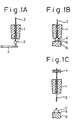
- Figs. 1A to 1C show the method for forming a bump by simply pulling a wire;
- Figs. 2A, 2B,2B' and 2C show the method for forming a bump by pulling a notched wire;
- Fig. 3 is an enlarged view of the bump portion in Fig. 1C;
- Fig. 4 is an enlarged view of the notch portion in Fig. 2B'; and
- Fig. 5 shows a semiconductor device in which wire bonding is made.
-
- The gold alloy wire of the present invention is characterized by having a composition in which prescribed amounts of Pd and Bi (hereinafter referred to as "the first group of elements"), preferably together with a prescribed amount of at least one element of Y, La, Ca and Be (hereinafter referred to as "the second group of elements") are added to a high purity gold.
- The high purity gold used in the present invention is a high purity gold having a purity of at least 99.99% by weight, preferably at least 99.995% by weight, particularly at least 99.999% by weight.
- 1) By adding Pd and Bi in the amounts specified in accordance with the present invention to the above high purity gold, an synergistic effect is obtained such that a high temperature bond strength may be maintained high and the length of a simple pull-derived tail may be stably made short. Addition of Pd in the co-presence of Bi provides an excellent effect in that a high temperature bond strength may be maintained high and the length of a simple pull-derived tail may be made uniformly short. If the content of Pd is less than 0.2% by weight, the high temperature bond strength is lower than and the length of the simple pull-derived tail is longer than those obtainable when the content of Pd is 0.2% by weight or more, even if said prescribed amount of Bi is co-present. If the content of Pd is more than 5.0% by weight, the length of the simple pull-derived tail is longer than that obtainable when the content of Pd is 5.0% by weight or less, even if said prescribed amount of Bi is co-present. Therefore, the content of Pd is specified to 0.2 to 5.0% by weight in co-presence of the prescribed content of Bi.Addition of Bi in the co-presence of Pd provides an excellent effect in that a high temperature bond strength may be kept high and the length of a simple pull-derived tail may be made uniformly short. If the content of Bi is less than 1 ppm by weight, the length of the simple pull-derived tail is longer and less uniform than that obtainable when the content of Bi is 1 ppm by weight or more, even if said prescribed amount of Pd is co-present. If the content of Bi is more than 100 ppm by weight, even if said prescribed amount of Pd is co-present, pinholes appear on the surface of the ball, at a stage of forming the ball before forming the bump, more frequently than when the content of Bi is 100 ppm by weight or less. Therefore, the content of Bi is specified to 1 to 100 ppm by weight in co-presence of the prescribed content of Pd. A preferable content of Bi in co-presence of the prescribed content of Pd is 1 to 40 ppm by weight.Thus, in accordance with the present invention, the effects of maintaining a high temperature bond strength and stably forming a short simple pull-derived tail can be obtained.
- 2) The above effects are basically obtainable in the above alloy wire even if other elements are further added to the alloy wire. Generally, the above effects obtained by adding the prescribed amounts of Pd and Bi are not lost if the total content of the elements other than Pd and Bi added to the wire is not more than 250 ppm by weight. Thus, the effects of the present invention is generally maintained even if additional elements other than Pd and Bi are added, but particularly if at least one of Y, La, Ca and Be is added in an amount in a range of 3 to 250 ppm by weight, the effect of stably obtaining a short simple pull-derived tail is equivalent and the effect of obtaining a high temperature bond strength is improved. This additional effect may be obtained by adding any one of Y, La, Ca and Be and therefore each one Of these elements is a preferable additive element. More preferably, at least three elements of these four elements are added. Most preferably, at least three elements including Y, La and Ca are added in which case the effect of a high temperature bond strength is then improved further. A preferable amount of the at least one element of the second group is 3 to 70 ppm by weight.Here, even if one or more element of the second group is added to the wire but the prescribed amounts of the elements of the first group are not added, the simple pull-derived tail length and the high temperature bond strength are improved. However, if the one or more element of the second group is added to the gold alloy wire in the presence of the prescribed amounts of the elements of the first group, the length and uniformity of the simple pull-derived tail and the high temperature bond strength are more excellent. If the one or more element of the second group is added and the prescribed amount of Bi from the first group elements is added but the prescribed amount of Pd from the first group elements is not added, the effects of improving a high temperature bond strength and a short simple pull-derived tail length are not sufficient. Accordingly, the prescribed amount of Pd should be co-present if the prescribed amount of Bi is added. Thus, in accordance with the present invention, it is stated that the element(s) of the second group, i.e., at least one of Y, La, Ca and Be should be co-present with the prescribed amounts of Pd and Bi and the amount thereof should be in an amount of 3 to 250 ppm by weight, preferably 3 to 70 ppm by weight.It should be noted that the gold alloy wire of the present invention may consist of 0.2 to 5.0% by weight of palladium (Pd) and 1 to 100 ppm by weight of bismuth (Bi), and further preferably 3 to 250 ppm by weight of at least one element selected from the group consisting of yttrium (Y), lanthanum (La), calcium (Ca) and beryllium (Be), with the remainder being gold and inevitable impurities.In accordance with the present invention, a method for forming a bump using the gold alloy wire as described above is also provided.
- 3) Simple pulling method
The simple pulling method is described with
reference to Figs. 1A to 1C.As shown in Fig. 1A, the gold alloy wire of the
present invention 2 is passed through a capillary 1, anelectric torch 3 faces an end of thewire 2 and an electric discharge is effected between theelectric torch 3 and the end of thewire 2 to heat the end of the wire and form a fused ball 4.As shown in Fig. 1B, the capillary 1 is lowered to press and bond the ball to theelectrode 5 on anIC chip 6. Although not shown in the figure, since ultrasound is simultaneously applied to theball 4 through the capillary 1 and theIC chip 6 is heated by a heater block, theball 4 is thermally bonded so that theball 4 is deformed into a two-stepflat shape 4'.As shown in Fig. 1C, the capillary 1 is pulled upward while theclamper 7 holds thegold alloy wire 2. As a result, thewire 2 is broken and separated from the deformed ball 4' to leave a bump 4', i.e., the ball pressed and bonded to theelectrode 5 of the IC chip 6.After that, the top of the bump 4' is connected to an outer terminal (not shown).Here, as shown in Fig. 1C, a wire portion remains on the top of the bump 4'. Fig. 3 is an enlarged figure of this bump 4'. The tail length used in the present invention is referred to the length L of the wire piece 8 remaining on thebump 4'.When a bump is formed by this simple pulling method and the gold alloy wire is used in accordance with the present invention, the length of the tail (the simple pull-derived tail) can be uniformly short. - 4) Notched pulling method
-
- The notched pulling method is described with reference to Figs. 2A, 2B, 2B' and 2C.
- As shown in Figs. 2A and 2B, a
ball 4 is pressed and bonded to theelectrode 5 on theIC chip 6 and deformed into the two-step flat or mount shape, in the same manner as described before with reference to Figs. 1A and 1B. - As shown in Fig. 2B', a sharp edge of a notch-forming
jig 7 approaches, from the side, thegold alloy wire 2 at a desired location above the two-step flat or mount shape 4' to form a notch or recess. Fig. 4 is an enlarged figure of this stage, in which a notch orrecess 9 is shown. The shape of the notch orrecess 9 is not limited to a v-shape. - Then as shown in Fig. 2C, the
wire 2 is pulled upward in the same manner as in Fig. 1C, so that thewire 2 is broken or cut from the bonded ball 4' and a bump 4' on theelectrode 5 of theIC chip 6 is thus formed. - The top of the bump 4' is then connected to an outer terminal, although it is not shown.
- In this case, a wire piece 8 is left on the bump 4'.
- This notched pulling method is preferable since the tail length may be controlled to a desired length by setting the location of the notch.
- An electrically conductive material may be used for connecting the bump 4' with the outer terminal.
- A mixture of a high purity gold having a purity of 99.999% by weight with prescribed amounts of Pd and Bi was melted in a vacuum furnace and cast to obtain a gold alloy ingot having a composition as shown in Table 1, that is, 0.2% by weight of Pd and 20 ppm by weight of Bi. The ingot was cold worked by a groove roller drawing machine and intermediately annealed to obtain a final wire diameter of 25 µm. The wire was finally annealed to have an elongation of 2 to 3%.
- This gold alloy wire was bonded onto electrodes of an IC chip with a wire bonding machine by an ultrasound thermal pressing bonding method in the manner as shown in Figs. 1A to 1C. The bonded wires were then simply pulled upward to form ten bumps.
- The obtained bumps were examined by measuring the tail length and carrying out a high temperature bond test followed by observation of the appearance of the bump or ball. The results are shown in Table 1.
- The same procedures and examinations as in Example 1 were conducted except that the compositions of the wire were made as shown in Tables 1 to 3.
- The tail length of ten samples for each of Examples and Comparative Examples was measured by a length-measuring microscope. The average length and standard deviation were calculated.
- Ten samples for each of Examples and Comparative Examples were placed in a thermostatic furnace set to 300°C for 500 hours, followed by measuring the shearing strength by a shearing strength measuring machine. The average value of the shearing strength was taken as the high temperature bond strength.
- The appearance of the ball when it was formed was observed by a microscope to determine if there were pinholes on the outer surface of the ball. When pinholes were seen, the result was considered bad. When no pinhole was seen, the result was considered good. In Tables, "good" is shown by o, and "bad" is shown as ×.
-
- 1) In Examples 1 to 6 in which the prescribed
amounts of Pd and Bi (first group of elements) were added
to the gold, the following excellent results were
obtained.
- i) The average tail length was in a range of 33.4 to 39.6 µm, and the standard deviation of the tail length which expresses the non-uniformity of the tail length was in a range of 5.0 to 8.8 µm. The length of the tail was short and uniform.
- ii) The high temperature bond strength was as high as in a range of 0.413 to 0.551 N (42.1 - 56.2 gf).
- iii) Pinholes were not observed in any Examples.
- 2) In Examples 7 to 41 in which the prescribed
amount(s) of at least one of Y, La, Ca and Be (second
group of elements) in addition to the prescribed amounts
of Pd and Bi (first group of elements) were added to the
gold, the following excellent effects were exhibited.
Particularly, the high temperature bond strength was more
excellent than in the case of addition of only the first
group of element(s).
- i) The average tail length was in a range of 31.1 to 37.6 µm, and the standard deviation of the tail length which expresses the non-uniformity of the tail length was in a range of 4.4 to 9.9 µm. The length of the tail was short and uniform.
- ii) The high temperature bond strength was as high as in a range of 0.420 to 0.661 N (42.8 - 67.4 gf).
- iii) The high temperature bond strength was
further improved by adding the element(s) of the second
group.
- a) When comparing Example 1 with Examples 7, 13 and 19 in which the element(s) of the second group was/were further added to Example 1, the high temperature bond strength was improved from 0.413 N (42.1 gf) to a range of 0.420 to 0.425 N (42.8 - 43.3 gf).
- b) When comparing Examples 2 to 6 with corresponding Examples in which the element(s) of the second group was/were further added to Examples 2 to 6, the high temperature bond strength was similarly improved.
- iv) Pinholes were not observed in any Examples.
- v) In Examples 40 to 41 in which three or more elements of the second group were added, the high temperature bond strength was the most excellent, as 0.659 to 0.661 N (67.2 - 67.4 gf).
- 3) In Comparative Example 1 in which either of the elements of the first or of second groups were not added, the average tail length was 75.2 µm, and the standard deviation of the tail length was 32.3 µm. The high temperature bond strength was 0.051 N (5.2 gf). These results were bad.
- 4) In Comparative Examples 2, 3, 7 and 8 in which the prescribed amount of Bi was added and Pd was added in an amount less than 0.2% by weight, the average tail length was 46.0 to 50.9 µm, the standard deviation of the tail length was 8.3 to 12.7 µm, and the high temperature bond strength was 0.132 to 0.161 N (13.5 - 16.4 gf). These results were bad.
- 5) In Comparative Example 4 in which the prescribed amount of Bi was added and Pd was added in an amount beyond 5.0% by weight, the average tail length was 58.9 µm, and the standard deviation of the tail length was 14.4 µm. These results were bad.
- 6) In Comparative Examples 5 and 9 in which the prescribed amount of Pd was added and Bi was not added, the standard deviation of the tail length was bad at 19.5 to 21.4 µm. The high temperature bond strength was 0.326 to 0.361 N (33.2 - 36.8 gf), improved in comparison with Comparative Example 1, but inferior to Examples of the present invention.
- 7) In Comparative Example 6 in which the
prescribed amount of Pd was added and Bi was added in an
amount beyond 100 ppm by weight, pinholes were observed.
The high temperature bond strength was low and the
deviation was large and, therefore, the numerical·values
thereof are not shown in Tables.


-
- In accordance with the present invention, a novel gold alloy wire in which the prescribed amounts of Pd and Bi are added, especially suitable for forming a bump to an IC chip, is provided and the following effects are obtained.
- 1) The simple pull-derived tail can be stably formed with a short length. As a result, bumps can be stably formed by the simple pulling method and the reliability of a semiconductor device is advantageously improved.
- 2) The high temperature bond strength can be improved which is advantageous in increasing the reliability of a semiconductor device. If the prescribed amount of at least one of Y, La, Ca and Be is further added, the high temperature bond strength can be further improved which is further advantageous in increasing the reliability of a semiconductor device.
-
- Further, by forming a bump using the above gold alloy wire and the simple pulling method,
- 1) a gold bump having a uniform tail length can be stably formed by a simple pulling operation, which is advantageous in improvement in the productivity, and
- 2) the high temperature bond strength can be improved which is advantageous in increasing the reliability of a semiconductor device.
-
- Further, by forming a bump using the above gold alloy wire and the notched pulling method,
- 1) the tail length can be set to a desired length and therefore the tail length can be made more uniformly short, and
- 2) the high temperature bond strength can be improved which is advantageous in increasing the reliability of a semiconductor device.
-
- A mixture of a high purity gold having a purity of 99.999% by weight with prescribed amounts of Pd and Bi was melted in a vacuum furnace and cast to obtain a gold alloy ingot having a composition as shown in Table 4, that is, 1.0% by weight of Pd and 30 ppm by weight of Bi. The ingot was cold worked by a groove roller drawing machine and intermediately annealed to obtain a final wire diameter of 30 µm. The wire was finally annealed to have an elongation of 4%.
- Using an automatic wire bonder (UTC-50 type, Shinkawa K.K.), wire bonding was conducted to bond between 100 aluminum electrodes of an IC chip and lead frames with the above obtained gold alloy wire by a ultrasound and heat pressing bonding method.
- The loop height of the above sample was measured using a measuring microscope (STM-MJS type, Olympus K.K.). The loop height was the height H from the top surface of the
IC chip 11 to the highest point of the loop as shown in Fig. 4. 100 samples were measured for each Example and the average of the loop heights of the 100 samples was used as the loop height in Table 4. - Also, several hundreds samples for each Example were placed at 200°C for 500 hours and the shearing strength was measured using a shear tester. The average of 50 samples was used as the high temperature bond strength in Table 4.
Composition Results wt% wt ppm Loop height (µm) High temperature bond strength (N) Pd Bi Y La Ca Be Au Ex. 42 1.0 30 - - - - remainder 84 0.657 Ex. 43 1.0 1 - - - - remainder 110 0.598 Ex. 44 1.0 30 50 - - - remainder 88 0.667 Ex. 45 1.0 30 - 50 - - remainder 87 0.667 Ex. 46 1.0 30 - - 50 - remainder 92 0.637 Ex. 47 1.0 30 20 - - 10 remainder 90 0.667 - It is noted that when conventional gold alloy wires are used, the loop height is typically more than about 170 µm and the high temperature bond strength is typically less than about 0.294 N (30 gf).
- Thus, when a gold alloy wire of the present invention is used, the loop height can be substantially reduced and the high temperature bonding strength can be improved.
Claims (22)
- A gold alloy wire comprising 0,2 to 5,0% by weight of palladium (Pd) and 1 to 100 ppm by weight of bismuth (Bi), optionally with 3 to 250 ppm by weight of at least one element selected from the group consisting of yttrium (Y), lanthanum (La), calcium (Ca) and beryllium (Be), the remainder being gold (Au) and inevitable impurities.
- The gold alloy wire according to claim 1 wherein the total amount of the impurities is less than 0.001% by weight.
- The gold alloy wire according to claim 1 wherein said amount of Pd is in a range of 0,5 to 5,0% by weight.
- The gold alloy wire according to claim 1 wherein said amount of Bi is in a range of 1 to 40 ppm by weight.
- The gold alloy wire according to claim 1 wherein said at least one element selected from the group consisting of yttrium (Y), lanthanum (La), calcium (Ca) and beryllium (Be) is contained in said gold alloy wire.
- The gold alloy wire according to claim 5 wherein said amount of said at least one element is 3 to 70 ppm by weight.
- The gold alloy wire according to claim 5 wherein at least three elements selected from the group consisting of yttrium (Y), lanthanum (La), calcium (Ca) and beryllium (Be) are added to said gold.
- The gold alloy wire according to claim 5 wherein at least three elements of yttrium (Y), lanthanum (La) and calcium (Ca) are added to said gold.
- The gold alloy wire according to claim 1 wherein said wire is especially adapted for forming a bump.
- The gold alloy wire according to claim 1 wherein said wire is especially adapted for wire bonding.
- A method for forming a gold alloy bump, comprising the steps of: forming a ball at an end of a gold alloy wire passing through a capillary, lowering said capillary to press and bond said ball to an electrode of an IC chip, and pulling said gold alloy wire upward to break said gold alloy wire from said ball bonded to said electrode, to thereby form a gold alloy bump on said electrode of said IC chip, wherein said gold alloy wire comprises 0,2 to 5,0% by weight of palladium (Pd) and 1 to 100 ppm by weight of bismuth (Bi), optionally with 3 to 250 ppm by weight of at least one element selected from the group consisting of yttrium (Y), lanthanum (La), calcium (Ca) and beryllium (Be), the remainder being gold (Au) and inevitable impurities.
- The method according to claim 11 wherein the total amount of the impurities is less than 0.001% by weight.
- The method according to claim 11 wherein said amount of Pd is in a range of 0,5 to 5,0% by weight.
- The method according to claim 11 wherein at least one element selected from the group consisting of yttrium (Y), lanthanum (La), calcium (Ca) and beryllium (Be) in a an amount of 3 to 250 ppm by weight is further added to said gold.
- The method according to claim 14 wherein at least three elements of yttrium (Y), lanthanum (La) and calcium (Ca) are added to said gold.
- A method for forming a gold alloy bump comprising the steps of: forming a ball at an end of a gold alloy wire passing through a capillary, lowering said capillary to press and bond said ball to an electrode of an IC chip, making a notch to said gold alloy wire above said ball, and pulling said gold alloy wire upward to break said gold alloy wire from said ball bonded to said electrode, to thereby form a gold alloy bump on said electrode of said IC chip, wherein said gold alloy wire comprises 0,2 to 5,0% by weight of palladium (Pd) and 1 to 100 ppm by weight of bismuth (Bi), optionally with 3 to 250 ppm by weight of at least one element selected from the group consisting of yttrium (Y), lanthanum (La), calcium (Ca) and beryllium (Be), the remainder being gold (Au) and inevitable impurities.
- The method according to claim 16 wherein the total amount of the impurities is less than 0.001% by weight.
- The method according to claim 16 wherein said amount of Pd is in a range of 0,5 to 5,0% by weight.
- The method according to claim 16 wherein at least one element selected from the group consisting of yttrium (Y), lanthanum (La), calcium (Ca) and beryllium (Be) in an amount of 3 to 250 ppm by weight is further added to said gold.
- The method according to claim 19 wherein at least three elements of yttrium (Y), lanthanum (La) and calcium (Ca) are added to said gold.
- A method for wire bonding wherein a wire used comprises 0,2 to 5,0% by weight of palladium (Pd) and 1 to 100 ppm by weight of bismuth (Bi), optionally with 3 to 250 ppm by weight of at least one element selected from the group consisting of yttrium (Y), lanthanum (La), calcium (Ca) and beryllium (Be), the remainder being gold (Au) and inevitable impurities.
- The methods according to claim 21 wherein said at least one element selected from the group consisting of yttrium (Y), lanthanum (La), calcium (Ca) and beryllium (Be) is contained in said gold alloy wire.
Applications Claiming Priority (3)
| Application Number | Priority Date | Filing Date | Title |
|---|---|---|---|
| JP13354696A JP3328135B2 (en) | 1996-05-28 | 1996-05-28 | Gold alloy wire for bump formation and bump formation method |
| JP133546/96 | 1996-05-28 | ||
| JP13354696 | 1996-05-28 |
Publications (2)
| Publication Number | Publication Date |
|---|---|
| EP0810293A1 EP0810293A1 (en) | 1997-12-03 |
| EP0810293B1 true EP0810293B1 (en) | 2001-10-24 |
Family
ID=15107346
Family Applications (1)
| Application Number | Title | Priority Date | Filing Date |
|---|---|---|---|
| EP97250166A Expired - Lifetime EP0810293B1 (en) | 1996-05-28 | 1997-05-28 | Gold alloy wire and method for making a bump |
Country Status (8)
| Country | Link |
|---|---|
| US (2) | US6159420A (en) |
| EP (1) | EP0810293B1 (en) |
| JP (1) | JP3328135B2 (en) |
| KR (1) | KR100275001B1 (en) |
| CN (1) | CN1065001C (en) |
| DE (1) | DE69707559T2 (en) |
| MY (1) | MY120121A (en) |
| TW (1) | TW327697B (en) |
Cited By (2)
| Publication number | Priority date | Publication date | Assignee | Title |
|---|---|---|---|---|
| SG90251A1 (en) * | 2000-05-31 | 2002-07-23 | Tanaka Electronics Ind | Gold wire for semiconductor element connection and semiconductor element connection method |
| US6467677B1 (en) | 1998-03-04 | 2002-10-22 | Robert Bosch Gmbh | Method and contact point for producing an electrical connection |
Families Citing this family (15)
| Publication number | Priority date | Publication date | Assignee | Title |
|---|---|---|---|---|
| US6523255B2 (en) * | 2001-06-21 | 2003-02-25 | International Business Machines Corporation | Process and structure to repair damaged probes mounted on a space transformer |
| US6500760B1 (en) | 2001-08-02 | 2002-12-31 | Sandia Corporation | Gold-based electrical interconnections for microelectronic devices |
| US6858943B1 (en) | 2003-03-25 | 2005-02-22 | Sandia Corporation | Release resistant electrical interconnections for MEMS devices |
| KR100899322B1 (en) * | 2004-09-30 | 2009-05-27 | 타나카 덴시 코오교오 카부시키가이샤 | Au ALLOY BONDING WIRE |
| KR101002062B1 (en) * | 2004-09-30 | 2010-12-17 | 타나카 덴시 코오교오 카부시키가이샤 | Wire bump |
| WO2006057230A1 (en) * | 2004-11-26 | 2006-06-01 | Tanaka Denshi Kogyo K.K. | Au BONDING WIRE FOR SEMICONDUCTOR ELEMENT |
| US7595560B2 (en) * | 2005-02-22 | 2009-09-29 | Nec Electronics Corporation | Semiconductor device |
| US8174119B2 (en) | 2006-11-10 | 2012-05-08 | Stats Chippac, Ltd. | Semiconductor package with embedded die |
| US8133762B2 (en) | 2009-03-17 | 2012-03-13 | Stats Chippac, Ltd. | Semiconductor device and method of providing z-interconnect conductive pillars with inner polymer core |
| US8193034B2 (en) | 2006-11-10 | 2012-06-05 | Stats Chippac, Ltd. | Semiconductor device and method of forming vertical interconnect structure using stud bumps |
| JP4195495B1 (en) * | 2007-11-06 | 2008-12-10 | 田中電子工業株式会社 | Gold alloy wire for ball bonding |
| JP2010123817A (en) * | 2008-11-21 | 2010-06-03 | Fujitsu Ltd | Wire bonding method, electronic apparatus, and method of manufacturing the same |
| US8540136B1 (en) | 2012-09-06 | 2013-09-24 | Taiwan Semiconductor Manufacturing Company, Ltd. | Methods for stud bump formation and apparatus for performing the same |
| TWI685391B (en) * | 2016-03-03 | 2020-02-21 | 美商史達克公司 | Three-dimensional parts and methods fabricating the same |
| CN116329830B (en) * | 2023-05-29 | 2023-08-29 | 宁波尚进自动化科技有限公司 | Welding method of chip pins |
Family Cites Families (31)
| Publication number | Priority date | Publication date | Assignee | Title |
|---|---|---|---|---|
| JPS5649535A (en) * | 1979-09-28 | 1981-05-06 | Tanaka Kikinzoku Kogyo Kk | Bonding wire for semiconductor device |
| US4330329A (en) * | 1979-11-28 | 1982-05-18 | Tanaka Denshi Kogyo Kabushiki Kaisha | Gold bonding wire for semiconductor elements and the semiconductor element |
| GB2116208B (en) * | 1981-12-04 | 1985-12-04 | Mitsubishi Metal Corp | Fine gold alloy wire for bonding of a semiconductor device |
| JPS6152961A (en) * | 1984-08-22 | 1986-03-15 | Sumitomo Electric Ind Ltd | Production of gold alloy wire |
| US4702302A (en) * | 1983-02-23 | 1987-10-27 | Sumitomo Electric Industries Ltd. | Method of making thin alloy wire |
| JPS59208751A (en) * | 1983-05-13 | 1984-11-27 | Hitachi Ltd | Formation of bump |
| US5476211A (en) * | 1993-11-16 | 1995-12-19 | Form Factor, Inc. | Method of manufacturing electrical contacts, using a sacrificial member |
| US5917707A (en) * | 1993-11-16 | 1999-06-29 | Formfactor, Inc. | Flexible contact structure with an electrically conductive shell |
| JPS62152143A (en) * | 1985-12-26 | 1987-07-07 | Toshiba Corp | Formation of bump |
| JPS63145729A (en) * | 1986-03-28 | 1988-06-17 | Nittetsu Micro Metal:Kk | Gold wire for bonding semiconductor device |
| JP2737953B2 (en) * | 1988-09-29 | 1998-04-08 | 三菱マテリアル株式会社 | Gold alloy wire for gold bump |
| JPH02152143A (en) | 1988-12-02 | 1990-06-12 | Toshiba Corp | X-ray image tube and its manufacture |
| GB2231336B (en) * | 1989-04-28 | 1993-09-22 | Tanaka Electronics Ind | Gold wire for the bonding of a semiconductor device |
| US5139883A (en) * | 1989-05-09 | 1992-08-18 | Grigory Raykhtsaum | Intermetallic time-temperature integration fuse |
| JPH03145729A (en) | 1989-10-31 | 1991-06-20 | Sony Corp | Manufacture of semiconductor device |
| JPH082623B2 (en) | 1990-08-23 | 1996-01-17 | ソマール株式会社 | Ultra high molecular weight polyethylene composite sheet and method for producing the same |
| JP3145729B2 (en) | 1991-05-28 | 2001-03-12 | チノン株式会社 | Multi-point distance measuring device |
| JP3090549B2 (en) * | 1992-09-30 | 2000-09-25 | 田中電子工業株式会社 | Bonding wire for semiconductor device |
| JP3064692B2 (en) * | 1992-09-30 | 2000-07-12 | 田中電子工業株式会社 | Bonding wire for semiconductor device |
| JPH06112251A (en) * | 1992-09-30 | 1994-04-22 | Tanaka Denshi Kogyo Kk | Bonding wire for semiconductor element |
| JP2780611B2 (en) * | 1993-09-06 | 1998-07-30 | 三菱マテリアル株式会社 | Gold decorative materials hardened by alloying small amounts of components |
| JP3221179B2 (en) * | 1993-09-06 | 2001-10-22 | 三菱マテリアル株式会社 | High hardness wire drawn wire for gold ornaments with excellent hardness stability |
| US5884398A (en) * | 1993-11-16 | 1999-03-23 | Form Factor, Inc. | Mounting spring elements on semiconductor devices |
| JP3085090B2 (en) * | 1994-06-07 | 2000-09-04 | 住友金属鉱山株式会社 | Bonding wire |
| JPH08109424A (en) * | 1994-08-18 | 1996-04-30 | Tanaka Denshi Kogyo Kk | Gold wire for bonding |
| JPH08127828A (en) * | 1994-10-28 | 1996-05-21 | Tanaka Denshi Kogyo Kk | Gold wire for bonding |
| JPH08193233A (en) * | 1995-01-12 | 1996-07-30 | Mitsubishi Materials Corp | Gold alloy fine wire for semiconductor device |
| JPH08325657A (en) * | 1995-05-26 | 1996-12-10 | Tanaka Denshi Kogyo Kk | Gold wire for bonding |
| JP3585993B2 (en) * | 1995-05-26 | 2004-11-10 | 田中電子工業株式会社 | Gold wire for bonding |
| JP3367544B2 (en) * | 1995-08-23 | 2003-01-14 | 田中電子工業株式会社 | Gold alloy fine wire for bonding and method of manufacturing the same |
| JP3222054B2 (en) | 1996-02-06 | 2001-10-22 | 信越化学工業株式会社 | Rubber composition |
-
1996
- 1996-05-28 JP JP13354696A patent/JP3328135B2/en not_active Expired - Lifetime
-
1997
- 1997-05-23 US US08/863,034 patent/US6159420A/en not_active Expired - Lifetime
- 1997-05-27 KR KR1019970020964A patent/KR100275001B1/en not_active Expired - Fee Related
- 1997-05-27 TW TW086107139A patent/TW327697B/en not_active IP Right Cessation
- 1997-05-28 MY MYPI97002327A patent/MY120121A/en unknown
- 1997-05-28 EP EP97250166A patent/EP0810293B1/en not_active Expired - Lifetime
- 1997-05-28 CN CN971135681A patent/CN1065001C/en not_active Expired - Lifetime
- 1997-05-28 DE DE69707559T patent/DE69707559T2/en not_active Expired - Lifetime
-
1999
- 1999-01-05 US US09/226,033 patent/US6213382B1/en not_active Expired - Lifetime
Cited By (3)
| Publication number | Priority date | Publication date | Assignee | Title |
|---|---|---|---|---|
| US6467677B1 (en) | 1998-03-04 | 2002-10-22 | Robert Bosch Gmbh | Method and contact point for producing an electrical connection |
| SG90251A1 (en) * | 2000-05-31 | 2002-07-23 | Tanaka Electronics Ind | Gold wire for semiconductor element connection and semiconductor element connection method |
| US6492593B2 (en) | 2000-05-31 | 2002-12-10 | Tanaka Denshi Kogyo K.K. | Gold wire for semiconductor element connection and semiconductor element connection method |
Also Published As
| Publication number | Publication date |
|---|---|
| DE69707559T2 (en) | 2002-05-16 |
| JPH09321076A (en) | 1997-12-12 |
| TW327697B (en) | 1998-03-01 |
| US6159420A (en) | 2000-12-12 |
| EP0810293A1 (en) | 1997-12-03 |
| US6213382B1 (en) | 2001-04-10 |
| KR970077400A (en) | 1997-12-12 |
| MY120121A (en) | 2005-09-30 |
| KR100275001B1 (en) | 2001-01-15 |
| CN1173546A (en) | 1998-02-18 |
| CN1065001C (en) | 2001-04-25 |
| JP3328135B2 (en) | 2002-09-24 |
| DE69707559D1 (en) | 2001-11-29 |
Similar Documents
| Publication | Publication Date | Title |
|---|---|---|
| US6159420A (en) | Gold alloy wire and method for making a bump | |
| KR100294242B1 (en) | Alloy alloy wire for wedge bonding and use of the wire in wedge bonding | |
| KR101536554B1 (en) | Bonding wire | |
| EP1160344B1 (en) | Gold wire for semiconductor element connection and semiconductor element connection method | |
| JPH1145899A (en) | Bonding wire | |
| JP3690902B2 (en) | Gold alloy wire for wedge bonding | |
| EP1168439B1 (en) | Gold bond wire for a semiconductor device | |
| JPH11126788A (en) | Gold alloy wire for IC chip connection | |
| JPH1098063A (en) | Gold alloy wire for wedge bonding | |
| JP3615901B2 (en) | Gold alloy wire for semiconductor element bonding | |
| JP3085090B2 (en) | Bonding wire | |
| JP2773202B2 (en) | Au alloy extra fine wire for semiconductor element bonding | |
| JP3358295B2 (en) | Bonding wire | |
| JP3586909B2 (en) | Bonding wire | |
| JP3669810B2 (en) | Gold alloy wire for semiconductor element bonding | |
| JP3744131B2 (en) | Bonding wire | |
| JPH104114A (en) | Bonding wire | |
| JPH07305126A (en) | Gold alloy wire for bonding | |
| JPH11340264A (en) | Gold alloy wire for wire bump formation and wire bump formation method | |
| JPH10233411A (en) | Gold alloy wire for semiconductor element bonding | |
| KR20030096985A (en) | Gold alloy wire for bonding of semiconductor device | |
| JPH10303238A (en) | Gold alloy wire for bonding on semiconductor device | |
| JPH0448734A (en) | Aluminum alloy for bump |
Legal Events
| Date | Code | Title | Description |
|---|---|---|---|
| PUAI | Public reference made under article 153(3) epc to a published international application that has entered the european phase |
Free format text: ORIGINAL CODE: 0009012 |
|
| AK | Designated contracting states |
Kind code of ref document: A1 Designated state(s): DE FR GB NL |
|
| 17P | Request for examination filed |
Effective date: 19971026 |
|
| 17Q | First examination report despatched |
Effective date: 19990201 |
|
| GRAG | Despatch of communication of intention to grant |
Free format text: ORIGINAL CODE: EPIDOS AGRA |
|
| GRAG | Despatch of communication of intention to grant |
Free format text: ORIGINAL CODE: EPIDOS AGRA |
|
| GRAH | Despatch of communication of intention to grant a patent |
Free format text: ORIGINAL CODE: EPIDOS IGRA |
|
| GRAH | Despatch of communication of intention to grant a patent |
Free format text: ORIGINAL CODE: EPIDOS IGRA |
|
| GRAA | (expected) grant |
Free format text: ORIGINAL CODE: 0009210 |
|
| AK | Designated contracting states |
Kind code of ref document: B1 Designated state(s): DE FR GB NL |
|
| REF | Corresponds to: |
Ref document number: 69707559 Country of ref document: DE Date of ref document: 20011129 |
|
| REG | Reference to a national code |
Ref country code: GB Ref legal event code: IF02 |
|
| ET | Fr: translation filed | ||
| PLBE | No opposition filed within time limit |
Free format text: ORIGINAL CODE: 0009261 |
|
| STAA | Information on the status of an ep patent application or granted ep patent |
Free format text: STATUS: NO OPPOSITION FILED WITHIN TIME LIMIT |
|
| 26N | No opposition filed | ||
| PGFP | Annual fee paid to national office [announced via postgrant information from national office to epo] |
Ref country code: GB Payment date: 20100329 Year of fee payment: 14 |
|
| PGFP | Annual fee paid to national office [announced via postgrant information from national office to epo] |
Ref country code: FR Payment date: 20100525 Year of fee payment: 14 |
|
| PGFP | Annual fee paid to national office [announced via postgrant information from national office to epo] |
Ref country code: NL Payment date: 20100518 Year of fee payment: 14 Ref country code: DE Payment date: 20100526 Year of fee payment: 14 |
|
| REG | Reference to a national code |
Ref country code: DE Ref legal event code: R119 Ref document number: 69707559 Country of ref document: DE |
|
| REG | Reference to a national code |
Ref country code: DE Ref legal event code: R119 Ref document number: 69707559 Country of ref document: DE |
|
| REG | Reference to a national code |
Ref country code: NL Ref legal event code: V1 Effective date: 20111201 |
|
| GBPC | Gb: european patent ceased through non-payment of renewal fee |
Effective date: 20110528 |
|
| PG25 | Lapsed in a contracting state [announced via postgrant information from national office to epo] |
Ref country code: NL Free format text: LAPSE BECAUSE OF NON-PAYMENT OF DUE FEES Effective date: 20111201 |
|
| REG | Reference to a national code |
Ref country code: FR Ref legal event code: ST Effective date: 20120131 |
|
| PG25 | Lapsed in a contracting state [announced via postgrant information from national office to epo] |
Ref country code: FR Free format text: LAPSE BECAUSE OF NON-PAYMENT OF DUE FEES Effective date: 20110531 |
|
| PG25 | Lapsed in a contracting state [announced via postgrant information from national office to epo] |
Ref country code: GB Free format text: LAPSE BECAUSE OF NON-PAYMENT OF DUE FEES Effective date: 20110528 |
|
| PG25 | Lapsed in a contracting state [announced via postgrant information from national office to epo] |
Ref country code: DE Free format text: LAPSE BECAUSE OF NON-PAYMENT OF DUE FEES Effective date: 20111130 |