EP0809833B1 - Procede de fabrication de cartes electroniques - Google Patents
Procede de fabrication de cartes electroniques Download PDFInfo
- Publication number
- EP0809833B1 EP0809833B1 EP96904150A EP96904150A EP0809833B1 EP 0809833 B1 EP0809833 B1 EP 0809833B1 EP 96904150 A EP96904150 A EP 96904150A EP 96904150 A EP96904150 A EP 96904150A EP 0809833 B1 EP0809833 B1 EP 0809833B1
- Authority
- EP
- European Patent Office
- Prior art keywords
- monomer
- mixture
- methacrylate
- polymer
- card
- Prior art date
- Legal status (The legal status is an assumption and is not a legal conclusion. Google has not performed a legal analysis and makes no representation as to the accuracy of the status listed.)
- Expired - Lifetime
Links
Images


Classifications
-
- G—PHYSICS
- G06—COMPUTING; CALCULATING OR COUNTING
- G06K—GRAPHICAL DATA READING; PRESENTATION OF DATA; RECORD CARRIERS; HANDLING RECORD CARRIERS
- G06K19/00—Record carriers for use with machines and with at least a part designed to carry digital markings
- G06K19/06—Record carriers for use with machines and with at least a part designed to carry digital markings characterised by the kind of the digital marking, e.g. shape, nature, code
- G06K19/067—Record carriers with conductive marks, printed circuits or semiconductor circuit elements, e.g. credit or identity cards also with resonating or responding marks without active components
- G06K19/07—Record carriers with conductive marks, printed circuits or semiconductor circuit elements, e.g. credit or identity cards also with resonating or responding marks without active components with integrated circuit chips
- G06K19/077—Constructional details, e.g. mounting of circuits in the carrier
- G06K19/07745—Mounting details of integrated circuit chips
-
- G—PHYSICS
- G06—COMPUTING; CALCULATING OR COUNTING
- G06K—GRAPHICAL DATA READING; PRESENTATION OF DATA; RECORD CARRIERS; HANDLING RECORD CARRIERS
- G06K19/00—Record carriers for use with machines and with at least a part designed to carry digital markings
- G06K19/04—Record carriers for use with machines and with at least a part designed to carry digital markings characterised by the shape
- G06K19/041—Constructional details
-
- G—PHYSICS
- G06—COMPUTING; CALCULATING OR COUNTING
- G06K—GRAPHICAL DATA READING; PRESENTATION OF DATA; RECORD CARRIERS; HANDLING RECORD CARRIERS
- G06K19/00—Record carriers for use with machines and with at least a part designed to carry digital markings
- G06K19/06—Record carriers for use with machines and with at least a part designed to carry digital markings characterised by the kind of the digital marking, e.g. shape, nature, code
- G06K19/067—Record carriers with conductive marks, printed circuits or semiconductor circuit elements, e.g. credit or identity cards also with resonating or responding marks without active components
- G06K19/07—Record carriers with conductive marks, printed circuits or semiconductor circuit elements, e.g. credit or identity cards also with resonating or responding marks without active components with integrated circuit chips
- G06K19/077—Constructional details, e.g. mounting of circuits in the carrier
- G06K19/07749—Constructional details, e.g. mounting of circuits in the carrier the record carrier being capable of non-contact communication, e.g. constructional details of the antenna of a non-contact smart card
-
- H—ELECTRICITY
- H01—ELECTRIC ELEMENTS
- H01L—SEMICONDUCTOR DEVICES NOT COVERED BY CLASS H10
- H01L2924/00—Indexing scheme for arrangements or methods for connecting or disconnecting semiconductor or solid-state bodies as covered by H01L24/00
- H01L2924/0001—Technical content checked by a classifier
- H01L2924/0002—Not covered by any one of groups H01L24/00, H01L24/00 and H01L2224/00
Definitions
- the invention relates to a method for manufacturing electronic cards as well as cards obtained by such a process.
- the word card should be considered in this invention, in a broad sense, including in particular any portable object with standardized dimensions, and comprising, on the one hand, a micromodule and, on the other apart, a body serving as a portable support.
- the invention relates in particular to smart cards and, among these cards, the cards having a functioning contactless, in which the micromodule is connected to an antenna for electromagnetic transmission Datas.
- contactless card a card with functioning exclusively contactless, or a hybrid card having contactless operation and a conventional operation, with contacts.
- the manufacture of electronic cards in large series can be carried out by different methods.
- Certain methods involve injection, at a temperature above 90 ° C. and under high pressure, for example of the order of 700 kg / cm 2 , of a viscous thermoplastic material polymerized in the molten state in a closed cavity d 'a mold. After cooling below its melting point, this material forms a thickness of the card body.
- EP-A-0570784 describes a process for the manufacture of a contactless type smart card, which spreads on a work plan a binder in liquid form and preferably with sufficient viscosity so as not to spread so too important.
- An electronic module is embedded in the layer formed by said binder.
- the object of the present invention is to provide a process for manufacturing electronic cards in large series, which overcomes the costs at a lower cost aforementioned drawbacks, and which allows in particular a simple adjustment of the viscosity of the plastic injected or dispensed.
- Another object of the invention is to allow obtaining card thicknesses whose characteristics, such as adhesion, stiffness or temperature resistance are adjustable and controllable with ease.
- the subject of the invention is therefore a method of manufacture of an electronic card as defined in claim 1.
- the electronic cards 1 correspond to ISO standard 7810. They include a micromodule 2 and a body of map 3.
- the card body 3 is a parallelepiped thin rectangle with dimensions outside all are of the order of 85 mm in length, 54 mm in width, and 0.76 mm thick. It has n overlapping layers. The number n can be equal to one. However, in the general case, it is greater than one. In the example of FIGS. 1A and 1B, it is equal to three, and the card body 3 then comprises a layer top 4, bottom layer 5, and underlay 6.
- Micromodule 2 is inserted in the card body 3. It is in contact with a plastic layer of the card body 3, for example the underlay 6. It has an integrated circuit chip 7 and connection terminals 8.
- connection terminals 8 are connected to pads contact 9 metallic flush with the surface of the card body 3 and forming metallizations 10.
- connection terminals 8 are connected to pads contact 11 of an antenna 12 included in the body of card 3.
- the antenna 12 is formed either of a coil of metal wire with a diameter of around 30 ⁇ m, either of a metallized or laminated dielectric with metal around 80 ⁇ m thick, or, in the case of a microwave antenna, a dielectric sheet the thickness of which is close to 80 ⁇ m.
- a mixture comprising at least one monomer referenced 100 in Figure 2.
- This monomer 100 is liquid and of low viscosity.
- the viscosity of the monomers 100 is between 100 and 1,000 mPa.s approximately and preferably less than 500 mPa.s about at a Trep temperature. spreading the mixed.
- initiator 101 can be a catalyst ionic or radical, or so, radiation actinic.
- the initiator 101 is a catalyst, it is present in the mixture during spreading, and decomposes during the priming of the polymerization, into one or more products of decomposition 102 of said priming.
- the initiator 101 is a actinic radiation such as, for example, a UV radiation
- said initiator 101 is, of course, not present in the mixture but it induces the decomposition of an agent thereof which forms a radical or ion initiating polymerization.
- the decomposition products 102 of said initiation there are one or more decomposition products 102 of said initiation.
- the polymerization time is important, greater than 15 about minutes. Also, we accelerate the reaction of polymerization by adding, to the mixture comprising initiator 101 and monomer 100, accelerator 103 who cannot, alone, initiate the reaction of polymerization.
- the quantity is adjusted accelerator 103 so as to adjust, in particular, the polymerization rate of monomer 100. More the accelerator 103 is present in large quantities in mixing and active, the faster the polymerization, and the more profitable the process is industrially.
- the polymerization of monomer 100 gives rise to a brittle product, the polymer chains being arranged, in general, close to each other. Furthermore, the polymerization is not complete and the 100 unpolymerized monomer, which is generally volatile, spreads slowly through the atmosphere and gives off a foul odor.
- the invention is added to the widespread mixture comprising the monomer 100, the initiator 101 and the accelerator 103, an intermediate compound simple 104, an elastomeric interlayer 105, and a polymer 106.
- Other compounds can however be introduced into the mixture and in particular, a mineral filler allowing, for example, to adjust the whiteness of the polymerized layer obtained.
- the mineral filler is a carbonate filler calcium.
- Simple interlayer 104 is a monomer compatible with monomer 100 but carrying a radical chemical R intended to move away from polymer chains adjacent to a sufficient distance for give the polymerized layer elasticity and greater flexibility than we would have obtained with monomer 100 alone.
- the elastomeric interlayer 105 is a difunctional polymer which has the property of to be inserted in and between two polymer chains adjacent for crosslinking of the layer polymerized.
- the elastomeric segment of compound 105 allows in particular to fully adjust the flexibility of the polymerized layer without, however, increasing its fragility.
- Intermediate compounds 104 and 105 cause in addition a sufficient distance from the chains adjacent polymers so that the polymerization of 100 monomers to be total, the foul odor being then deleted.
- Polymer 106 is compatible with the monomer 100, that is to say mixable with it. It's the case, in particular, when said polymer 106 is a homopolymer of monomer 100. This is also the case when this polymer 106 is a polymer, homopolymer or heteropolymer, which dissolves in monomer 100. Furthermore, the polymer 106 can be derived from the rapid polymerization of a monomer different from monomer 100. Thanks to such monomers, the viscosity, during spreading, can be kept at a very low.
- the polymerization reactions show a threshold above which they are said to be accelerated. It is the gel effect (or Trommsdorff effect) which is found on acrylic monomers and methacrylics. In practice, this threshold varies between 2 and 20% polymerization of the monomer (s) present in the mixture. Also, if we adjust advantageously a polymer / (polymer + monomer) ratio of the mixture widespread depending on the monomer (s) 100, 104, 105 present, their viscosity, their reactivity, the all at the initiator 101 and accelerator 103 rates determined, so that said ratio is between 2/100 and 20/100 or higher, the polymerization is then immediately accelerated.
- pressure injection is advantageously low in view of the fragility of the antenna.
- the viscosity of the widespread material is chosen with care, so that it is weak enough not to damage the antenna and strong enough to induce, if necessary, a freezing effect.
- pressure injection may be more important since there is no antenna and the viscosity of the widespread mixture is advantageously higher than the above viscosities.
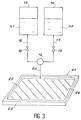
- the monomer 100, initiator 101, accelerator 103, compound single interlayer 104, the interlayer compound elastomeric 105 and polymer 106 are kept in two storage tanks 13 and 14 in storage conditions such as said monomer 100 is substantially stable over time, i.e. such that the polymerization of said monomer 100 has no not take place significantly.
- the number of tanks is not limited to two.
- Each tank 13 or 14 can contain a solution comprising one or more of the compounds following: monomer 100, initiator 101, accelerator 103, single interlayer compound 104, compound elastomeric interlayer 105, and polymer 106.
- a reservoir 13, 14 cannot contain at the same time time monomer 100, accelerator 103, and initiator 101.
- initiator 101 is preferably introduced into the solution least reactive monomer.
- the tanks advantageously comprise both the monomer 100 and polymer 106 so that the viscosity of the two solutions are close.
- the tank 13 includes a solution S1 comprising the compounds 100, 101, 104, 105 and 106, while the reservoir 14 contains a solution S2 comprising the compounds 100, 103, 104, 105 and 106.
- the tanks 13 and 14 are connected to a head of mixing 15 by respectively referenced conduits 16 and 17.
- the flow rate of mixture M1 in line 16 is regulated by a valve 18, while the flow of the mixture M2 in line 17 is regulated by a valve 19.
- the mixture of solutions S1 and S2, and therefore of the initiator 101 and accelerator 103, takes place in the head of mixing 15 according to an S1 / S2 ratio controlled by the valves 18 and 19.
- This mixture has a temperature Tmel.
- Tmél. is 25 ° C.
- the final mixture comprising both the initiator 101 and the accelerator 103 reacts quickly and the polymerized layer obtained can be thermosetting (crosslinked) and not soluble
- a mixing head is advantageously used 15 high pressure, self-cleaning.
- the polymerized layer obtained is thermoplastic (not crosslinked) and soluble, it is possible to use a low pressure mixing head.
- spreading is a simple dispensation of the mixture from the mixing head 15 and brought by a conduit 20 to a manufacturing support 21 for cards 1.
- This support 21 is then formed from an open cavity 22 of a half-mold 23, said crown, arranged on a sheet 24 intended to form a bottom layer of the card body 3.
- the spreading is carried out under reduced pressure, the order of atmospheric pressure.
- the manufacturing support 21 is formed by a honeycomb frame such as that described in the patent application French filed February 24, 1994 under number 94 02130 and in still other embodiments, the spreading is a pressure injection into a closed cavity of a card or layer that we want to obtain.
- micromodule 2 and, if necessary, antenna 12 may be present during spreading on the manufacturing support 21. They can however be inserted into the widespread mixture, while the polymerization of said mixture is not sufficient for bring its viscosity to too high values, greater than approximately 10,000 mPa.s.
- a lamination of the spilled mixture may be made, for example, between two rollers in order to quickly obtaining predetermined body thicknesses Map.
- a lamination is not conceives that with viscosities and speeds of particularly suitable polymerization and compatible, in particular, with spreading without flow, after said lamination, on a lower sheet, and with the covering of a set lower film - mixture laminated with a second film intended to form a top layer of the body of menu.
- a lamination can be carried out after a step of spreading in an open cavity a crown mold, and after applying a film upper intended to form a top layer of the card body, following demolding and cutting of bottom and top sheets. Note that in in this case, the applied films naturally adhere to the widespread mixtures, polymerization of said materials not being, at the stage of application of said sheets, totally finished.
- a radiation ignition can be done once the mixture has been spilled, for example, by opening an open cavity of the manufacturing support 21 of a card.
- the sets of valves 18, 19 allow, by varying their openings, to choose easily a compromise between all constraints cited in order to obtain a satisfactory product. From this point of view, the solution of the invention is well better than the old solutions listed. In effect, with these, with each new form or each new constraint, surface aspect to modify for example, it was necessary to redo many tedious testing, build many molds before to select an appropriate process and mold. Thanks the process adjustment possibilities according to the invention, good compromises are obtained quickly by simple steps to adjust the ratio.
- thermosets cure at temperatures below about 70 ° C and around 50 ° C approximately, while the viscosity of spilled materials is less than 10,000 mPa.s or even 5,000 mPa.s.
- MMA methacrylate methyl
- PMMA polymethyl methacrylate
- MMA polymerizes and PMMA is obtained.
- a simple radical initiator such as a peroxide, or ultraviolet radiation
- MMA polymerizes and PMMA is obtained.
- this polymerization is slow. For example, she is about 45 min. in the presence of peroxide benzoyl.
- the polymerization of MMA is accelerated by a tertiary amine such as, for example, N, N-bis (2-hydroxyethyl) -p-toluidine). Thanks to this amine, the polymerization time is considerably reduced. It is around 15 minutes. Nevertheless, the product obtained turns out to be brittle, we find a number significant bubbles, and a foul odor spreads.
- a tertiary amine such as, for example, N, N-bis (2-hydroxyethyl) -p-toluidine
- TEGMA triethylene glycol monomethyl methacrylate
- HEMA simple interlayer
- PBDM polybutadiene dimethacrylic
- TiO 2 titanium dioxide
- the solutions S1 and S2 stored at room temperature in the reservoirs 13 and 14 have the following composition, the percentages being given by weight: S1: MMA (100) 53.3% amine (103) 4.6% PMMA (106) 33.3% TiO 2 8.6% S2: MMA (100) 41.5% peroxide (101) 7.7% PBDM (105) 41.5% TiO 2 9.2%
- the polymerization of this mixture is carried out in less than 6 min. at a temperature below 50 ° C.
- MMA is liquid and its viscosity is less than about 100 mPa.s.
- the viscosity of this monomer is therefore much lower than the viscosities of thermoplastics used in the processes of prior art cards making which exceed 10,000 mPa.s.
- the gel effect is caused by triggering the very rapid polymerization of cyanoacrylate monomers (CNA) anionically, thanks with the intervention of a basic catalyst: an amine.
- CNA cyanoacrylate monomers
- a basic catalyst an amine.
- the PMMA / (CNA + MMA + PMMA) is not sufficient to trigger the effect of gel.
- the amine triggers a polymerization fast, even instantaneous, of the polycyanoacrylate DAC (PCNA).
- PCNA polycyanoacrylate DAC
- the ratio (PMMA + PCNA) / (MMA + PMMA + PCNA) becomes sufficient to generate a freezing effect in the mixture and accelerate the polymerization of MMA activated by the peroxide / amine combination.
- S1 solutions and S2, stored at room temperature in the tanks 13 and 14, have the following composition, the percentages given by weight:
- the polymerization of this mixture is then carried out in less than 5 min. at a temperature of the order of 55 ° C, the increase of 10 ° C compared to the the aforementioned temperature of 45 ° C. being due, in particular, to the CNA polymerization.
- HEMA is ultimately a compound elastomeric interlayer. Also, the polymerization of MMA will be total and no bad smell will come off.
- MMA was removed.
- the cards obtained by the process according to the invention using the acrylic system or methacrylic are, whether they are in contact or without, flexible, hard, impact resistant, and have a good surface condition.
- the monomers 100 are chosen for their characteristics and their impact on the layer polymerized 6. MMA is chosen for adhesion and rigidity, THFMA is chosen for membership, IBOMA is chosen for temperature resistance and TMPTMA, for rigidity. With a mixture of monomers 100, we thus finds a compromise for adhesion, rigidity and the temperature resistance of layer 6.
Landscapes
- Engineering & Computer Science (AREA)
- Computer Hardware Design (AREA)
- Microelectronics & Electronic Packaging (AREA)
- Physics & Mathematics (AREA)
- General Physics & Mathematics (AREA)
- Theoretical Computer Science (AREA)
- Polymerisation Methods In General (AREA)
- Credit Cards Or The Like (AREA)
Applications Claiming Priority (3)
| Application Number | Priority Date | Filing Date | Title |
|---|---|---|---|
| FR9501733 | 1995-02-15 | ||
| FR9501733A FR2730576B1 (fr) | 1995-02-15 | 1995-02-15 | Procede de fabrication de cartes electroniques et cartes obtenues par un tel procede |
| PCT/FR1996/000253 WO1996025721A1 (fr) | 1995-02-15 | 1996-02-15 | Procede de fabrication de cartes electroniques et cartes obtenues par un tel procede |
Publications (2)
| Publication Number | Publication Date |
|---|---|
| EP0809833A1 EP0809833A1 (fr) | 1997-12-03 |
| EP0809833B1 true EP0809833B1 (fr) | 1999-08-11 |
Family
ID=9476164
Family Applications (1)
| Application Number | Title | Priority Date | Filing Date |
|---|---|---|---|
| EP96904150A Expired - Lifetime EP0809833B1 (fr) | 1995-02-15 | 1996-02-15 | Procede de fabrication de cartes electroniques |
Country Status (8)
| Country | Link |
|---|---|
| US (1) | US6132799A (es) |
| EP (1) | EP0809833B1 (es) |
| JP (1) | JPH10503969A (es) |
| CA (1) | CA2212461A1 (es) |
| DE (1) | DE69603712T2 (es) |
| ES (1) | ES2138807T3 (es) |
| FR (1) | FR2730576B1 (es) |
| WO (1) | WO1996025721A1 (es) |
Families Citing this family (12)
| Publication number | Priority date | Publication date | Assignee | Title |
|---|---|---|---|---|
| FR2743336B1 (fr) * | 1996-01-04 | 1998-02-27 | Gemplus Card Int | Procede de fabrication d'une couche de revetement pour support portable, notamment support au format carte, et support portable muni d'une telle couche de revetement |
| FR2761497B1 (fr) * | 1997-03-27 | 1999-06-18 | Gemplus Card Int | Procede de fabrication d'une carte a puce ou analogue |
| DE19816417A1 (de) * | 1998-04-14 | 1999-10-28 | Angewandte Digital Elektronik | Chipkarte mit elektronischer Sperrfunktion |
| US6131811A (en) | 1998-05-29 | 2000-10-17 | E-Micro Corporation | Wallet consolidator |
| US6609654B1 (en) | 2000-05-15 | 2003-08-26 | Privasys, Inc. | Method for allowing a user to customize use of a payment card that generates a different payment card number for multiple transactions |
| US6755341B1 (en) | 2000-05-15 | 2004-06-29 | Jacob Y. Wong | Method for storing data in payment card transaction |
| US6805288B2 (en) | 2000-05-15 | 2004-10-19 | Larry Routhenstein | Method for generating customer secure card numbers subject to use restrictions by an electronic card |
| US6592044B1 (en) | 2000-05-15 | 2003-07-15 | Jacob Y. Wong | Anonymous electronic card for generating personal coupons useful in commercial and security transactions |
| FR2844621A1 (fr) * | 2002-09-13 | 2004-03-19 | A S K | Procede de fabrication d'une carte a puce sans contact ou hybride contact-sans contact a planeite renforcee |
| KR20040038134A (ko) * | 2002-10-31 | 2004-05-08 | 주식회사 쓰리비 시스템 | 안정된 비접촉 통신수단을 제공하는 콤비형 스마트 카드 |
| JP2006192320A (ja) * | 2005-01-11 | 2006-07-27 | Seiko Epson Corp | 識別コード描画方法、基板及び表示モジュール |
| FR2895547B1 (fr) * | 2005-12-26 | 2008-06-06 | Oberthur Card Syst Sa | Procede de fabrication d'une carte a microcircuit |
Citations (1)
| Publication number | Priority date | Publication date | Assignee | Title |
|---|---|---|---|---|
| EP0570784A1 (fr) * | 1992-05-19 | 1993-11-24 | François Droz | Carte comprenant au moins un élément électronique, et procédé de fabrication d'une telle carte |
Family Cites Families (7)
| Publication number | Priority date | Publication date | Assignee | Title |
|---|---|---|---|---|
| IE50670B1 (en) * | 1979-12-24 | 1986-06-11 | Agfa Gevaert Ag | Process for the production of forgery-proof documents |
| DE3336647A1 (de) * | 1983-10-08 | 1985-04-25 | Hoechst Ag, 6230 Frankfurt | Formmasse auf der basis von vinylchloridpolymerisaten und verfahren zur herstellung von folien aus diesen formmassen fuer die bereitung von faelschungssicheren wertpapieren |
| FR2624284B1 (fr) * | 1987-12-03 | 1991-08-16 | Sgs Thomson Microelectronics | Carte comportant un composant electronique |
| US5067008A (en) * | 1989-08-11 | 1991-11-19 | Hitachi Maxell, Ltd. | Ic package and ic card incorporating the same thereinto |
| FR2684235B1 (fr) * | 1991-11-25 | 1999-12-10 | Gemplus Card Int | Carte a circuit integre comprenant des moyens de protection du circuit integre. |
| US5317400A (en) * | 1992-05-22 | 1994-05-31 | Thomson Consumer Electronics, Inc. | Non-linear customer contrast control for a color television with autopix |
| US5534372A (en) * | 1993-07-28 | 1996-07-09 | Konica Corporation | IC card having image information |
-
1995
- 1995-02-15 FR FR9501733A patent/FR2730576B1/fr not_active Expired - Fee Related
-
1996
- 1996-02-15 ES ES96904150T patent/ES2138807T3/es not_active Expired - Lifetime
- 1996-02-15 WO PCT/FR1996/000253 patent/WO1996025721A1/fr active IP Right Grant
- 1996-02-15 DE DE69603712T patent/DE69603712T2/de not_active Expired - Fee Related
- 1996-02-15 CA CA002212461A patent/CA2212461A1/fr not_active Abandoned
- 1996-02-15 EP EP96904150A patent/EP0809833B1/fr not_active Expired - Lifetime
- 1996-02-15 JP JP8524722A patent/JPH10503969A/ja active Pending
-
1999
- 1999-10-26 US US09/426,912 patent/US6132799A/en not_active Expired - Fee Related
Patent Citations (1)
| Publication number | Priority date | Publication date | Assignee | Title |
|---|---|---|---|---|
| EP0570784A1 (fr) * | 1992-05-19 | 1993-11-24 | François Droz | Carte comprenant au moins un élément électronique, et procédé de fabrication d'une telle carte |
Also Published As
| Publication number | Publication date |
|---|---|
| US6132799A (en) | 2000-10-17 |
| EP0809833A1 (fr) | 1997-12-03 |
| ES2138807T3 (es) | 2000-01-16 |
| FR2730576A1 (fr) | 1996-08-14 |
| FR2730576B1 (fr) | 1997-04-04 |
| JPH10503969A (ja) | 1998-04-14 |
| CA2212461A1 (fr) | 1996-08-22 |
| DE69603712T2 (de) | 2000-01-13 |
| WO1996025721A1 (fr) | 1996-08-22 |
| DE69603712D1 (de) | 1999-09-16 |
Similar Documents
| Publication | Publication Date | Title |
|---|---|---|
| EP0809833B1 (fr) | Procede de fabrication de cartes electroniques | |
| EP0618548B1 (fr) | Procédé et dispositif de fabrication de cartes à mémoire | |
| EP1018092B1 (fr) | Procede de fabrication d'un module ou etiquette electronique, module ou etiquette obtenu et support comportant un tel module ou etiquette | |
| JP2003502169A (ja) | コンタクトレンズおよび他の眼科製品を製造するための保護被覆を備えたレンズ鋳型 | |
| EP0035309A1 (fr) | Procédé de fabrication par moulage de lentille de contact et lentilles obtenues | |
| EP0519564B1 (fr) | Procédé de fabrication d'une carte à micro-circuit et carte à micro-circuit | |
| FR2492807A1 (fr) | Article stratifie en verre et polycarbonate et procede pour la realisation de l'element en polycarbonate | |
| FR2617763A1 (fr) | Procede de fabrication de lentille de contact en un polymere proteique naturel, par moulage avant reticulation | |
| EP1242223B1 (en) | Method for molding materials on a planar substrate | |
| EP0917687B1 (fr) | Perfectionnement a un procede de realisation de cartes a memoire | |
| EP1186032B1 (fr) | Procede de fabrication de dispositif electronique portable a circuit integre protege par resine photosensible | |
| US20080053490A1 (en) | Method for hydrating a contact lens | |
| EP3105277B1 (fr) | Composition d'ensimage pour fibres de renfort et ses applications | |
| EP2762208B1 (fr) | Procédé de fabrication d'une planche de glisse, et planche de glisse obtenue par ce procédé | |
| EP0325875B1 (fr) | Matériau polymère à réseaux interpénétrés polysiloxane-polyacrylique, son procédé de fabrication, et articles moulés obtenus | |
| JP5082575B2 (ja) | 光半導体装置及びその製造方法 | |
| EP0917686B1 (fr) | Procede de realisation de cartes a memoire | |
| EP0976102B1 (fr) | Procede de fabrication d'une couche de revetement pour support portable, notamment support au format carte | |
| JP4171936B2 (ja) | 樹脂接合型光学素子の樹脂成形用金型及び製造方法 | |
| EP3894170B1 (fr) | Procédé de fabrication d'un moule de lithographie pour impression nanométrique | |
| KR20120032422A (ko) | 렌즈의 제조 방법 및 렌즈의 제조 장치 | |
| EP0245139A1 (fr) | Composite polyfluorure de vinylidène-polymère non compatible, procédé de fabrication du composite | |
| EP1273425A1 (fr) | Structure multicouche pour le conditionnement de produits alimentaires et procédé de fabrication de ladite structure | |
| KR20230152103A (ko) | 안과용 디바이스 제조용 금형 | |
| FR2795671A1 (fr) | Procede de fabrication de pieces optiques pour eclairage ou signalisation de vehicules automobiles |
Legal Events
| Date | Code | Title | Description |
|---|---|---|---|
| PUAI | Public reference made under article 153(3) epc to a published international application that has entered the european phase |
Free format text: ORIGINAL CODE: 0009012 |
|
| 17P | Request for examination filed |
Effective date: 19970804 |
|
| AK | Designated contracting states |
Kind code of ref document: A1 Designated state(s): CH DE ES FR GB IT LI |
|
| 17Q | First examination report despatched |
Effective date: 19971215 |
|
| GRAG | Despatch of communication of intention to grant |
Free format text: ORIGINAL CODE: EPIDOS AGRA |
|
| GRAG | Despatch of communication of intention to grant |
Free format text: ORIGINAL CODE: EPIDOS AGRA |
|
| GRAH | Despatch of communication of intention to grant a patent |
Free format text: ORIGINAL CODE: EPIDOS IGRA |
|
| GRAH | Despatch of communication of intention to grant a patent |
Free format text: ORIGINAL CODE: EPIDOS IGRA |
|
| GRAA | (expected) grant |
Free format text: ORIGINAL CODE: 0009210 |
|
| AK | Designated contracting states |
Kind code of ref document: B1 Designated state(s): CH DE ES FR GB IT LI |
|
| REG | Reference to a national code |
Ref country code: CH Ref legal event code: NV Representative=s name: BUGNION S.A. Ref country code: CH Ref legal event code: EP |
|
| REF | Corresponds to: |
Ref document number: 69603712 Country of ref document: DE Date of ref document: 19990916 |
|
| GBT | Gb: translation of ep patent filed (gb section 77(6)(a)/1977) |
Effective date: 19991020 |
|
| ITF | It: translation for a ep patent filed |
Owner name: PORTA CHECCACCI & ASSOCIATI S.P.A. |
|
| REG | Reference to a national code |
Ref country code: ES Ref legal event code: FG2A Ref document number: 2138807 Country of ref document: ES Kind code of ref document: T3 |
|
| PLBE | No opposition filed within time limit |
Free format text: ORIGINAL CODE: 0009261 |
|
| STAA | Information on the status of an ep patent application or granted ep patent |
Free format text: STATUS: NO OPPOSITION FILED WITHIN TIME LIMIT |
|
| 26N | No opposition filed | ||
| REG | Reference to a national code |
Ref country code: GB Ref legal event code: IF02 |
|
| PGFP | Annual fee paid to national office [announced via postgrant information from national office to epo] |
Ref country code: CH Payment date: 20040127 Year of fee payment: 9 |
|
| PGFP | Annual fee paid to national office [announced via postgrant information from national office to epo] |
Ref country code: GB Payment date: 20040128 Year of fee payment: 9 |
|
| PGFP | Annual fee paid to national office [announced via postgrant information from national office to epo] |
Ref country code: DE Payment date: 20040212 Year of fee payment: 9 |
|
| PGFP | Annual fee paid to national office [announced via postgrant information from national office to epo] |
Ref country code: ES Payment date: 20040218 Year of fee payment: 9 |
|
| PGFP | Annual fee paid to national office [announced via postgrant information from national office to epo] |
Ref country code: FR Payment date: 20040223 Year of fee payment: 9 |
|
| PG25 | Lapsed in a contracting state [announced via postgrant information from national office to epo] |
Ref country code: IT Free format text: LAPSE BECAUSE OF NON-PAYMENT OF DUE FEES;WARNING: LAPSES OF ITALIAN PATENTS WITH EFFECTIVE DATE BEFORE 2007 MAY HAVE OCCURRED AT ANY TIME BEFORE 2007. THE CORRECT EFFECTIVE DATE MAY BE DIFFERENT FROM THE ONE RECORDED. Effective date: 20050215 Ref country code: GB Free format text: LAPSE BECAUSE OF NON-PAYMENT OF DUE FEES Effective date: 20050215 |
|
| PG25 | Lapsed in a contracting state [announced via postgrant information from national office to epo] |
Ref country code: ES Free format text: LAPSE BECAUSE OF NON-PAYMENT OF DUE FEES Effective date: 20050216 |
|
| PG25 | Lapsed in a contracting state [announced via postgrant information from national office to epo] |
Ref country code: LI Free format text: LAPSE BECAUSE OF NON-PAYMENT OF DUE FEES Effective date: 20050228 Ref country code: CH Free format text: LAPSE BECAUSE OF NON-PAYMENT OF DUE FEES Effective date: 20050228 |
|
| PG25 | Lapsed in a contracting state [announced via postgrant information from national office to epo] |
Ref country code: DE Free format text: LAPSE BECAUSE OF NON-PAYMENT OF DUE FEES Effective date: 20050901 |
|
| GBPC | Gb: european patent ceased through non-payment of renewal fee |
Effective date: 20050215 |
|
| REG | Reference to a national code |
Ref country code: CH Ref legal event code: PL |
|
| PG25 | Lapsed in a contracting state [announced via postgrant information from national office to epo] |
Ref country code: FR Free format text: LAPSE BECAUSE OF NON-PAYMENT OF DUE FEES Effective date: 20051031 |
|
| REG | Reference to a national code |
Ref country code: FR Ref legal event code: ST Effective date: 20051031 |
|
| REG | Reference to a national code |
Ref country code: ES Ref legal event code: FD2A Effective date: 20050216 |