EP0809358A2 - Méthode de transmission d'un signal d'horloge et dispositif l'utilisant - Google Patents
Méthode de transmission d'un signal d'horloge et dispositif l'utilisant Download PDFInfo
- Publication number
- EP0809358A2 EP0809358A2 EP97107672A EP97107672A EP0809358A2 EP 0809358 A2 EP0809358 A2 EP 0809358A2 EP 97107672 A EP97107672 A EP 97107672A EP 97107672 A EP97107672 A EP 97107672A EP 0809358 A2 EP0809358 A2 EP 0809358A2
- Authority
- EP
- European Patent Office
- Prior art keywords
- pulse
- clock signal
- signal
- pieces
- signals
- Prior art date
- Legal status (The legal status is an assumption and is not a legal conclusion. Google has not performed a legal analysis and makes no representation as to the accuracy of the status listed.)
- Withdrawn
Links
Images

Classifications
-
- H—ELECTRICITY
- H04—ELECTRIC COMMUNICATION TECHNIQUE
- H04L—TRANSMISSION OF DIGITAL INFORMATION, e.g. TELEGRAPHIC COMMUNICATION
- H04L7/00—Arrangements for synchronising receiver with transmitter
-
- H—ELECTRICITY
- H04—ELECTRIC COMMUNICATION TECHNIQUE
- H04L—TRANSMISSION OF DIGITAL INFORMATION, e.g. TELEGRAPHIC COMMUNICATION
- H04L7/00—Arrangements for synchronising receiver with transmitter
- H04L7/0008—Synchronisation information channels, e.g. clock distribution lines
-
- H—ELECTRICITY
- H03—ELECTRONIC CIRCUITRY
- H03K—PULSE TECHNIQUE
- H03K5/00—Manipulating of pulses not covered by one of the other main groups of this subclass
- H03K5/00006—Changing the frequency
-
- H—ELECTRICITY
- H04—ELECTRIC COMMUNICATION TECHNIQUE
- H04L—TRANSMISSION OF DIGITAL INFORMATION, e.g. TELEGRAPHIC COMMUNICATION
- H04L7/00—Arrangements for synchronising receiver with transmitter
- H04L7/02—Speed or phase control by the received code signals, the signals containing no special synchronisation information
- H04L7/033—Speed or phase control by the received code signals, the signals containing no special synchronisation information using the transitions of the received signal to control the phase of the synchronising-signal-generating means, e.g. using a phase-locked loop
Definitions
- the present invention relates to a clock signal transmission technique, and more particularly to a high frequency clock signal transmission technique.
- the transmitting side sends two signals, namely, a clock signal and its inverted signal, to the receiving side via respective transmission lines.
- the two received signals are respectively frequency divided by 2
- the clock signal on the receiving side is obtained by subjecting these signals frequency divided by 2 to exclusive OR operation.
- the main object of the present invention is to provide a clock signal transmission method, and a device adopting the same, which can mitigate the effect of the waveform distortion on the transmission lines even when the frequency of the transmitted clock signal becomes high.
- a transmitting side clock signal of period T is frequency divided by 2n (n is a nonzero integer) to convert it to a first pulse signal of period 2nT, and n pieces of second pulse signals are generated by giving delays of 0, T, 2T, ...., and (n-1)T to the first pulse signal and these n pieces of second pulse signals are transmitted via a plurality of transmission lines.
- these n pieces of second pulse signals are received to detect the leading edges and trailing edges of these pulse signals, and the receiving side clock signal is generated based on timing signals that show the leading and trailing edges of these n pieces of second pulse signals.
- the waveform distortion is made less likely to occur on the transmission lines since the frequencies of the n pieces of the pulse signals transmitted via the transmission lines are 1/2n of the frequency of the transmitting side clock signal. Consequently, this invention is capable of generating the receiving side clock signal with more precise timings than in the prior art.
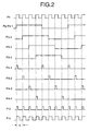
- FIG. 1 is a block diagram showing an embodiment of this invention.
- the equipment on the transmitting side includes a frequency divider 1 which divides the frequency of a transmitting side clock signal P1 by 2n and outputs a first pulse signal P2; and a shift register 2 which receives the first pulse signal P2, generates n second pulse signals P3-1, P3-2, ..., and P3-n by giving delays 0, T, 2T, ..., and (n-1)T to the first pulse signal P2, based on the clock signal P1 on the transmitting side, and outputs them to transmission lines 101, 102, ..., and 10n, respectively.
- the frequency divider 1 divides the frequency of the clock signal P1 with period T by 2n to generate a first pulse signal P2 of pulse width nT and duty ratio 50%, and outputs it to the shift register 2.
- the shift register 2 having n output terminals generates n second pulse signals P3-1, P3-2, ..., and P3-n by giving delays 0, T, 2T, ..., and (n-1)T to the first pulse signal P2, and outputs them from n output terminals to the transmission lines 101, 102, ..., and 10n.
- the frequency of the clock signal P1 with period T is divided by 2 x 4 by the frequency divider 1 to convert it to a first pulse signal P1 of pulse width 4T and duty ratio 50%.
- the shift register 2 sequentially shifts the first pulse signal P2 to generate n second pulse signals P3-1, P3-2, P3-3, and P3-4 by delaying the first pulse signal P1 by 0, T, 2T, and 3T, respectively, and outputs them to 4 transmission lines 101, 102, 103, and 104, respectively.
- the receiving side equipment includes n edge detectors 3-1, 3-2, ..., and 3-n which detect the leading edges and the trailing edges of the reception signals P3-1, P3-2, ..., and P3-n supplied by the transmission lines 101, 102, ..., and 10n, and output edge detection signals P4-1, P4-2, ..., and P4-n; a logic circuit 4 which generates a third pulse signal P5 by combining the edge detection signals P4-1, P4-2, ..., and P4-n; and a clock regenerator 6 which generates a regenerated clock signal P6 based on the third pulse signal P5.
- the clock regenerator 5 has a built-in phase locked loop (PLL), controls the oscillation frequency of a voltage controlled oscillator (VCO) within the PLL based on the third pulse signal P5, and generates a regenerated clock signal P6 which has the same frequency as that of the clock signal P1.
- PLL phase locked loop
- VCO voltage controlled oscillator
- the edge detectors 3-1, 3-2, 3-3, and 3-4 receive the second pulse signals P3-1, P3-2, P3-3, and P3-4, transmitted through the transmission lines 101, 102, 103, and 104, respectively, and output edge detection signals P4-1, P4-2, P4-3, and P4-4 by detecting respective leading edges and trailing edges of the second pulse signals.
- These edge detection signals are combined by an OR circuit 4 and the result is output as the third pulse signal P5.
- the frequency of this timing signal P5 agrees with the frequency of the transmitting side clock signal P1.
- This timing signal P5 is supplied to the clock regenerator 5 having the built-in PLL which generates the receiving side clock signal P6 of duty ratio 50%.
- a clock signal having a frequency 1/T is frequency-divided by 2n to generate a pulse signal of frequency 1/2nT and duty ratio of 50%.
- the pulse signal of frequency 1/2nT is delayed by 0, T, 2T, ..., and (n-1)T and the resulting signals are transmitted via n transmission lines. In this way, it is possible to transmit a clock signal by alleviating the influence of waveform distortion which is generated on the transmission lines.
Landscapes
- Engineering & Computer Science (AREA)
- Computer Networks & Wireless Communication (AREA)
- Signal Processing (AREA)
- Physics & Mathematics (AREA)
- Nonlinear Science (AREA)
- Synchronisation In Digital Transmission Systems (AREA)
- Manipulation Of Pulses (AREA)
Applications Claiming Priority (2)
| Application Number | Priority Date | Filing Date | Title |
|---|---|---|---|
| JP125777/96 | 1996-05-21 | ||
| JP12577796A JPH09312635A (ja) | 1996-05-21 | 1996-05-21 | クロック信号伝送装置 |
Publications (2)
| Publication Number | Publication Date |
|---|---|
| EP0809358A2 true EP0809358A2 (fr) | 1997-11-26 |
| EP0809358A3 EP0809358A3 (fr) | 1999-01-07 |
Family
ID=14918589
Family Applications (1)
| Application Number | Title | Priority Date | Filing Date |
|---|---|---|---|
| EP97107672A Withdrawn EP0809358A3 (fr) | 1996-05-21 | 1997-05-09 | Méthode de transmission d'un signal d'horloge et dispositif l'utilisant |
Country Status (6)
| Country | Link |
|---|---|
| US (1) | US5781049A (fr) |
| EP (1) | EP0809358A3 (fr) |
| JP (1) | JPH09312635A (fr) |
| KR (1) | KR100221821B1 (fr) |
| AU (1) | AU715717B2 (fr) |
| CA (1) | CA2203725C (fr) |
Cited By (1)
| Publication number | Priority date | Publication date | Assignee | Title |
|---|---|---|---|---|
| GB2397418A (en) * | 2003-01-15 | 2004-07-21 | Agilent Technologies Inc | Clock divider circuit |
Families Citing this family (10)
| Publication number | Priority date | Publication date | Assignee | Title |
|---|---|---|---|---|
| US5939919A (en) * | 1996-09-12 | 1999-08-17 | Hyundai Electronics America Inc | Clock signal distribution method for reducing active power dissipation |
| US6067648A (en) * | 1998-03-02 | 2000-05-23 | Tanisys Technology, Inc. | Programmable pulse generator |
| US6608514B1 (en) * | 1999-02-23 | 2003-08-19 | Kabushiki Kaisha Toshiba | Clock signal generator circuit and semiconductor integrated circuit with the same circuit |
| TWI245178B (en) * | 2004-01-16 | 2005-12-11 | Realtek Semiconductor Corp | Clock generation method and apparatus |
| US7299875B2 (en) * | 2004-06-08 | 2007-11-27 | Halliburton Energy Services, Inc. | Methods for controlling particulate migration |
| US8228561B2 (en) * | 2007-03-30 | 2012-07-24 | Xerox Corporation | Method and system for selective bitmap edge smoothing |
| US20090015066A1 (en) * | 2007-07-10 | 2009-01-15 | Yazaki North America, Inc. | Close-loop relay driver with equal-phase interval |
| JP2013037734A (ja) * | 2011-08-05 | 2013-02-21 | Elpida Memory Inc | 半導体装置 |
| US11989148B2 (en) | 2020-12-30 | 2024-05-21 | Stmicroelectronics International N.V. | Data bridge for interfacing source synchronous datapaths with unknown clock phases |
| US12210373B2 (en) | 2022-02-11 | 2025-01-28 | Stmicroelectronics International N.V. | Low overhead mesochronous digital interface |
Family Cites Families (5)
| Publication number | Priority date | Publication date | Assignee | Title |
|---|---|---|---|---|
| CA1129036A (fr) * | 1978-05-30 | 1982-08-03 | Colin R. Betts | Transmission de donnees numeriques |
| JPS6170816A (ja) * | 1984-09-13 | 1986-04-11 | Futaba Corp | 符号再生装置 |
| JPH0410011A (ja) * | 1990-04-27 | 1992-01-14 | Oki Electric Ind Co Ltd | クロック信号分配回路 |
| DE4041625A1 (de) * | 1990-12-22 | 1992-07-02 | Ant Nachrichtentech | Asynchrone uebertragung ueber ein synchrones digitalsignal-uebertragungssystem |
| JPH0831847B2 (ja) * | 1991-10-09 | 1996-03-27 | 株式会社ネットワークサプライ | ディジタル信号中継伝送装置 |
-
1996
- 1996-05-21 JP JP12577796A patent/JPH09312635A/ja active Pending
-
1997
- 1997-04-25 CA CA002203725A patent/CA2203725C/fr not_active Expired - Fee Related
- 1997-04-25 US US08/844,697 patent/US5781049A/en not_active Expired - Fee Related
- 1997-05-09 EP EP97107672A patent/EP0809358A3/fr not_active Withdrawn
- 1997-05-19 KR KR1019970019342A patent/KR100221821B1/ko not_active Expired - Fee Related
- 1997-05-20 AU AU23525/97A patent/AU715717B2/en not_active Ceased
Cited By (2)
| Publication number | Priority date | Publication date | Assignee | Title |
|---|---|---|---|---|
| GB2397418A (en) * | 2003-01-15 | 2004-07-21 | Agilent Technologies Inc | Clock divider circuit |
| GB2397418B (en) * | 2003-01-15 | 2006-09-27 | Agilent Technologies Inc | Clock circuit |
Also Published As
| Publication number | Publication date |
|---|---|
| KR100221821B1 (ko) | 1999-09-15 |
| JPH09312635A (ja) | 1997-12-02 |
| AU715717B2 (en) | 2000-02-10 |
| AU2352597A (en) | 1997-11-27 |
| KR970078197A (ko) | 1997-12-12 |
| CA2203725C (fr) | 2001-07-03 |
| CA2203725A1 (fr) | 1997-11-21 |
| US5781049A (en) | 1998-07-14 |
| EP0809358A3 (fr) | 1999-01-07 |
Similar Documents
| Publication | Publication Date | Title |
|---|---|---|
| KR102599904B1 (ko) | 다상 클록 듀티 사이클 및 스큐 측정 및 보정 | |
| EP0709966B1 (fr) | Détecteur de phase à sortie ternaire | |
| EP0679307B1 (fr) | Separateur de lignes de retard pour bus de donnees | |
| US6463092B1 (en) | System and method for sending and receiving data signals over a clock signal line | |
| US5781049A (en) | Method of transmitting clock signal and device employing the same | |
| US7143312B1 (en) | Alignment of recovered clock with data signal | |
| US7482841B1 (en) | Differential bang-bang phase detector (BBPD) with latency reduction | |
| US5808571A (en) | Synchronization control unit which maintains synchronization between serial-to-parallel converters operating in parallel, or between parallel-to-serial converters operating in parallel | |
| EP1051004A2 (fr) | Recepteur et procédé de réception d'un signal FSK | |
| KR100400043B1 (ko) | 데이터 복원 회로 및 방법 | |
| US5640523A (en) | Method and apparatus for a pulsed tri-state phase detector for reduced jitter clock recovery | |
| US7280589B2 (en) | Source synchronous I/O bus retimer | |
| US7861105B2 (en) | Clock data recovery (CDR) system using interpolator and timing loop module | |
| JPH06505381A (ja) | 位相独立性帯域制御を有するデータ伝送システム受信機 | |
| US7139308B2 (en) | Source synchronous bus repeater | |
| US6137332A (en) | Clock signal generator and data signal generator | |
| US6266383B1 (en) | Clock reproduction circuit and data transmission apparatus | |
| US20070127612A1 (en) | Apparatus and method for retiming data using phase-interpolated clock signal | |
| US20070230646A1 (en) | Phase recovery from forward clock | |
| KR100243001B1 (ko) | 복수 채널용 심볼 타이밍 복구회로 | |
| US7359461B2 (en) | Apparatus and method for recovering clock signal from burst mode signal | |
| US4818894A (en) | Method and apparatus for obtaining high frequency resolution of a low frequency signal | |
| US7116738B1 (en) | Data synchronization apparatus and method | |
| JP5515920B2 (ja) | Dpll回路 | |
| KR910006000B1 (ko) | 고속 데이타-클럭동기프로세서 |
Legal Events
| Date | Code | Title | Description |
|---|---|---|---|
| PUAI | Public reference made under article 153(3) epc to a published international application that has entered the european phase |
Free format text: ORIGINAL CODE: 0009012 |
|
| AK | Designated contracting states |
Kind code of ref document: A2 Designated state(s): DE FR GB IT NL SE |
|
| PUAL | Search report despatched |
Free format text: ORIGINAL CODE: 0009013 |
|
| AK | Designated contracting states |
Kind code of ref document: A3 Designated state(s): DE FR GB IT NL SE |
|
| RHK1 | Main classification (correction) |
Ipc: H04L 25/02 |
|
| 17P | Request for examination filed |
Effective date: 19990422 |
|
| STAA | Information on the status of an ep patent application or granted ep patent |
Free format text: STATUS: THE APPLICATION HAS BEEN WITHDRAWN |
|
| 18W | Application withdrawn |
Withdrawal date: 20011126 |