EP0809315A1 - Dielektrischer Filter - Google Patents
Dielektrischer Filter Download PDFInfo
- Publication number
- EP0809315A1 EP0809315A1 EP97303506A EP97303506A EP0809315A1 EP 0809315 A1 EP0809315 A1 EP 0809315A1 EP 97303506 A EP97303506 A EP 97303506A EP 97303506 A EP97303506 A EP 97303506A EP 0809315 A1 EP0809315 A1 EP 0809315A1
- Authority
- EP
- European Patent Office
- Prior art keywords
- resonators
- coupling
- outermost
- ceramic block
- open
- Prior art date
- Legal status (The legal status is an assumption and is not a legal conclusion. Google has not performed a legal analysis and makes no representation as to the accuracy of the status listed.)
- Granted
Links
- 230000008878 coupling Effects 0.000 claims abstract description 93
- 238000010168 coupling process Methods 0.000 claims abstract description 93
- 238000005859 coupling reaction Methods 0.000 claims abstract description 93
- 239000000919 ceramic Substances 0.000 claims abstract description 44
- 239000004020 conductor Substances 0.000 claims description 63
- 230000002093 peripheral effect Effects 0.000 claims description 9
- 239000011248 coating agent Substances 0.000 description 3
- 238000000576 coating method Methods 0.000 description 3
- 230000005540 biological transmission Effects 0.000 description 2
- 238000010586 diagram Methods 0.000 description 2
- 239000003989 dielectric material Substances 0.000 description 2
- GWEVSGVZZGPLCZ-UHFFFAOYSA-N Titan oxide Chemical compound O=[Ti]=O GWEVSGVZZGPLCZ-UHFFFAOYSA-N 0.000 description 1
- 230000015556 catabolic process Effects 0.000 description 1
- 238000006731 degradation reaction Methods 0.000 description 1
- 230000000694 effects Effects 0.000 description 1
- 239000000463 material Substances 0.000 description 1
- OGIDPMRJRNCKJF-UHFFFAOYSA-N titanium oxide Inorganic materials [Ti]=O OGIDPMRJRNCKJF-UHFFFAOYSA-N 0.000 description 1
Images


Classifications
-
- H—ELECTRICITY
- H01—ELECTRIC ELEMENTS
- H01P—WAVEGUIDES; RESONATORS, LINES, OR OTHER DEVICES OF THE WAVEGUIDE TYPE
- H01P1/00—Auxiliary devices
- H01P1/20—Frequency-selective devices, e.g. filters
- H01P1/213—Frequency-selective devices, e.g. filters combining or separating two or more different frequencies
- H01P1/2136—Frequency-selective devices, e.g. filters combining or separating two or more different frequencies using comb or interdigital filters; using cascaded coaxial cavities
-
- H—ELECTRICITY
- H01—ELECTRIC ELEMENTS
- H01P—WAVEGUIDES; RESONATORS, LINES, OR OTHER DEVICES OF THE WAVEGUIDE TYPE
- H01P1/00—Auxiliary devices
- H01P1/20—Frequency-selective devices, e.g. filters
- H01P1/201—Filters for transverse electromagnetic waves
- H01P1/205—Comb or interdigital filters; Cascaded coaxial cavities
- H01P1/2056—Comb filters or interdigital filters with metallised resonator holes in a dielectric block
Definitions
- the present invention relates to a dielectric filter comprising a plurality of juxtaposed resonators, and a duplexer using such resonators.
- FIG. 1 of the accompanying drawings illustrates a known typical dielectric filter comprising a dielectric ceramic block A, three or more than three resonators B provided in the block A respectively by coating the peripheral walls of three or more than three through bores with a conducting material, an external conductor C covering the outer surfaces of the dielectric ceramic block A but not open-circuit end surface having the openings of the through bores, a pair of coupling through bores D arranged between adjacent ones of the resonators B in parallel with the latter and having no coating on the peripheral walls thereof and a pair of input/output pads E arranged on a lateral surface of the dielectric ceramic block A at respective positions abutting the open-circuit end surface of the block A and facing the respective outermost resonators in such a way that they are electrically insulated from the external conductor C.
- the magnetic field coupling intensity of the adjacent resonators may be intensified because dielectrics are cleared off between adjacent resonators B by a coupling through bore D.
- a dielectric filter comprising a dielectric ceramic block, three or more than three resonators provided in said dielectric ceramic block respectively, each resonator including a through bore and an inner conductor on a peripheral wall of the through bore, an external conductor covering the outer surfaces of said dielectric ceramic block excepting an open-circuit end surface having openings of the through bores, coupling through bores arranged between adjacent ones of said resonators in parallel with the latter and a pair of input/output pads arranged on a lateral surface of said dielectric ceramic block at respective positions abutting the open-circuit end surface of the block and facing the respective outermost resonators in such a way that they are electrically insulated from said external conductor, wherein the filter comprises outer coupling electric paths extending from said respective input/output pads onto the open-circuit end surface and arranged in juxtaposition with the respective outermost resonators with a coupling gap provided therebetween and inner coupling electric paths extending from the respective input/
- the dielectric filter further may comprise a rectangularly extended conductor arranged on the open-circuit end surface of said dielectric ceramic block to surround the internal conductor of said inner resonator or each of said respective inner resonators and connected to the internal conductor of said inner resonator or each of said respective inner resonators.
- each of said inner coupling electric paths may be arranged to be adjacent to said respective rectangularly extended conductor on the open-circuit end surface of said dielectric ceramic block.
- each of said outer coupling electric paths may be provided with an arcuate coupling tip to surround the opening of the associated through bore with the coupling gap therebetween.
- Futhermore, rectangularly extended conductors may be arranged on the open-circuit end surface of said dielectric ceramic block to surround the internal conductors of said respective outermost resonators and connected to the internal conductors of said respective outermost resonators.
- the input/output pads may be disposed on an outer surface portion of the dielectric ceramic block to be brought into contact with a printed circuit board when the filter is mounted on the circuit board.
- the input/output pads may be disposed on other outer surface portion than that to be brought into contact with a printed circuit board when the filter is mounted on the circuit board.
- Each of said rectangularly extended conductors arranged to surround the internal conductors of said respective outermost resonators and connected thereto may be provided with at least one notch, and each of said outer coupling electric paths may be provided with a corresponding coupling projection which is engaged with said notch.
- a dielectric filter for a duplexer having a transmitter section and a receiver section provided on a dielectric ceramic block, said transmitter section having three or more than three resonators juxtaposed to each other in the dielectric ceramic block, each of which includes a through bore and an inner conductor provided on inner peripheral wall of the through bore, said dielectric ceramic block being provided with an external conductor covering an outer surface excepting an open-circuit end surface thereof, coupling through bores arranged between adjacent ones of the resonators in parallel with the latter and a pair of input/output pads arranged on a lateral surface of said dielectric ceramic block at respective positions abutting the open-circuit end surface of the block and facing the respective outermost and innermost resonators in such a way that they are electrically insulated from the external conductor, wherein said transmitter section comprises outer coupling electric paths extending from said respective input/output pads onto the open-circuit end surface and arranged in juxtaposition with the respective outermost and innermost re
- the receiver section comprises a plurality of resonators provided in a row, one of the input/output pads is associated with the innermost resonators of the transmitter and receiver sections and is arranged to be operated as an input pad for said receiver section, and an output pad is capacitively coupled to the outermost resonator of the receiver section.
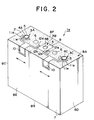
- FIGS. 2 and 3 shows a first embodiment of dielectric filter la according to the invention, which is a three pole type dielectric filter having three resonators.
- the illustrated dielectric filter la comprises a substantially rectangularly parallelepipedic dielectric ceramic block 2 made of a titanium oxide type material and provided with three resonators 3A, 3B and 3C that are arranged in parallel with each other.
- the resonators 3A, 3B and 3C are realized by forming through bores 4A, 4B and 4C running through the dielectric ceramic block 2 and coating the peripheral inner walls of the through bores 4A, 4B and 4C with a conductive material to produce internal conductors 5.
- a pair of coupling through bores 6 are arranged respectively between the resonators 3A and 3B and between the resonators 3B and 3C and in parallel with the through bores 4A, 4B and 4C to couple the adjacent resonators.
- No internal conductor is arranged on the coupling through bores 6 and 6. The coupling intensity of the adjacently located resonators 3A and 3B and that of the resonators 3B and 3C are boosted by the respective coupling through bores 6 and 6.
- An external conductor 7 is formed by covering the outer surfaces 8B-8F of the dielectric ceramic block 2 also with a conductive material but not an open-circuit end surface 8A having the openings of the through bores 4A, 4B and 4C.
- the external conductor 7 operates as a shield or ground electrode.
- the resonators 3A, 3B and 3C have a resonance length substantially equal to a quarter of the resonance frequency ⁇ or ⁇ /4.
- a rectangularly extended conductor 9 is arranged on the open-circuit end surface 8A of dielectric ceramic block 2, surrounding the open end of the resonator 3B, and connected to the internal conductor 5 thereof on the peripheral wall of the through bore 4B.
- a pair of input/output pads 10 are arranged on a lateral surface 8E (which is to be directly mounted on a printed circuit board not shown) of the dielectric ceramic block 2 vis-a-vis the respective outermost resonators 3A and 3C for capacitive coupling and insulated from the external conductor 7. Therefore, the input/output pads 10 are to be electrically connected to conductors arranged, for example, on the printed circuit board.
- outer coupling electric paths 11a which are respectively extending from the input/output pads 10 onto the open-circuit end surface 8A and arranged in juxtaposition with the respective openings of the outermost resonators 3A and 3C with a coupling gap provided therebetween.
- inner coupling electric paths 12a which are respectively extending from the respective input/output pads 10 onto the open-circuit end surface 8A and arranged between the outermost resonators 3A and 3C in the areas adjacent to the conductor 9 on the inner resonator 3B with a coupling gap provided therebetween.
- the free ends of the outer coupling electric paths 11a are provided with respective arcuate coupling tips 11e to surround the respective openings of the through bores 4A and 4C with a coupling gap gl disposed therebetween.
- the inner coupling electric paths 12a are L-shaped and provided with respective straight coupling tips 12e separated from the conductor 9 by a coupling gap g2.
- the input/output pads 10 are capacitively coupled to the respective resonators 3A and 3C by way of the respective outer coupling electric paths 11a and also to the resonator 3B by way of the respective inner coupling electric paths 12a.
- FIG. 4A shows the attenuation waveform of the illustrated dielectric filter.
- FIG. 4B shows the attenuation waveform of a comparable dielectric filter realized with no inner coupling electric paths.
- the waveform of FIG. 4B has a fly back x produced in a higher frequency zone of the resonance frequency band under the influence of the coupling through bores 6 to hold the output level above the threshold value of -50dB.
- the fly back x is reduced to less than -50dB in this illustrated embodiment to make the filter perform remarkably in terms of attenuation.
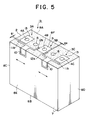
- FIG. 5 illustrates a second embodiment of dielectric filter 1b according to the invention having outer coupling electric paths 11b having a profile different from that of their counterparts of the first embodiment illustrated in FIGS. 2 and 3.
- rectangularly extended conductors 13 are arranged on the open-circuit end surface 8A of dielectric ceramic block 2, surrounding the respective open ends of the resonators 3A and 3C, and connected to the internal conductors 5 thereof on the peripheral walls of the through bores 4A and 4C.
- the outer coupling electric paths 11b are linearly formed and arranged in juxtaposition with the respective front edges of the rectangular conductors 13 with a coupling gap g1 provided therebetween.
- inner coupling electric paths 12b similar to their counterparts of the first embodiment are extending from the respective input/output pads 10 and arranged in juxtaposition with the respective lateral edges of the rectangular conductor 9 of the resonator 3B with a coupling gap g2 provided therebetween.
- the input/output pads 10 are capacitively coupled to the respective resonators 3A and 3C by way of the respective outer coupling electric paths 11a and 11b and also to the resonator 3B by way of the respective inner coupling electric paths 12a and 12b.
- the input/output pads 10 of each of the above embodiments can be displaced appropriately in the direction of the arrows in FIGS.
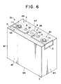
- FIG. 6 illustrates a third embodiment of dielectric filter 1c according to the invention, where the input/output pads 10 are arranged respectively on oppositely disposed lateral surfaces 8C and 8D of the dielectric ceramic block 2.
- the input/output pads 10 may be exposed on the printed circuit board on which the dielectric filter is arranged so that the related leads may be arranged easily to connect the dielectric filter and the printed circuit board by way of the input/output pads 10.
- outer coupling electric paths 11c and inner coupling electric paths 12c are extending respectively from the input/output pads 10 and juxtaposed with the respective resonators 3A, 3B and 3C with coupling gaps g1 and g2 provided therebetween for capacitive coupling in a manner as described above by referring to the first and second embodiments.
- FIG. 7 shows a circuit diagram of an equivalent circuit of the illustrated filter 1a.
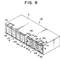
- FIGS. 8 and 9 schematically illustrate a fourth embodiment of dielectric filter 1d according to the invention which is to be used as a duplexer comprising a transmitter section T and a receiver section R.
- the transmitter section T include a pair of input/output pads 10a and 10b, outer and inner coupling electric paths 11d and 12d extending respectively from the input/output pads 10a and 10b and arranged respectively in juxtaposition with the substantially rectangular conductors 9 and 14 of resonators 3A, 3B and 3C for capacitive coupling in a manner as described earlier.
- the rectangular conductors 14 of the outermost resonators 3A and 3C may be provided with notches 15 and the outer coupling electric paths 11d may be provided with corresponding coupling projections 16 projecting into the respective notches 15, whereas the inner coupling electric paths 12d have a L-shaped profile as in the case of the preceding embodiments.
- the outer input/output pad 10a actually operates as an input pad whereas the inner input/output pad 10b operates as an output pad.
- the receiver section R of this embodiment has a four-poled structure in which four resonators 17A, 17B, 17C and 17D are provided in a row.
- An output pad 10c is capacitively coupled to the outermost resonator 17D of the receiver section R whereas the inner input/ output pad 10b of the transmitter section T is shared by the receiver section R and operating as an input pad of the latter.
- the rectangular conductors 14 of the outermost resonators 3A and 3C may be formed without any notches as in the arrangement of the second embodiment illustrated in FIG. 5.
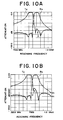
- FIG. 10A shows the waveform of the transmission wave Tx and that of the reception wave Rx of dielectric filter 1d in the fourth embodiment.
- FIG. 10B a comparable graph obtained by a dielectric filter realized by removing only the inner coupling electric paths 12d and 12d from the fourth embodiment.
- the resonators 3A, 3B and 3C are realized by using through bores having a circular cross section, the through bores may be replaced by through holes having a square, oval or rectangular cross section.
- the through bores may be replaced by through holes having a square, oval or rectangular cross section.
- the input/output pads and the inner resonator or resonators are capacitively coupled with the respective input/output pads to remarkably reduce or eliminate the influence of the fly back x or y and consequently improve the attenuation performance of the dielectric filter and reduce the generation of noise.
Landscapes
- Physics & Mathematics (AREA)
- Electromagnetism (AREA)
- Control Of Motors That Do Not Use Commutators (AREA)
Applications Claiming Priority (3)
| Application Number | Priority Date | Filing Date | Title |
|---|---|---|---|
| JP8153476A JPH09312506A (ja) | 1996-05-23 | 1996-05-23 | 誘電体フィルタ |
| JP15347696 | 1996-05-23 | ||
| JP153476/96 | 1996-05-23 |
Publications (2)
| Publication Number | Publication Date |
|---|---|
| EP0809315A1 true EP0809315A1 (de) | 1997-11-26 |
| EP0809315B1 EP0809315B1 (de) | 2002-04-17 |
Family
ID=15563415
Family Applications (1)
| Application Number | Title | Priority Date | Filing Date |
|---|---|---|---|
| EP97303506A Expired - Lifetime EP0809315B1 (de) | 1996-05-23 | 1997-05-22 | Dielektrisches Filter |
Country Status (4)
| Country | Link |
|---|---|
| US (1) | US5864264A (de) |
| EP (1) | EP0809315B1 (de) |
| JP (1) | JPH09312506A (de) |
| DE (1) | DE69711979T2 (de) |
Cited By (9)
| Publication number | Priority date | Publication date | Assignee | Title |
|---|---|---|---|---|
| WO1999048166A1 (de) * | 1998-03-18 | 1999-09-23 | Epcos Ag | Mikrowellen-keramikfilter mit verbesserter flankensteilheit |
| GB2339341A (en) * | 1998-07-08 | 2000-01-19 | Samsung Electro Mech | Duplexer dielectric filter |
| US6169465B1 (en) | 1998-07-08 | 2001-01-02 | Samsung Electro-Mechanics Co., Ltd. | Duplexer dielectric filter |
| EP0982792A3 (de) * | 1998-08-25 | 2001-08-01 | Murata Manufacturing Co., Ltd. | Antennenweiche und Kommunikationsgerät |
| GB2374985A (en) * | 2000-12-19 | 2002-10-30 | Murata Manufacturing Co | Dielectric filter, dielectric duplexer, and communication apparatus |
| US6501347B1 (en) | 1999-09-24 | 2002-12-31 | Ngk Spark Plug Co., Ltd. | Dielectric filter having forked auxiliary conductor |
| GB2382234A (en) * | 2001-03-15 | 2003-05-21 | Murata Manufacturing Co | Dielectric filter, dielectric duplexer, and communication apparatus using the same |
| AT411000B (de) * | 1998-07-08 | 2003-09-25 | Samsung Electro Mech | Dielektrisches filter |
| DE10313336A1 (de) * | 2003-03-25 | 2004-11-18 | Epcos Ag | Mikrowellenkeramik-Filter mit verbesserter Ankopplung und Verfahren zur Herstellung |
Families Citing this family (8)
| Publication number | Priority date | Publication date | Assignee | Title |
|---|---|---|---|---|
| JP3468143B2 (ja) * | 1999-01-28 | 2003-11-17 | 株式会社村田製作所 | 誘電体フィルタ、誘電体ディプレクサおよび通信機 |
| US6724279B1 (en) * | 2000-10-03 | 2004-04-20 | Ube Electronics, Ltd. | Duplexer filter with offset resonator holes |
| US6559735B1 (en) * | 2000-10-31 | 2003-05-06 | Cts Corporation | Duplexer filter with an alternative signal path |
| JP2003087010A (ja) * | 2001-09-06 | 2003-03-20 | Ngk Spark Plug Co Ltd | 誘電体デュプレクサ |
| US6650202B2 (en) * | 2001-11-03 | 2003-11-18 | Cts Corporation | Ceramic RF filter having improved third harmonic response |
| US20040183626A1 (en) * | 2003-02-05 | 2004-09-23 | Qinghua Kang | Electronically tunable block filter with tunable transmission zeros |
| US7545240B2 (en) | 2005-05-24 | 2009-06-09 | Cts Corporation | Filter with multiple shunt zeros |
| US7714680B2 (en) * | 2006-05-31 | 2010-05-11 | Cts Corporation | Ceramic monoblock filter with inductive direct-coupling and quadruplet cross-coupling |
Citations (5)
| Publication number | Priority date | Publication date | Assignee | Title |
|---|---|---|---|---|
| EP0367061A2 (de) * | 1988-10-31 | 1990-05-09 | Motorola, Inc. | Keramisches Filter mit integrierter Phasenverschiebungsschaltung |
| EP0442418A2 (de) * | 1990-02-14 | 1991-08-21 | Oki Electric Industry Company, Limited | Dielektrischer Filter mit Mustern zur Einstellung der Kopplung |
| JPH0495401A (ja) * | 1990-08-10 | 1992-03-27 | Murata Mfg Co Ltd | 有極型誘電体フィルタ |
| EP0552761A1 (de) * | 1992-01-23 | 1993-07-28 | Murata Manufacturing Co., Ltd. | Dielektrischer Resonator und Herstellungsverfahren dafür |
| US5250916A (en) * | 1992-04-30 | 1993-10-05 | Motorola, Inc. | Multi-passband dielectric filter construction having filter portions with dissimilarly-sized resonators |
Family Cites Families (11)
| Publication number | Priority date | Publication date | Assignee | Title |
|---|---|---|---|---|
| JPS60114004A (ja) * | 1983-11-25 | 1985-06-20 | Murata Mfg Co Ltd | 誘電体フィルタの実装構造 |
| JPS61208902A (ja) * | 1985-03-13 | 1986-09-17 | Murata Mfg Co Ltd | Mic型誘電体フイルタ |
| US4716391A (en) * | 1986-07-25 | 1987-12-29 | Motorola, Inc. | Multiple resonator component-mountable filter |
| JPS63306701A (ja) * | 1987-06-08 | 1988-12-14 | Fuji Elelctrochem Co Ltd | 誘電体フィルタ |
| US4879533A (en) * | 1988-04-01 | 1989-11-07 | Motorola, Inc. | Surface mount filter with integral transmission line connection |
| JPH02130103U (de) * | 1988-11-16 | 1990-10-26 | ||
| US5045824A (en) * | 1990-09-04 | 1991-09-03 | Motorola, Inc. | Dielectric filter construction |
| JPH0522002A (ja) * | 1991-07-15 | 1993-01-29 | Fuji Elelctrochem Co Ltd | 誘電体フイルタ |
| US5177458A (en) * | 1991-07-31 | 1993-01-05 | Motorola, Inc. | Dielectric filter construction having notched mounting surface |
| DE4229165C2 (de) * | 1992-09-01 | 1995-11-02 | Siemens Matsushita Components | Keramik-Koaxialresonator |
| US5499004A (en) * | 1993-03-12 | 1996-03-12 | Matsushita Electric Industrial Co., Ltd. | Dielectric filter having interstage coupling using adjacent electrodes |
-
1996
- 1996-05-23 JP JP8153476A patent/JPH09312506A/ja active Pending
-
1997
- 1997-05-22 US US08/862,150 patent/US5864264A/en not_active Expired - Fee Related
- 1997-05-22 EP EP97303506A patent/EP0809315B1/de not_active Expired - Lifetime
- 1997-05-22 DE DE69711979T patent/DE69711979T2/de not_active Expired - Fee Related
Patent Citations (5)
| Publication number | Priority date | Publication date | Assignee | Title |
|---|---|---|---|---|
| EP0367061A2 (de) * | 1988-10-31 | 1990-05-09 | Motorola, Inc. | Keramisches Filter mit integrierter Phasenverschiebungsschaltung |
| EP0442418A2 (de) * | 1990-02-14 | 1991-08-21 | Oki Electric Industry Company, Limited | Dielektrischer Filter mit Mustern zur Einstellung der Kopplung |
| JPH0495401A (ja) * | 1990-08-10 | 1992-03-27 | Murata Mfg Co Ltd | 有極型誘電体フィルタ |
| EP0552761A1 (de) * | 1992-01-23 | 1993-07-28 | Murata Manufacturing Co., Ltd. | Dielektrischer Resonator und Herstellungsverfahren dafür |
| US5250916A (en) * | 1992-04-30 | 1993-10-05 | Motorola, Inc. | Multi-passband dielectric filter construction having filter portions with dissimilarly-sized resonators |
Non-Patent Citations (1)
| Title |
|---|
| PATENT ABSTRACTS OF JAPAN vol. 16, no. 324 (E - 1234) 15 July 1992 (1992-07-15) * |
Cited By (15)
| Publication number | Priority date | Publication date | Assignee | Title |
|---|---|---|---|---|
| US6552633B1 (en) | 1998-03-18 | 2003-04-22 | Epcos Ag | Ceramic microwave filter having greater edge steepness |
| WO1999048166A1 (de) * | 1998-03-18 | 1999-09-23 | Epcos Ag | Mikrowellen-keramikfilter mit verbesserter flankensteilheit |
| GB2339341A (en) * | 1998-07-08 | 2000-01-19 | Samsung Electro Mech | Duplexer dielectric filter |
| US6169465B1 (en) | 1998-07-08 | 2001-01-02 | Samsung Electro-Mechanics Co., Ltd. | Duplexer dielectric filter |
| AT411000B (de) * | 1998-07-08 | 2003-09-25 | Samsung Electro Mech | Dielektrisches filter |
| AT411119B (de) * | 1998-07-08 | 2003-09-25 | Samsung Electro Mech | Dielektrisches duplexsystem-filter |
| GB2339341B (en) * | 1998-07-08 | 2003-07-09 | Samsung Electro Mech | A duplexer dielectric filter |
| EP0982792A3 (de) * | 1998-08-25 | 2001-08-01 | Murata Manufacturing Co., Ltd. | Antennenweiche und Kommunikationsgerät |
| US6501347B1 (en) | 1999-09-24 | 2002-12-31 | Ngk Spark Plug Co., Ltd. | Dielectric filter having forked auxiliary conductor |
| GB2374985B (en) * | 2000-12-19 | 2003-03-19 | Murata Manufacturing Co | Dielectric filter, dielectric duplexer, and communication apparatus |
| GB2374985A (en) * | 2000-12-19 | 2002-10-30 | Murata Manufacturing Co | Dielectric filter, dielectric duplexer, and communication apparatus |
| US6686813B2 (en) | 2000-12-19 | 2004-02-03 | Murata Manufacturing Co. Ltd. | Dielectric filter, dielectric duplexer, and communication apparatus |
| GB2382234A (en) * | 2001-03-15 | 2003-05-21 | Murata Manufacturing Co | Dielectric filter, dielectric duplexer, and communication apparatus using the same |
| GB2382234B (en) * | 2001-03-15 | 2003-12-31 | Murata Manufacturing Co | Dielectric filter, dielectric duplexer, and communication apparatus using the same |
| DE10313336A1 (de) * | 2003-03-25 | 2004-11-18 | Epcos Ag | Mikrowellenkeramik-Filter mit verbesserter Ankopplung und Verfahren zur Herstellung |
Also Published As
| Publication number | Publication date |
|---|---|
| JPH09312506A (ja) | 1997-12-02 |
| DE69711979D1 (de) | 2002-05-23 |
| EP0809315B1 (de) | 2002-04-17 |
| US5864264A (en) | 1999-01-26 |
| DE69711979T2 (de) | 2002-10-10 |
Similar Documents
| Publication | Publication Date | Title |
|---|---|---|
| EP0809315B1 (de) | Dielektrisches Filter | |
| US6052040A (en) | Dielectric duplexer with different capacitive coupling between antenna pad and transmitting and receiving sections | |
| US4742562A (en) | Single-block dual-passband ceramic filter useable with a transceiver | |
| KR100397758B1 (ko) | 듀플렉서 | |
| US7619496B2 (en) | Monoblock RF resonator/filter having a conductive transmission line connecting regions of conductive material | |
| WO2002078119A1 (fr) | Filtre dielectrique et filtre de derivation | |
| US6236288B1 (en) | Dielectric filter having at least one stepped resonator hole with a recessed or protruding portion, the stepped resonator hole extending from a mounting surface | |
| EP0831544B1 (de) | Dielektrische Filtereinheit, Sende-/Empfangseinheit und Multiplexer | |
| EP0783188B1 (de) | Dielektrisches Filter | |
| KR100496161B1 (ko) | 노치패턴을 가진 유전체 필터 | |
| KR100276012B1 (ko) | 유전체필터와 송수신듀플렉서 및 통신기기 | |
| US4891615A (en) | Dielectric filter with attenuation pole | |
| US6686813B2 (en) | Dielectric filter, dielectric duplexer, and communication apparatus | |
| US6765457B2 (en) | Dielectric filter, dielectric duplexer, and communication device having elongated through holes | |
| KR100449226B1 (ko) | 유전체 듀플렉서 | |
| US6535082B2 (en) | Dielectric filter, dielectric duplexer, and communication device using the same | |
| US6535078B1 (en) | Dielectric filter, dielectric duplexer, and communication system | |
| KR100363790B1 (ko) | 일체형 유전체 듀플렉서 필터 | |
| JP2000082902A (ja) | 誘電体フィルタ、誘電体デュプレクサおよび通信機装置 | |
| EP0827232B1 (de) | Dielektrisches Filter | |
| US5939959A (en) | Dielectric filter with elevated inner regions adjacent resonator openings | |
| KR100456039B1 (ko) | 유전체 필터, 유전체 듀플렉서 및 통신 장치 | |
| EP1009059A1 (de) | Dielektrisches Filter mit regelbarer Frequenzbandbreite | |
| KR100258788B1 (ko) | 동축선 공진기의 절반구조를 이용한 대역 통과 여파기 | |
| JPH0823203A (ja) | ストリップライン型フィルタ |
Legal Events
| Date | Code | Title | Description |
|---|---|---|---|
| PUAI | Public reference made under article 153(3) epc to a published international application that has entered the european phase |
Free format text: ORIGINAL CODE: 0009012 |
|
| AK | Designated contracting states |
Kind code of ref document: A1 Designated state(s): DE FR GB |
|
| 17P | Request for examination filed |
Effective date: 19980109 |
|
| 17Q | First examination report despatched |
Effective date: 20000928 |
|
| GRAG | Despatch of communication of intention to grant |
Free format text: ORIGINAL CODE: EPIDOS AGRA |
|
| GRAG | Despatch of communication of intention to grant |
Free format text: ORIGINAL CODE: EPIDOS AGRA |
|
| GRAH | Despatch of communication of intention to grant a patent |
Free format text: ORIGINAL CODE: EPIDOS IGRA |
|
| REG | Reference to a national code |
Ref country code: GB Ref legal event code: IF02 |
|
| GRAH | Despatch of communication of intention to grant a patent |
Free format text: ORIGINAL CODE: EPIDOS IGRA |
|
| GRAA | (expected) grant |
Free format text: ORIGINAL CODE: 0009210 |
|
| AK | Designated contracting states |
Kind code of ref document: B1 Designated state(s): DE FR GB |
|
| REF | Corresponds to: |
Ref document number: 69711979 Country of ref document: DE Date of ref document: 20020523 |
|
| ET | Fr: translation filed | ||
| PLBE | No opposition filed within time limit |
Free format text: ORIGINAL CODE: 0009261 |
|
| STAA | Information on the status of an ep patent application or granted ep patent |
Free format text: STATUS: NO OPPOSITION FILED WITHIN TIME LIMIT |
|
| 26N | No opposition filed |
Effective date: 20030120 |
|
| PGFP | Annual fee paid to national office [announced via postgrant information from national office to epo] |
Ref country code: DE Payment date: 20070517 Year of fee payment: 11 |
|
| PGFP | Annual fee paid to national office [announced via postgrant information from national office to epo] |
Ref country code: GB Payment date: 20070516 Year of fee payment: 11 |
|
| PGFP | Annual fee paid to national office [announced via postgrant information from national office to epo] |
Ref country code: FR Payment date: 20070510 Year of fee payment: 11 |
|
| GBPC | Gb: european patent ceased through non-payment of renewal fee |
Effective date: 20080522 |
|
| REG | Reference to a national code |
Ref country code: FR Ref legal event code: ST Effective date: 20090119 |
|
| PG25 | Lapsed in a contracting state [announced via postgrant information from national office to epo] |
Ref country code: FR Free format text: LAPSE BECAUSE OF NON-PAYMENT OF DUE FEES Effective date: 20080602 Ref country code: DE Free format text: LAPSE BECAUSE OF NON-PAYMENT OF DUE FEES Effective date: 20081202 |
|
| PG25 | Lapsed in a contracting state [announced via postgrant information from national office to epo] |
Ref country code: GB Free format text: LAPSE BECAUSE OF NON-PAYMENT OF DUE FEES Effective date: 20080522 |