EP0809151B1 - Laminate of a photoresist layer supporting film and photoresist - Google Patents
Laminate of a photoresist layer supporting film and photoresist Download PDFInfo
- Publication number
- EP0809151B1 EP0809151B1 EP97303214A EP97303214A EP0809151B1 EP 0809151 B1 EP0809151 B1 EP 0809151B1 EP 97303214 A EP97303214 A EP 97303214A EP 97303214 A EP97303214 A EP 97303214A EP 0809151 B1 EP0809151 B1 EP 0809151B1
- Authority
- EP
- European Patent Office
- Prior art keywords
- film
- photoresist
- laminate
- weight
- melting point
- Prior art date
- Legal status (The legal status is an assumption and is not a legal conclusion. Google has not performed a legal analysis and makes no representation as to the accuracy of the status listed.)
- Expired - Lifetime
Links
- 229920002120 photoresistant polymer Polymers 0.000 title claims description 91
- 239000000203 mixture Substances 0.000 claims description 45
- 229920001634 Copolyester Polymers 0.000 claims description 29
- 229920000642 polymer Polymers 0.000 claims description 29
- -1 polybutylene terephthalate Polymers 0.000 claims description 28
- 238000002844 melting Methods 0.000 claims description 27
- 230000008018 melting Effects 0.000 claims description 27
- 239000002245 particle Substances 0.000 claims description 26
- 239000000314 lubricant Substances 0.000 claims description 17
- 229920001707 polybutylene terephthalate Polymers 0.000 claims description 17
- 239000000758 substrate Substances 0.000 claims description 16
- WSQZNZLOZXSBHA-UHFFFAOYSA-N 3,8-dioxabicyclo[8.2.2]tetradeca-1(12),10,13-triene-2,9-dione Chemical group O=C1OCCCCOC(=O)C2=CC=C1C=C2 WSQZNZLOZXSBHA-UHFFFAOYSA-N 0.000 claims description 10
- MMINFSMURORWKH-UHFFFAOYSA-N 3,6-dioxabicyclo[6.2.2]dodeca-1(10),8,11-triene-2,7-dione Chemical group O=C1OCCOC(=O)C2=CC=C1C=C2 MMINFSMURORWKH-UHFFFAOYSA-N 0.000 claims description 9
- 230000001681 protective effect Effects 0.000 claims description 7
- 238000009864 tensile test Methods 0.000 claims description 4
- LLLVZDVNHNWSDS-UHFFFAOYSA-N 4-methylidene-3,5-dioxabicyclo[5.2.2]undeca-1(9),7,10-triene-2,6-dione Chemical compound C1(C2=CC=C(C(=O)OC(=C)O1)C=C2)=O LLLVZDVNHNWSDS-UHFFFAOYSA-N 0.000 claims description 3
- 239000010408 film Substances 0.000 description 134
- 239000010410 layer Substances 0.000 description 66
- LYCAIKOWRPUZTN-UHFFFAOYSA-N Ethylene glycol Chemical compound OCCO LYCAIKOWRPUZTN-UHFFFAOYSA-N 0.000 description 23
- VYPSYNLAJGMNEJ-UHFFFAOYSA-N Silicium dioxide Chemical compound O=[Si]=O VYPSYNLAJGMNEJ-UHFFFAOYSA-N 0.000 description 20
- 239000000463 material Substances 0.000 description 17
- 229920001577 copolymer Polymers 0.000 description 14
- 238000004519 manufacturing process Methods 0.000 description 13
- RYGMFSIKBFXOCR-UHFFFAOYSA-N Copper Chemical compound [Cu] RYGMFSIKBFXOCR-UHFFFAOYSA-N 0.000 description 11
- 229910052802 copper Inorganic materials 0.000 description 11
- 239000010949 copper Substances 0.000 description 11
- 229920006267 polyester film Polymers 0.000 description 11
- 229920000728 polyester Polymers 0.000 description 10
- 239000000377 silicon dioxide Substances 0.000 description 10
- 239000002253 acid Substances 0.000 description 9
- 238000011156 evaluation Methods 0.000 description 9
- 230000007547 defect Effects 0.000 description 8
- QQVIHTHCMHWDBS-UHFFFAOYSA-N isophthalic acid Chemical compound OC(=O)C1=CC=CC(C(O)=O)=C1 QQVIHTHCMHWDBS-UHFFFAOYSA-N 0.000 description 8
- KKEYFWRCBNTPAC-UHFFFAOYSA-N Terephthalic acid Chemical compound OC(=O)C1=CC=C(C(O)=O)C=C1 KKEYFWRCBNTPAC-UHFFFAOYSA-N 0.000 description 7
- 238000000034 method Methods 0.000 description 7
- GWEVSGVZZGPLCZ-UHFFFAOYSA-N Titan oxide Chemical compound O=[Ti]=O GWEVSGVZZGPLCZ-UHFFFAOYSA-N 0.000 description 6
- 239000011521 glass Substances 0.000 description 6
- WGCNASOHLSPBMP-UHFFFAOYSA-N hydroxyacetaldehyde Natural products OCC=O WGCNASOHLSPBMP-UHFFFAOYSA-N 0.000 description 6
- 239000011241 protective layer Substances 0.000 description 6
- CXMXRPHRNRROMY-UHFFFAOYSA-N sebacic acid Chemical compound OC(=O)CCCCCCCCC(O)=O CXMXRPHRNRROMY-UHFFFAOYSA-N 0.000 description 6
- 230000000052 comparative effect Effects 0.000 description 5
- 239000004698 Polyethylene Substances 0.000 description 4
- WNLRTRBMVRJNCN-UHFFFAOYSA-N adipic acid Chemical compound OC(=O)CCCCC(O)=O WNLRTRBMVRJNCN-UHFFFAOYSA-N 0.000 description 4
- 238000003475 lamination Methods 0.000 description 4
- BDJRBEYXGGNYIS-UHFFFAOYSA-N nonanedioic acid Chemical compound OC(=O)CCCCCCCC(O)=O BDJRBEYXGGNYIS-UHFFFAOYSA-N 0.000 description 4
- XNGIFLGASWRNHJ-UHFFFAOYSA-N phthalic acid Chemical compound OC(=O)C1=CC=CC=C1C(O)=O XNGIFLGASWRNHJ-UHFFFAOYSA-N 0.000 description 4
- 229920000573 polyethylene Polymers 0.000 description 4
- KKEYFWRCBNTPAC-UHFFFAOYSA-L terephthalate(2-) Chemical compound [O-]C(=O)C1=CC=C(C([O-])=O)C=C1 KKEYFWRCBNTPAC-UHFFFAOYSA-L 0.000 description 4
- 239000004793 Polystyrene Substances 0.000 description 3
- 239000011247 coating layer Substances 0.000 description 3
- 238000001125 extrusion Methods 0.000 description 3
- 238000010030 laminating Methods 0.000 description 3
- 238000005259 measurement Methods 0.000 description 3
- 229920000139 polyethylene terephthalate Polymers 0.000 description 3
- 239000005020 polyethylene terephthalate Substances 0.000 description 3
- 229920002223 polystyrene Polymers 0.000 description 3
- 229920005989 resin Polymers 0.000 description 3
- 239000011347 resin Substances 0.000 description 3
- 239000004408 titanium dioxide Substances 0.000 description 3
- NIXOWILDQLNWCW-UHFFFAOYSA-N 2-Propenoic acid Natural products OC(=O)C=C NIXOWILDQLNWCW-UHFFFAOYSA-N 0.000 description 2
- VVBLNCFGVYUYGU-UHFFFAOYSA-N 4,4'-Bis(dimethylamino)benzophenone Chemical compound C1=CC(N(C)C)=CC=C1C(=O)C1=CC=C(N(C)C)C=C1 VVBLNCFGVYUYGU-UHFFFAOYSA-N 0.000 description 2
- VTYYLEPIZMXCLO-UHFFFAOYSA-L Calcium carbonate Chemical compound [Ca+2].[O-]C([O-])=O VTYYLEPIZMXCLO-UHFFFAOYSA-L 0.000 description 2
- XEEYBQQBJWHFJM-UHFFFAOYSA-N Iron Chemical compound [Fe] XEEYBQQBJWHFJM-UHFFFAOYSA-N 0.000 description 2
- 150000007513 acids Chemical class 0.000 description 2
- 239000000654 additive Substances 0.000 description 2
- 235000011037 adipic acid Nutrition 0.000 description 2
- 239000001361 adipic acid Substances 0.000 description 2
- 239000003963 antioxidant agent Substances 0.000 description 2
- 230000003078 antioxidant effect Effects 0.000 description 2
- 239000002216 antistatic agent Substances 0.000 description 2
- 125000003118 aryl group Chemical group 0.000 description 2
- TZCXTZWJZNENPQ-UHFFFAOYSA-L barium sulfate Chemical compound [Ba+2].[O-]S([O-])(=O)=O TZCXTZWJZNENPQ-UHFFFAOYSA-L 0.000 description 2
- 239000011230 binding agent Substances 0.000 description 2
- 230000000903 blocking effect Effects 0.000 description 2
- WERYXYBDKMZEQL-UHFFFAOYSA-N butane-1,4-diol Chemical compound OCCCCO WERYXYBDKMZEQL-UHFFFAOYSA-N 0.000 description 2
- 125000003178 carboxy group Chemical group [H]OC(*)=O 0.000 description 2
- 239000007795 chemical reaction product Substances 0.000 description 2
- 239000011248 coating agent Substances 0.000 description 2
- 239000002131 composite material Substances 0.000 description 2
- QYQADNCHXSEGJT-UHFFFAOYSA-N cyclohexane-1,1-dicarboxylate;hydron Chemical compound OC(=O)C1(C(O)=O)CCCCC1 QYQADNCHXSEGJT-UHFFFAOYSA-N 0.000 description 2
- VEIOBOXBGYWJIT-UHFFFAOYSA-N cyclohexane;methanol Chemical compound OC.OC.C1CCCCC1 VEIOBOXBGYWJIT-UHFFFAOYSA-N 0.000 description 2
- NZZFYRREKKOMAT-UHFFFAOYSA-N diiodomethane Chemical compound ICI NZZFYRREKKOMAT-UHFFFAOYSA-N 0.000 description 2
- WOZVHXUHUFLZGK-UHFFFAOYSA-N dimethyl terephthalate Chemical compound COC(=O)C1=CC=C(C(=O)OC)C=C1 WOZVHXUHUFLZGK-UHFFFAOYSA-N 0.000 description 2
- 239000000428 dust Substances 0.000 description 2
- 239000003822 epoxy resin Substances 0.000 description 2
- 238000005530 etching Methods 0.000 description 2
- 238000009998 heat setting Methods 0.000 description 2
- ACCCMOQWYVYDOT-UHFFFAOYSA-N hexane-1,1-diol Chemical compound CCCCCC(O)O ACCCMOQWYVYDOT-UHFFFAOYSA-N 0.000 description 2
- 229920001519 homopolymer Polymers 0.000 description 2
- 230000001771 impaired effect Effects 0.000 description 2
- 239000003999 initiator Substances 0.000 description 2
- 239000005001 laminate film Substances 0.000 description 2
- KYTZHLUVELPASH-UHFFFAOYSA-N naphthalene-1,2-dicarboxylic acid Chemical compound C1=CC=CC2=C(C(O)=O)C(C(=O)O)=CC=C21 KYTZHLUVELPASH-UHFFFAOYSA-N 0.000 description 2
- 230000003287 optical effect Effects 0.000 description 2
- 230000000704 physical effect Effects 0.000 description 2
- 239000000049 pigment Substances 0.000 description 2
- 230000010287 polarization Effects 0.000 description 2
- 229920000515 polycarbonate Polymers 0.000 description 2
- 239000004417 polycarbonate Substances 0.000 description 2
- 238000006068 polycondensation reaction Methods 0.000 description 2
- 229920000647 polyepoxide Polymers 0.000 description 2
- 239000003017 thermal stabilizer Substances 0.000 description 2
- 239000010409 thin film Substances 0.000 description 2
- 229920002554 vinyl polymer Polymers 0.000 description 2
- RNFJDJUURJAICM-UHFFFAOYSA-N 2,2,4,4,6,6-hexaphenoxy-1,3,5-triaza-2$l^{5},4$l^{5},6$l^{5}-triphosphacyclohexa-1,3,5-triene Chemical compound N=1P(OC=2C=CC=CC=2)(OC=2C=CC=CC=2)=NP(OC=2C=CC=CC=2)(OC=2C=CC=CC=2)=NP=1(OC=1C=CC=CC=1)OC1=CC=CC=C1 RNFJDJUURJAICM-UHFFFAOYSA-N 0.000 description 1
- SMZOUWXMTYCWNB-UHFFFAOYSA-N 2-(2-methoxy-5-methylphenyl)ethanamine Chemical compound COC1=CC=C(C)C=C1CCN SMZOUWXMTYCWNB-UHFFFAOYSA-N 0.000 description 1
- CERQOIWHTDAKMF-UHFFFAOYSA-N Methacrylic acid Chemical compound CC(=C)C(O)=O CERQOIWHTDAKMF-UHFFFAOYSA-N 0.000 description 1
- 239000004952 Polyamide Substances 0.000 description 1
- 239000004962 Polyamide-imide Substances 0.000 description 1
- 239000002202 Polyethylene glycol Substances 0.000 description 1
- 239000004642 Polyimide Substances 0.000 description 1
- 239000004734 Polyphenylene sulfide Substances 0.000 description 1
- 239000004372 Polyvinyl alcohol Substances 0.000 description 1
- 229920001328 Polyvinylidene chloride Polymers 0.000 description 1
- PNEYBMLMFCGWSK-UHFFFAOYSA-N aluminium oxide Inorganic materials [O-2].[O-2].[O-2].[Al+3].[Al+3] PNEYBMLMFCGWSK-UHFFFAOYSA-N 0.000 description 1
- 150000008365 aromatic ketones Chemical class 0.000 description 1
- RWCCWEUUXYIKHB-UHFFFAOYSA-N benzophenone Chemical compound C=1C=CC=CC=1C(=O)C1=CC=CC=C1 RWCCWEUUXYIKHB-UHFFFAOYSA-N 0.000 description 1
- 239000012965 benzophenone Substances 0.000 description 1
- 230000005540 biological transmission Effects 0.000 description 1
- 230000015572 biosynthetic process Effects 0.000 description 1
- CDQSJQSWAWPGKG-UHFFFAOYSA-N butane-1,1-diol Chemical compound CCCC(O)O CDQSJQSWAWPGKG-UHFFFAOYSA-N 0.000 description 1
- 229910000019 calcium carbonate Inorganic materials 0.000 description 1
- 238000006243 chemical reaction Methods 0.000 description 1
- 239000003795 chemical substances by application Substances 0.000 description 1
- 239000003086 colorant Substances 0.000 description 1
- 150000001875 compounds Chemical class 0.000 description 1
- 150000001879 copper Chemical class 0.000 description 1
- 238000011161 development Methods 0.000 description 1
- 125000004386 diacrylate group Chemical group 0.000 description 1
- 238000009792 diffusion process Methods 0.000 description 1
- BTVWZWFKMIUSGS-UHFFFAOYSA-N dimethylethyleneglycol Natural products CC(C)(O)CO BTVWZWFKMIUSGS-UHFFFAOYSA-N 0.000 description 1
- 239000000975 dye Substances 0.000 description 1
- BXKDSDJJOVIHMX-UHFFFAOYSA-N edrophonium chloride Chemical compound [Cl-].CC[N+](C)(C)C1=CC=CC(O)=C1 BXKDSDJJOVIHMX-UHFFFAOYSA-N 0.000 description 1
- 238000005886 esterification reaction Methods 0.000 description 1
- 150000002148 esters Chemical group 0.000 description 1
- 239000000945 filler Substances 0.000 description 1
- 239000003063 flame retardant Substances 0.000 description 1
- 239000003365 glass fiber Substances 0.000 description 1
- 239000003112 inhibitor Substances 0.000 description 1
- 229910052742 iron Inorganic materials 0.000 description 1
- QSHDDOUJBYECFT-UHFFFAOYSA-N mercury Chemical compound [Hg] QSHDDOUJBYECFT-UHFFFAOYSA-N 0.000 description 1
- 229910052753 mercury Inorganic materials 0.000 description 1
- 229910052751 metal Inorganic materials 0.000 description 1
- 239000002184 metal Substances 0.000 description 1
- 238000002156 mixing Methods 0.000 description 1
- 239000005011 phenolic resin Substances 0.000 description 1
- 239000004014 plasticizer Substances 0.000 description 1
- 229920002492 poly(sulfone) Polymers 0.000 description 1
- 229920002037 poly(vinyl butyral) polymer Polymers 0.000 description 1
- 229920000058 polyacrylate Polymers 0.000 description 1
- 229920002647 polyamide Polymers 0.000 description 1
- 229920002312 polyamide-imide Polymers 0.000 description 1
- 229920001230 polyarylate Polymers 0.000 description 1
- 229920001223 polyethylene glycol Polymers 0.000 description 1
- 229920001721 polyimide Polymers 0.000 description 1
- 238000006116 polymerization reaction Methods 0.000 description 1
- 229920000069 polyphenylene sulfide Polymers 0.000 description 1
- 229920005650 polypropylene glycol diacrylate Polymers 0.000 description 1
- 229920001296 polysiloxane Polymers 0.000 description 1
- 229920002635 polyurethane Polymers 0.000 description 1
- 239000004814 polyurethane Substances 0.000 description 1
- 229920002451 polyvinyl alcohol Polymers 0.000 description 1
- 229920000915 polyvinyl chloride Polymers 0.000 description 1
- 239000004800 polyvinyl chloride Substances 0.000 description 1
- 239000005033 polyvinylidene chloride Substances 0.000 description 1
- 238000002360 preparation method Methods 0.000 description 1
- 238000012545 processing Methods 0.000 description 1
- 239000002356 single layer Substances 0.000 description 1
- 239000002904 solvent Substances 0.000 description 1
- 239000000126 substance Substances 0.000 description 1
- 238000012719 thermal polymerization Methods 0.000 description 1
- 239000006097 ultraviolet radiation absorber Substances 0.000 description 1
- 125000000391 vinyl group Chemical group [H]C([*])=C([H])[H] 0.000 description 1
- 238000005406 washing Methods 0.000 description 1
- 238000004804 winding Methods 0.000 description 1
Classifications
-
- C—CHEMISTRY; METALLURGY
- C08—ORGANIC MACROMOLECULAR COMPOUNDS; THEIR PREPARATION OR CHEMICAL WORKING-UP; COMPOSITIONS BASED THEREON
- C08J—WORKING-UP; GENERAL PROCESSES OF COMPOUNDING; AFTER-TREATMENT NOT COVERED BY SUBCLASSES C08B, C08C, C08F, C08G or C08H
- C08J5/00—Manufacture of articles or shaped materials containing macromolecular substances
- C08J5/18—Manufacture of films or sheets
-
- G—PHYSICS
- G03—PHOTOGRAPHY; CINEMATOGRAPHY; ANALOGOUS TECHNIQUES USING WAVES OTHER THAN OPTICAL WAVES; ELECTROGRAPHY; HOLOGRAPHY
- G03F—PHOTOMECHANICAL PRODUCTION OF TEXTURED OR PATTERNED SURFACES, e.g. FOR PRINTING, FOR PROCESSING OF SEMICONDUCTOR DEVICES; MATERIALS THEREFOR; ORIGINALS THEREFOR; APPARATUS SPECIALLY ADAPTED THEREFOR
- G03F7/00—Photomechanical, e.g. photolithographic, production of textured or patterned surfaces, e.g. printing surfaces; Materials therefor, e.g. comprising photoresists; Apparatus specially adapted therefor
- G03F7/004—Photosensitive materials
- G03F7/09—Photosensitive materials characterised by structural details, e.g. supports, auxiliary layers
-
- B—PERFORMING OPERATIONS; TRANSPORTING
- B32—LAYERED PRODUCTS
- B32B—LAYERED PRODUCTS, i.e. PRODUCTS BUILT-UP OF STRATA OF FLAT OR NON-FLAT, e.g. CELLULAR OR HONEYCOMB, FORM
- B32B27/00—Layered products comprising a layer of synthetic resin
- B32B27/06—Layered products comprising a layer of synthetic resin as the main or only constituent of a layer, which is next to another layer of the same or of a different material
- B32B27/08—Layered products comprising a layer of synthetic resin as the main or only constituent of a layer, which is next to another layer of the same or of a different material of synthetic resin
-
- C—CHEMISTRY; METALLURGY
- C08—ORGANIC MACROMOLECULAR COMPOUNDS; THEIR PREPARATION OR CHEMICAL WORKING-UP; COMPOSITIONS BASED THEREON
- C08G—MACROMOLECULAR COMPOUNDS OBTAINED OTHERWISE THAN BY REACTIONS ONLY INVOLVING UNSATURATED CARBON-TO-CARBON BONDS
- C08G63/00—Macromolecular compounds obtained by reactions forming a carboxylic ester link in the main chain of the macromolecule
- C08G63/02—Polyesters derived from hydroxycarboxylic acids or from polycarboxylic acids and polyhydroxy compounds
- C08G63/12—Polyesters derived from hydroxycarboxylic acids or from polycarboxylic acids and polyhydroxy compounds derived from polycarboxylic acids and polyhydroxy compounds
- C08G63/16—Dicarboxylic acids and dihydroxy compounds
- C08G63/18—Dicarboxylic acids and dihydroxy compounds the acids or hydroxy compounds containing carbocyclic rings
- C08G63/181—Acids containing aromatic rings
- C08G63/183—Terephthalic acids
-
- C—CHEMISTRY; METALLURGY
- C08—ORGANIC MACROMOLECULAR COMPOUNDS; THEIR PREPARATION OR CHEMICAL WORKING-UP; COMPOSITIONS BASED THEREON
- C08J—WORKING-UP; GENERAL PROCESSES OF COMPOUNDING; AFTER-TREATMENT NOT COVERED BY SUBCLASSES C08B, C08C, C08F, C08G or C08H
- C08J2367/00—Characterised by the use of polyesters obtained by reactions forming a carboxylic ester link in the main chain; Derivatives of such polymers
- C08J2367/02—Polyesters derived from dicarboxylic acids and dihydroxy compounds
- C08J2367/03—Polyesters derived from dicarboxylic acids and dihydroxy compounds the dicarboxylic acids and dihydroxy compounds having the hydroxy and the carboxyl groups directly linked to aromatic rings
-
- C—CHEMISTRY; METALLURGY
- C08—ORGANIC MACROMOLECULAR COMPOUNDS; THEIR PREPARATION OR CHEMICAL WORKING-UP; COMPOSITIONS BASED THEREON
- C08K—Use of inorganic or non-macromolecular organic substances as compounding ingredients
- C08K2201/00—Specific properties of additives
- C08K2201/002—Physical properties
- C08K2201/005—Additives being defined by their particle size in general
-
- C—CHEMISTRY; METALLURGY
- C08—ORGANIC MACROMOLECULAR COMPOUNDS; THEIR PREPARATION OR CHEMICAL WORKING-UP; COMPOSITIONS BASED THEREON
- C08L—COMPOSITIONS OF MACROMOLECULAR COMPOUNDS
- C08L67/00—Compositions of polyesters obtained by reactions forming a carboxylic ester link in the main chain; Compositions of derivatives of such polymers
- C08L67/02—Polyesters derived from dicarboxylic acids and dihydroxy compounds
- C08L67/03—Polyesters derived from dicarboxylic acids and dihydroxy compounds the dicarboxylic acids and dihydroxy compounds having the carboxyl- and the hydroxy groups directly linked to aromatic rings
-
- G—PHYSICS
- G03—PHOTOGRAPHY; CINEMATOGRAPHY; ANALOGOUS TECHNIQUES USING WAVES OTHER THAN OPTICAL WAVES; ELECTROGRAPHY; HOLOGRAPHY
- G03F—PHOTOMECHANICAL PRODUCTION OF TEXTURED OR PATTERNED SURFACES, e.g. FOR PRINTING, FOR PROCESSING OF SEMICONDUCTOR DEVICES; MATERIALS THEREFOR; ORIGINALS THEREFOR; APPARATUS SPECIALLY ADAPTED THEREFOR
- G03F7/00—Photomechanical, e.g. photolithographic, production of textured or patterned surfaces, e.g. printing surfaces; Materials therefor, e.g. comprising photoresists; Apparatus specially adapted therefor
- G03F7/16—Coating processes; Apparatus therefor
- G03F7/161—Coating processes; Apparatus therefor using a previously coated surface, e.g. by stamping or by transfer lamination
-
- H—ELECTRICITY
- H05—ELECTRIC TECHNIQUES NOT OTHERWISE PROVIDED FOR
- H05K—PRINTED CIRCUITS; CASINGS OR CONSTRUCTIONAL DETAILS OF ELECTRIC APPARATUS; MANUFACTURE OF ASSEMBLAGES OF ELECTRICAL COMPONENTS
- H05K3/00—Apparatus or processes for manufacturing printed circuits
- H05K3/0073—Masks not provided for in groups H05K3/02 - H05K3/46, e.g. for photomechanical production of patterned surfaces
- H05K3/0079—Masks not provided for in groups H05K3/02 - H05K3/46, e.g. for photomechanical production of patterned surfaces characterised by the method of application or removal of the mask
-
- H—ELECTRICITY
- H05—ELECTRIC TECHNIQUES NOT OTHERWISE PROVIDED FOR
- H05K—PRINTED CIRCUITS; CASINGS OR CONSTRUCTIONAL DETAILS OF ELECTRIC APPARATUS; MANUFACTURE OF ASSEMBLAGES OF ELECTRICAL COMPONENTS
- H05K3/00—Apparatus or processes for manufacturing printed circuits
- H05K3/46—Manufacturing multilayer circuits
- H05K3/4644—Manufacturing multilayer circuits by building the multilayer layer by layer, i.e. build-up multilayer circuits
Definitions
- This invention relates to a photoresist film laminate and more specifically, to such a laminate made from a photoresist layer supporting film having excellent flexibility which can fit the unevenness of the print circuit surface (hereinafter to be referred to as simply "flexibility” sometimes) and resolution.
- a photoresist has been and is widely used in the production of a printed circuit board or the like.
- the photoresist is generally used a laminated structure consisting of a supporting layer, a photoresist layer and a protective layer.
- this supporting layer is mainly used a polyester film which is excellent in mechanical properties, optical properties, chemical resistance, dimensional stability, flatness and the like.
- the photoresist is a layer of a photosensitive resin.
- the protective layer is used a polyethylene film or a polyester film.
- the protective layer is first removed and the exposed photoresist layer is joined to a conductive base material laminated on a substrate.
- the conductive base material is generally a copper sheet.
- a glass sheet having a printed circuit is joined to the photoresist supporting layer and then illuminated with light from the side of the glass sheet. Light passes through transparent portions of an image of the circuit printed on the glass sheet and only exposed portions of the photosensitive resin of the photoresist layer reacts.
- the glass sheet and the supporting layer are then removed and unexposed portions of the photoresist layer are removed by using an appropriate solvent or the like. Then, when etching is performed using an acid or the like, the conductive base material exposed by removal of unexposed portions of the photoresist layer is removed. Thereafter, when the exposed and reacted photoresist layer is removed by an appropriate method, the remaining conductive base material layer is formed as a circuit pattern on the substrate.
- circuit lamination a step (so-called "circuit lamination") is frequently conducted in which an insulating layer is formed on an existing circuit of a conductive base material layer formed on the substrate and then another circuit of a conductive base material layer is formed on this insulating layer.
- This circuit lamination is carried out by forming an insulating layer/conductive base material layer on a substrate having an existing circuit, laminating a photoresist layer/supporting layer on this conductive base material layer, and then forming another circuit of a conductive base material layer by the aforementioned method.
- the surface of the laminated insulating layer/conductive base material layer is made uneven due to the presence of uneven surface of the existing circuit. Therefore, unless the photoresist layer/supporting layer is joined to the insulating layer/conductive base material layer in such a manner that they follow the uneven surface of the insulating layer/conductive base material layer, a newly provided circuit will have partially missing portions.
- the polyester film used as the supporting layer must have high transparency and low film haze.
- a first object of the present invention to provide a photoresist film laminate suitable for forming another circuit on an existing circuit of a conductive base material layer.
- the present invention provides a photoresist film laminate having the features set out in claim 1 or claim 8 herein.
- the polymer composition forming the supporting film of the present invention comprises (1) only a copolyester (to be referred to as "polyester-a” hereinafter) containing ethylene terephthalate units as a main recurring unit and having a melting point of 210 to 250°C or (2) a polyester mixture consisting of the polyester-a and polybutylene terephthalate or a copolyester (to be referred to as "polyester-b” hereinafter) containing butylene terephthalate units as a main recurring unit and having a melting point of not lower than 180°C.
- a copolyester to be referred to as "polyester-a” hereinafter
- polyester-b a copolyester
- the polymer composition forming the supporting film of the present invention may be the polyester-a alone.
- This polyester-a is a copolyester containing ethylene terephthalate units as a main recurring unit and having a melting point of 210 to 250°C.
- the polyester-a is obtained from terephthalic acid as an acid component, ethylene glycol as a glycol component and further a copolymer component.
- the copolymer component may be either an acid component or a glycol component.
- Illustrative examples of the acid component include aromatic dibasic acids such as isophthalic acid, phthalic acid and naphthalenedicarboxylic acid; aliphatic dicarboxylic acids such as adipic acid, azelaic acid, sebacic acid and decanedicarboxylic acid; alicyclic dicarboxylic acids such as cyclohexanedicarboxylic acid; and the like.
- Illustrative examples of the glycol component include aliphatic diols such as butane diol and hexane diol; alicyclic diols such as cyclohexane dimethanol; and the like. They may be used alone or in combination of two or more.
- the copolymer component in the copolyester containing ethylene terephthalate units as a main recurring unit is used in such a proportion that the melting point of the resulting polyester-a becomes 210 to 250°C, preferably 215 to 235°C, though it differs depending on the kind of the component. If the melting point of the polyester-a is below 210°C, the crystallinity of the resulting polymer will be too small and blocking will occur in the obtained film. Therefore, it is not suitable for the production of a photoresist and is inferior in mechanical strength. On the other hand, if the melting point of the polyester-a is above 250°C, the crystallinity of the resulting polymer will be too large, whereby the flexibility will be impaired when it is used in a photoresist supporting film.
- the polyester-b used in the present invention is a copolyester containing polybutylene terephthalate or butylene terephthalate units as a main recurring unit and having a melting point of not lower than 180°C.
- the polyester-b is obtained from terephthalic acid as an acid component and 1,4-butane diol as a glycol component and/or another copolymer component.
- the copolymer component used may be either an acid component or a glycol component.
- Illustrative examples of the acid component include aromatic dibasic acids such as isophthalic acid, phthalic acid and naphthalenedicarboxylic acid; aliphatic dicarboxylic acids such as adipic acid, azelaic acid, sebacic acid and decanedicarboxylic acid; alicyclic dicarboxylic acids such as cyclohexanedicarboxylic acid; and the like.
- glycol component examples include aliphatic diols such as ethylene glycol and hexane diol; alicyclic diols such as cyclohexane dimethanol; and the like. They may be used alone or in combination of two or more.
- the copolymer component in the copolyester which contains butylene terephthalate units as a main recurring unit is used in such a proportion that the melting point of the resulting polyester-b becomes not lower than 180°C, preferably not lower than 200°C, more preferably not lower than 210°C, though it differs depending on the kind of the component. If the melting point of the polyester-b is below 180°C, the crystallinity of the resulting polymer will be too small and blocking will occur in the obtained film. Therefore, it is not suitable for the production of a photoresist and is inferior in mechanical strength.
- a polybutylene terephthalate homopolymer has a melting point of 223°C. and it is difficult to obtain a copolyester having a melting point higher than 223°C.
- the melting points of the polyester-a and the polyester-b are measured, using Du Pont Instruments 910 DSC, by a method for obtaining a melting peak at a temperature elevation rate of 20°C/min.
- the quantity of a sample is about 20 mg.
- copolyester (polyester-a) containing ethylene terephthalate units as a main recurring unit and the copolyester (polyester-b) containing polybutylene terephthalate or butylene terephthalate units as a main recurring unit are not limited by production methods thereof.
- preferred production methods for the polyester-a include one in which terephthalic acid, ethylene glycol and a copolymer component are subjected to an esterification reaction and the reaction product obtained is subjected to a polycondensation reaction to obtain a copolyester and one in which dimethyl terephthalate, ethylene glycol and a copolymer component are subjected to an ester exchange reaction and the reaction product obtained is subjected to a polycondensation reaction to obtain a copolyester.
- other additives such as antioxidant, thermal stabilizer, ultraviolet absorber, antistatic agent and the like may be added as required.
- the polymer composition forming the supporting film of the present invention may be the polyester-a alone or a mixture of the polyester-a and the polyester-b.
- the proportion of the polyester-b is not more than 45 % by weight, generally 1 to 45 % by weight, preferably 2 to 40 % by weight, based on the total weight of the polyester-a and the polyester-b.
- the copolyester (polyester-b) mainly composed of polybutylene terephthalate or butylene terephthalate is contained in an amount of more than 45 % by weight and the copolyester (polyester-a) mainly composed of ethylene terephthalate is contained in an amount of less than 55 % by weight, the mechanical strength of the resulting film will be insufficient and pin holes will generate when the film is joined onto a substrate having an uneven surface.
- the polymer composition forming the supporting film of the present invention is preferably a mixture of the polyester-a and the polyester-b rather than the polyester-a alone because it is superior in the flexibility in a photoresist.
- the polymer composition of the present invention preferably contains a lubricant having an average particle size of not more than 2.5 ⁇ m.
- This lubricant may be either inorganic or organic, while it is preferably inorganic.
- Inorganic lubricants include silica, alumina, titanium dioxide, calcium carbonate, barium sulfate and the like.
- Organic lubricants include crosslinked polystyrene particles, silicone particles and the like. These lubricants must have an average particle size of not more than 2.5 ⁇ m, preferably 0.005 to 2.5 ⁇ m. If the average particle size is more than 2.5 ⁇ m, the transparency of the film will be impaired, so that the photoresist will not be exposed sufficiently or resolution will deteriorate.
- the amount of the lubricants contained in the polymer composition is determined by winding properties of the resulting film in the production process of the film and is, for example, generally 0.001 to 0.5 % by weight.
- the preferred amount of the lubricants is different according to the average particle size of the lubricant used. Generally, it is preferred that lubricants having a large particle size are added in a small quantity and lubricants having a small particle size are added in a large quantity.
- silica having an average particle size of 2.0 ⁇ m it is preferably added in an amount of 0.05 % by weight, while in the case of titanium dioxide having an average particle size of 0.3 ⁇ m, it is preferably added in an amount of 0.3 % by weight.
- the photoresist supporting film of the present invention can be produced by melt extruding the above polymer composition, forming it into a film, biaxially stretching the film and heat-setting it.
- the above lubricants such as spherical monodisperse lubricants
- the above lubricants may be added and mixed during polymerization of the polyester-a and the polyester-b or a mixture thereof or at the time of melt extrusion.
- the polyester film of the present invention is obtained by melting the lubricant-containing polymer composition, forming it into a film by extruding from a die, biaxially stretching the film and heat-setting it.
- the polyester film of the present invention must have a plane orientation coefficient of 0.08 to 0.16, preferably 0.10 to 0.15.
- the plane orientation coefficient is less than 0.08, the mechanical strength of the film will be insufficient and pin holes will be produced when it is joined onto a substrate having an uneven surface.
- the plane orientation coefficient is more than 0.16, the flexibility of the film will deteriorate and a defect will be produced in the circuit.
- the refractive index is measured with an Abbe refractometer having a polarization analyzer attached to an eyepiece side thereof and using monochromatic NaD rays. Methylene iodide is used as a mount solution and the measurement temperature is 25°C.
- a film having a plane orientation coefficient (f) in the above range is obtained as follows.
- the polymer composition of the present invention is melt extruded into a sheet which is then quenched to prepare an unstretched film.
- This unstretched film is then biaxially stretched at a temperature of 85 to 145°C at a stretch ratio of 2.6 to 4.0 in longitudinal and transverse directions and the biaxially oriented film is heat-set at 150 to 210°C as required.
- the above biaxial orientation may be sequential biaxial orientation that an unstretched film is stretched in a longitudinal or transverse direction to prepare a monoaxially stretched film and then the monoaxially stretched film is stretched in a transverse or longitudinal direction, or simultaneous biaxial orientation that an unstretched film is stretched in both longitudinal and transverse directions at the same time.
- the biaxially oriented film can be further stretched in a longitudinal direction and/or a transverse direction as required.
- the polyester film of the present invention preferably has an L5 value in each of the longitudinal and transverse directions of 1 to 65 g/mm, more preferably 1 to 55 g/mm. Particularly, the average L5 values of these longitudinal and transverse directions are preferably 1 to 45 g/mm.
- the L5 values of the film in both longitudinal and transverse directions are within the above range, advantageously, no partial defect is produced in a newly provided circuit in the lamination of circuits because a photoresist film is joined in a shape that follows the uneven shape of the existing circuit.
- the above L5 value (g/mm) is obtained by dividing a load of a sample by the width of the sample, the load of the sample being a value at the time when it elongates by 5 % in a tensile test at 100°C of a film (a 10 mm wide strip-like sample) under conditions of a chuck interval of 10 cm and a pulling rate of 10 cm/min
- the above film can be obtained particularly when the unstretched film formed from the polyester composition of the present invention is biaxially stretched to 3.0 to 3.6 times in longitudinal and transverse directions at a temperature of 100 to 145°C and heat-set at 170 to 190°C as required to adjust the thickness of the film after stretching to 5 to 50 ⁇ m, preferably 10 to 30 ⁇ m.
- the thickness of the polyester film of the present invention as a supporting film is preferably 3 to 75 ⁇ m, more preferably 5 to 75 ⁇ m, particularly preferably 10 to 50 ⁇ m. If the thickness is less than 3 ⁇ m, the film will be liable to break at the time of processing, while if the thickness is more than 75 ⁇ m, it will have excess quality and hence, economically disadvantageous.
- the supporting film of the present invention may be either a single-layer film or a composite film produced by a coextrusion method so far as it has the above polymer composition and physical properties.
- the polymer composition is selected from the above polyester-a and a mixture of the polyester-a and the polyester-b.
- the polymer composition may consist of a first layer of the polyester-a and a second layer of the mixture of the polyester-a and the polyester-b.
- the thickness ratio of the first layer to the second layer is 1:1 to 1:9, preferably 1:2 to 1:8.
- a coating layer may be provided on the polyester film of the present invention.
- the coating layer may be formed during or after the production of a film. It is preferred that a coating agent is applied after stretching in a longitudinal direction and before stretching in a transverse direction in the production process of a film particularly from viewpoints of uniformity in the thickness of the coating layer and production efficiency.
- the coating agent include resins such as polyester, polyamide, polystyrene, polyacrylate, polycarbonate, polyarylate, polyvinyl chloride, polyvinylidene chloride, polyvinyl butyral, polyvinyl alcohol and polyurethane; copolymers and mixtures thereof; and the like.
- the present invention is not limited to these.
- other polymer such as polyethylene, polystyrene, polycarbonate, polysulfone, polyphenylene sulfide, polyamide or polyimide
- Additives such as antioxidant, thermal stabilizer, antistatic agent, lubricant, dye, pigment and the like may also be added as required.
- a photoresist film laminate [I] is formed by laminating a photoresist layer on one side of the supporting film of the present invention and a protective film on the opposite side of the supporting film.
- a photoresist film laminate [II] consisting of a photoresist supporting film, a photoresist layer and a conductive substrate is formed by removing the protective film from the photoresist film laminate [I] and laminating the photoresist film laminate [I] on the conductive substrate in such a manner that the substrate and the photoresist layer are in contact with each other.
- a generally known photoresist layer, protective film and conductive substrate can be used for a photoresist.
- the photoresist layer is a layer which is cured when it is exposed to visible light or ultraviolet light and formed from a composition comprising a carboxyl group-containing binder polymer, a photopolymerization initiator and a polymerizable vinyl compound.
- carboxyl group-containing binder polymer include acrylic acid alkyl ester, methacrylic acid alkyl ester, acrylic acid, methacrylic acid or a vinyl group-containing compound copolymerizable with these.
- the photopolymerization initiator are an aromatic ketone such as benzophenone, Michler's ketone or the like.
- the polymerizable vinyl compound are polyethylene glycol diacrylate, polypropylene glycol diacrylate and the like.
- the composition constituting a photoresist layer may contain a plasticizer, a thermal polymerization inhibitor, a dye, a pigment, a filler, an adhesion imparting agent, a photo-coloring agent, a flame retardant and the like as required.
- the thickness of the photoresist layer is preferably 10 to 100 ⁇ m, more preferably 15 to 75 ⁇ m.
- the photoresist layer is cured under irradiation from a light source such as an ultra-high pressure mercury lamp.
- the protective film is aimed to protect the surface of the photoresist layer from dust and flaws and is removed from the photoresist layer of a photoresist film laminate [I] when a photoresist film laminate [II] is formed from the photoresist film laminate [I] and the conductive substrate.
- the material, color and thickness of a film for forming the protective film are not limited to any particular ones so long as the film is effective in protecting the surface of a photoresist layer from dust and flaws.
- a polyethylene film or a polyester film having a thickness of 10 to 100 ⁇ m is preferred.
- the conductive substrate is a laminate consisting of an insulating base material such as an epoxy resin or phenol resin and a conductive thin film such as a copper thin film formed on the base material or a metal sheet such as a copper or iron sheet, and serves to mount electronic devices such as LSI and the like.
- the thickness of the conductive substrate is preferably 0.1 to 2.0 mm.
- nx refractive index in a transverse direction
- refractive index (nz) in a thickness direction of a film were measured with monochromatic NaD rays at a measurement temperature of 25°C, and a plane orientation coefficient (f) is obtained from the following equation.
- f [(nx + ny) /2] - nz
- a tensile test on a film was carried out at 100°C at a chuck interval of 10 cm, and a pulling rate of 10 cm/min, using a Tensilon (trade mark) universal tensile tester manufactured by Toyo Baldwin Co., Ltd., to which a thermostatic chamber was attached, and a load when the sample elongates by 5 % was obtained.
- the value obtained by dividing the load by the width of the sample is taken as an L5 value (g/mm).
- a film is laminated on the surface of a copper sheet heated at 100°C and having 100 ⁇ m wide, 15 ⁇ m deep and 5 mm long grooves which are arranged in parallel to one another at intervals of 20 ⁇ m, and this film-laminated copper sheet is observed through a microscope and evaluated based on the following criteria(3) and (4).
- a photoresist layer is formed on one side of a film and a polyethylene film is laminated on the photoresist layer as a protective layer to prepare a photoresist film laminate.
- a printed circuit is fabricated using the thus obtained photoresist film laminate.
- a photoresist layer of the photoresist film from which the protective layer has been removed is joined to a copper sheet formed on a glass fiber-containing epoxy resin substrate.
- a glass sheet having a printed circuit is joined to the photoresist film and exposed to ultraviolet light from the side of the glass sheet.
- the film is peeled off and the laminate is subjected to a set of development operations such as washing, etching and the like to form a circuit.
- the thus obtained circuit is observed visually or through a microscope.
- the practicability of the photoresist film laminate is evaluated based on the following criteria (5) and (6).
- Copolyethylene terephthalates (intrinsic viscosity of 0.60) containing 0.1 % by weight of spherical monodisperse silica having an average particle size of 1.5 ⁇ m (particle diameter ratio of 1.07 and relative standard deviation of 0.1) and having, as a copolymer component, components shown in Table 1 were melt extruded at a temperature shown in Table 2 and quenched to solidify to obtain unstretched films.
- the unstretched films were stretched in a longitudinal direction and a transverse direction under conditions shown in Table 2 and heat-set at 180°C to obtain 25 ⁇ m-thick biaxially oriented films.
- the properties of these films are shown in Table 3.
- Copolyethylene terephthalate (intrinsic viscosity of 0.60) containing a lubricant shown in Table 1 and 12 mol% of isophthalic acid were melt extruded at 280°C and quenched to solidify to obtain an unstretched film.
- a biaxially oriented film was obtained in the same manner as in Example 1 except that the unstretched film was stretched to 3.0 times in a longitudinal direction at 110°C and to 3.0 times in a transverse direction at 120°C sequentially and heat-set at 180°C. The properties of this film are shown in Table 3.
- Copolyethylene terephthalate (melting point of 228°C, intrinsic viscosity of 0.60) containing 0.1 % by weight of spherical monodisperse silica having an average particle size of 1.5 pm (particle diameter ratio of 1.07, relative standard deviation of 0.1) and 12 mol% of isophthalic acid were melt extruded at 280°C and quenched to solidify to obtain an unstretched film. Thereafter, the unstretched film was stretched in longitudinal and transverse directions under conditions shown in Table 2 and heat-set at 180°C to obtain a biaxially oriented film. The properties of this film are shown in Table 3.
- Biaxially oriented films having thicknesses and plane orientation coefficients shown in Table 5 were obtained in the same manner as in Example 1 except that copolyesters shown in Table 4 were used, the thickness of the unstretched film was changed by melt extrusion conditions, and the unstretched films were stretched under conditions shown in Table 5. The properties of the films and the results of evaluation on the practicability of the photoresist films are shown in Table 6.
- Copolyesters which were mainly composed of polyethylene terephthalate containing, as a copolymer component, components shown in Table 7 and contained 0.1 % by weight of spherical monodisperse silica having an average particle size of 1.5 ⁇ m (particle diameter ratio of 1.07, relative standard deviation of 0.1) and polybutylene terephthalate (to be abbreviated as PBT hereinafter) or copolyesters (to be abbreviated as "co-PBT” hereinafter) mainly composed of polybutylene terephthalate containing, as a copolymer component, components shown in Table 7 were blended in proportions shown in Table 7, and the resulting blends were melt extruded at 280°C and quenched to obtain unstretched films.
- co-PET Copolyesters
- the unstretched films were stretched in a longitudinal direction under conditions shown in Table 8 and then stretched in a transverse direction and heat-set at 180°C to obtain biaxially oriented films having a thickness and a plane orientation coefficient shown in Table 8.
- Table 9 The properties of these films and the results of evaluation on the practicability of photoresist films are shown in Table 9.
- a biaxially oriented film having a thickness of 10 ⁇ m and a plane orientation coefficient of 0.088 was obtained in the same manner as in Example 16 except that 0.3 % by weight of titanium dioxide having an average particle size of 0.3 ⁇ m was added in place of 0.1 % by weight of spherical monodisperse silica having an average particle size of 1.5 ⁇ m.
- the properties of this film and the result of evaluation on the practicability of a photoresist film are shown in Table 9.
- a biaxially oriented film having a thickness of 10 ⁇ m and a plane orientation coefficient of 0.089 was obtained in the same manner as in Example 16 except that 0.05 % by weight of bulk silica having an average particle size of 2.7 ⁇ m was added in place of 0.1 % by weight of spherical monodisperse silica having an average particle size of 1.5 ⁇ m.
- the properties of this film and the result of evaluation on the practicability of a photoresist film are shown in Table 9.
- Biaxially oriented films having a thickness and a plane orientation coefficient shown in Table 11 were obtained in the same manner as in Example 12 except that polyesters shown in Table 10 were used, the thickness of unstretched film was changed by melt extrusion conditions, and stretching was carried out under conditions shown in Table 11. The properties of these films and the results of evaluation on the practicability of photoresist films are shown in Table 12.
- the films of Examples are all excellent in flexibility, resistance to pin hole, resolution and resistance to circuit defect.
- Copolyethylene terephthalate (to be referred to as polyester composition (I) hereinafter) containing 0.1 % by weight of spherical monodisperse silica (particle diameter ratio of 1.1) having an average particle size of 0.3 ⁇ m and a polyester composition (to be referred to as polyester composition (II) hereinafter) prepared by mixing a co-PET containing spherical monodisperse silica (particle diameter ratio of 1.07) having an average particle size of 1.5 ⁇ m and having, a copolymer component, components shown in Table 13 and PBT (homopolymer) in a blend ratio shown in Table 13 were separately molten at 280°C, coextruded from adjacent dies, laminated, thermally joined together and quenched to prepare an unstretched laminate film.
- this unstretched film was stretched to 3.2 times in a longitudinal direction at 105°C and to 3.4 times in a transverse direction at 110°C, and heat-set at 180°C to obtain a biaxially oriented laminate film having a thickness of 10 ⁇ m.
- a layer of the polyester composition (I) had a thickness of 2 ⁇ m and a layer of the polyester composition (II) had a thickness of 8 ⁇ m.
- Example 22 The procedure of Example 22 was repeated except that the PBT was replaced with a copolybutylene terephthalate containing a copolymer component shown in Table 13 and the blend ratio was changed as shown in Table 13. The results are shown in Table 14.
Landscapes
- Chemical & Material Sciences (AREA)
- Engineering & Computer Science (AREA)
- Medicinal Chemistry (AREA)
- Polymers & Plastics (AREA)
- General Physics & Mathematics (AREA)
- Health & Medical Sciences (AREA)
- Structural Engineering (AREA)
- Chemical Kinetics & Catalysis (AREA)
- Architecture (AREA)
- Physics & Mathematics (AREA)
- Organic Chemistry (AREA)
- Manufacturing & Machinery (AREA)
- Materials Engineering (AREA)
- Materials For Photolithography (AREA)
- Laminated Bodies (AREA)
- Compositions Of Macromolecular Compounds (AREA)
- Manufacture Of Macromolecular Shaped Articles (AREA)
Description
- This invention relates to a photoresist film laminate and more specifically, to such a laminate made from a photoresist layer supporting film having excellent flexibility which can fit the unevenness of the print circuit surface (hereinafter to be referred to as simply "flexibility" sometimes) and resolution.
- A photoresist has been and is widely used in the production of a printed circuit board or the like. As the photoresist is generally used a laminated structure consisting of a supporting layer, a photoresist layer and a protective layer. As this supporting layer is mainly used a polyester film which is excellent in mechanical properties, optical properties, chemical resistance, dimensional stability, flatness and the like. The photoresist is a layer of a photosensitive resin. As the protective layer is used a polyethylene film or a polyester film.
- Brief explanation will be made on an application method of the photoresist laminated structure hereinbelow. From the laminated structure consisting of a supporting layer, a photoresist layer and a protective layer, the protective layer is first removed and the exposed photoresist layer is joined to a conductive base material laminated on a substrate. The conductive base material is generally a copper sheet. Thereafter, a glass sheet having a printed circuit is joined to the photoresist supporting layer and then illuminated with light from the side of the glass sheet. Light passes through transparent portions of an image of the circuit printed on the glass sheet and only exposed portions of the photosensitive resin of the photoresist layer reacts. The glass sheet and the supporting layer are then removed and unexposed portions of the photoresist layer are removed by using an appropriate solvent or the like. Then, when etching is performed using an acid or the like, the conductive base material exposed by removal of unexposed portions of the photoresist layer is removed. Thereafter, when the exposed and reacted photoresist layer is removed by an appropriate method, the remaining conductive base material layer is formed as a circuit pattern on the substrate.
- However, in recent years, a step (so-called "circuit lamination") is frequently conducted in which an insulating layer is formed on an existing circuit of a conductive base material layer formed on the substrate and then another circuit of a conductive base material layer is formed on this insulating layer. This circuit lamination is carried out by forming an insulating layer/conductive base material layer on a substrate having an existing circuit, laminating a photoresist layer/supporting layer on this conductive base material layer, and then forming another circuit of a conductive base material layer by the aforementioned method. However, in the lamination of circuits, the surface of the laminated insulating layer/conductive base material layer is made uneven due to the presence of uneven surface of the existing circuit. Therefore, unless the photoresist layer/supporting layer is joined to the insulating layer/conductive base material layer in such a manner that they follow the uneven surface of the insulating layer/conductive base material layer, a newly provided circuit will have partially missing portions.
- On the other hand, since a circuit pattern formed of a conductive base material is becoming finer and finer and the space between circuits is becoming narrower and narrower in recent years, the higher reproducibility of image formation and higher resolution are desired. Therefore, high quality has been required for a polyester film used as the supporting layer. That is, the polyester film used as the supporting layer must have high transparency and low film haze. When a photoresist layer in a photoresist is exposed, light passes through the supporting layer as described above. Therefore, if the transparency of the supporting layer is low, such problems will arise that the photoresist layer may not be exposed sufficiently or resolution may deteriorate by the diffusion of light.
- It is, therefore, a first object of the present invention to provide a photoresist film laminate suitable for forming another circuit on an existing circuit of a conductive base material layer.
- It is a second object of the present invention to provide a photoresist film laminate, which is excellent in flexibility, and so can fit an uneven (concavo-convex) shape, and optical transmission.
- It is a third object of the present invention to provide a photoresist film laminate which is excellent in workability in the preparation of a photoresist and allows stable operation.
- According to studies conducted by the inventors of the present invention, it has been found that the above objects of the present invention can be attained by the use, in the production of a photoresist film laminate, of a photoresist layer supporting film characterized in that (A) it is formed from a polymer composition comprising (i) 55 to 100 % by weight of a copolyester containing ethylene terephthalate units as a main recurring unit and having a melting point of 210 to 250°C and (ii) 0 to 45 % by weight of a copolyester containing polybutylene terephthalate or butylene terephthalate units as a main recurring unit and having a melting point of not lower than 180°C, and that (B) it has a plane orientation coefficient of 0.08 to 0.16.
- Thus, the present invention provides a photoresist film laminate having the features set out in claim 1 or claim 8 herein.
- The present invention is described in detail hereinafter.
- The polymer composition forming the supporting film of the present invention comprises (1) only a copolyester (to be referred to as "polyester-a" hereinafter) containing ethylene terephthalate units as a main recurring unit and having a melting point of 210 to 250°C or (2) a polyester mixture consisting of the polyester-a and polybutylene terephthalate or a copolyester (to be referred to as "polyester-b" hereinafter) containing butylene terephthalate units as a main recurring unit and having a melting point of not lower than 180°C.
- A description is subsequently given of the polyester-a and the polyester-b.
- The polymer composition forming the supporting film of the present invention may be the polyester-a alone. This polyester-a is a copolyester containing ethylene terephthalate units as a main recurring unit and having a melting point of 210 to 250°C. The polyester-a is obtained from terephthalic acid as an acid component, ethylene glycol as a glycol component and further a copolymer component. The copolymer component may be either an acid component or a glycol component. Illustrative examples of the acid component include aromatic dibasic acids such as isophthalic acid, phthalic acid and naphthalenedicarboxylic acid; aliphatic dicarboxylic acids such as adipic acid, azelaic acid, sebacic acid and decanedicarboxylic acid; alicyclic dicarboxylic acids such as cyclohexanedicarboxylic acid; and the the like. Illustrative examples of the glycol component include aliphatic diols such as butane diol and hexane diol; alicyclic diols such as cyclohexane dimethanol; and the like. They may be used alone or in combination of two or more.
- The copolymer component in the copolyester containing ethylene terephthalate units as a main recurring unit is used in such a proportion that the melting point of the resulting polyester-a becomes 210 to 250°C, preferably 215 to 235°C, though it differs depending on the kind of the component. If the melting point of the polyester-a is below 210°C, the crystallinity of the resulting polymer will be too small and blocking will occur in the obtained film. Therefore, it is not suitable for the production of a photoresist and is inferior in mechanical strength. On the other hand, if the melting point of the polyester-a is above 250°C, the crystallinity of the resulting polymer will be too large, whereby the flexibility will be impaired when it is used in a photoresist supporting film.
- Meanwhile, the polyester-b used in the present invention is a copolyester containing polybutylene terephthalate or butylene terephthalate units as a main recurring unit and having a melting point of not lower than 180°C.
- The polyester-b is obtained from terephthalic acid as an acid component and 1,4-butane diol as a glycol component and/or another copolymer component. The copolymer component used may be either an acid component or a glycol component. Illustrative examples of the acid component include aromatic dibasic acids such as isophthalic acid, phthalic acid and naphthalenedicarboxylic acid; aliphatic dicarboxylic acids such as adipic acid, azelaic acid, sebacic acid and decanedicarboxylic acid; alicyclic dicarboxylic acids such as cyclohexanedicarboxylic acid; and the the like. Illustrative examples of the glycol component include aliphatic diols such as ethylene glycol and hexane diol; alicyclic diols such as cyclohexane dimethanol; and the like. They may be used alone or in combination of two or more.
- The copolymer component in the copolyester which contains butylene terephthalate units as a main recurring unit is used in such a proportion that the melting point of the resulting polyester-b becomes not lower than 180°C, preferably not lower than 200°C, more preferably not lower than 210°C, though it differs depending on the kind of the component. If the melting point of the polyester-b is below 180°C, the crystallinity of the resulting polymer will be too small and blocking will occur in the obtained film. Therefore, it is not suitable for the production of a photoresist and is inferior in mechanical strength. A polybutylene terephthalate homopolymer has a melting point of 223°C. and it is difficult to obtain a copolyester having a melting point higher than 223°C.
- The melting points of the polyester-a and the polyester-b are measured, using Du Pont Instruments 910 DSC, by a method for obtaining a melting peak at a temperature elevation rate of 20°C/min. The quantity of a sample is about 20 mg.
- The copolyester (polyester-a) containing ethylene terephthalate units as a main recurring unit and the copolyester (polyester-b) containing polybutylene terephthalate or butylene terephthalate units as a main recurring unit are not limited by production methods thereof.
- For example, preferred production methods for the polyester-a include one in which terephthalic acid, ethylene glycol and a copolymer component are subjected to an esterification reaction and the reaction product obtained is subjected to a polycondensation reaction to obtain a copolyester and one in which dimethyl terephthalate, ethylene glycol and a copolymer component are subjected to an ester exchange reaction and the reaction product obtained is subjected to a polycondensation reaction to obtain a copolyester. In the production of the copolyesters and polybutylene terephthalate, other additives such as antioxidant, thermal stabilizer, ultraviolet absorber, antistatic agent and the like may be added as required.
- The polymer composition forming the supporting film of the present invention may be the polyester-a alone or a mixture of the polyester-a and the polyester-b. In the case of the mixture, the proportion of the polyester-b is not more than 45 % by weight, generally 1 to 45 % by weight, preferably 2 to 40 % by weight, based on the total weight of the polyester-a and the polyester-b.
- When the mixture of the polyester-a and the polyester-b is used as the polymer composition, if the copolyester (polyester-b) mainly composed of polybutylene terephthalate or butylene terephthalate is contained in an amount of more than 45 % by weight and the copolyester (polyester-a) mainly composed of ethylene terephthalate is contained in an amount of less than 55 % by weight, the mechanical strength of the resulting film will be insufficient and pin holes will generate when the film is joined onto a substrate having an uneven surface.
- The polymer composition forming the supporting film of the present invention is preferably a mixture of the polyester-a and the polyester-b rather than the polyester-a alone because it is superior in the flexibility in a photoresist.
- The polymer composition of the present invention preferably contains a lubricant having an average particle size of not more than 2.5 µm. This lubricant may be either inorganic or organic, while it is preferably inorganic. Inorganic lubricants include silica, alumina, titanium dioxide, calcium carbonate, barium sulfate and the like. Organic lubricants include crosslinked polystyrene particles, silicone particles and the like. These lubricants must have an average particle size of not more than 2.5 µm, preferably 0.005 to 2.5 µm. If the average particle size is more than 2.5 µm, the transparency of the film will be impaired, so that the photoresist will not be exposed sufficiently or resolution will deteriorate.
- The amount of the lubricants contained in the polymer composition is determined by winding properties of the resulting film in the production process of the film and is, for example, generally 0.001 to 0.5 % by weight. The preferred amount of the lubricants, however, is different according to the average particle size of the lubricant used. Generally, it is preferred that lubricants having a large particle size are added in a small quantity and lubricants having a small particle size are added in a large quantity. For example, in the case of silica having an average particle size of 2.0 µm, it is preferably added in an amount of 0.05 % by weight, while in the case of titanium dioxide having an average particle size of 0.3 µm, it is preferably added in an amount of 0.3 % by weight.
- The photoresist supporting film of the present invention can be produced by melt extruding the above polymer composition, forming it into a film, biaxially stretching the film and heat-setting it. In this production process, the above lubricants (such as spherical monodisperse lubricants) may be added and mixed during polymerization of the polyester-a and the polyester-b or a mixture thereof or at the time of melt extrusion.
- The polyester film of the present invention is obtained by melting the lubricant-containing polymer composition, forming it into a film by extruding from a die, biaxially stretching the film and heat-setting it. The polyester film of the present invention must have a plane orientation coefficient of 0.08 to 0.16, preferably 0.10 to 0.15.
- If the plane orientation coefficient is less than 0.08, the mechanical strength of the film will be insufficient and pin holes will be produced when it is joined onto a substrate having an uneven surface. On the other hand, if the plane orientation coefficient is more than 0.16, the flexibility of the film will deteriorate and a defect will be produced in the circuit.
- The plane orientation coefficient is defined by the following equation.
- The refractive index is measured with an Abbe refractometer having a polarization analyzer attached to an eyepiece side thereof and using monochromatic NaD rays. Methylene iodide is used as a mount solution and the measurement temperature is 25°C.
- A film having a plane orientation coefficient (f) in the above range is obtained as follows. For example, the polymer composition of the present invention is melt extruded into a sheet which is then quenched to prepare an unstretched film. This unstretched film is then biaxially stretched at a temperature of 85 to 145°C at a stretch ratio of 2.6 to 4.0 in longitudinal and transverse directions and the biaxially oriented film is heat-set at 150 to 210°C as required.
- The above biaxial orientation may be sequential biaxial orientation that an unstretched film is stretched in a longitudinal or transverse direction to prepare a monoaxially stretched film and then the monoaxially stretched film is stretched in a transverse or longitudinal direction, or simultaneous biaxial orientation that an unstretched film is stretched in both longitudinal and transverse directions at the same time. The biaxially oriented film can be further stretched in a longitudinal direction and/or a transverse direction as required.
- The polyester film of the present invention preferably has an L5 value in each of the longitudinal and transverse directions of 1 to 65 g/mm, more preferably 1 to 55 g/mm. Particularly, the average L5 values of these longitudinal and transverse directions are preferably 1 to 45 g/mm. When the L5 values of the film in both longitudinal and transverse directions are within the above range, advantageously, no partial defect is produced in a newly provided circuit in the lamination of circuits because a photoresist film is joined in a shape that follows the uneven shape of the existing circuit.
- The above L5 value (g/mm) is obtained by dividing a load of a sample by the width of the sample, the load of the sample being a value at the time when it elongates by 5 % in a tensile test at 100°C of a film (a 10 mm wide strip-like sample) under conditions of a chuck interval of 10 cm and a pulling rate of 10 cm/min
- Although a film having the above L5 values can be obtained under the same stretching conditions as a biaxially oriented film having the above plane orientation coefficient, the above film can be obtained particularly when the unstretched film formed from the polyester composition of the present invention is biaxially stretched to 3.0 to 3.6 times in longitudinal and transverse directions at a temperature of 100 to 145°C and heat-set at 170 to 190°C as required to adjust the thickness of the film after stretching to 5 to 50 µm, preferably 10 to 30 µm.
- The thickness of the polyester film of the present invention as a supporting film is preferably 3 to 75 µm, more preferably 5 to 75 µm, particularly preferably 10 to 50 µm. If the thickness is less than 3 µm, the film will be liable to break at the time of processing, while if the thickness is more than 75 µm, it will have excess quality and hence, economically disadvantageous.
- The supporting film of the present invention may be either a single-layer film or a composite film produced by a coextrusion method so far as it has the above polymer composition and physical properties. In the case of a composite film prepared by the coextrusion method, the polymer composition is selected from the above polyester-a and a mixture of the polyester-a and the polyester-b. For example, the polymer composition may consist of a first layer of the polyester-a and a second layer of the mixture of the polyester-a and the polyester-b. The thickness ratio of the first layer to the second layer is 1:1 to 1:9, preferably 1:2 to 1:8.
- For the purpose of adjusting the adhesion of the polyester film to the photoresist layer, a coating layer may be provided on the polyester film of the present invention. The coating layer may be formed during or after the production of a film. It is preferred that a coating agent is applied after stretching in a longitudinal direction and before stretching in a transverse direction in the production process of a film particularly from viewpoints of uniformity in the thickness of the coating layer and production efficiency. Illustrative examples of the coating agent include resins such as polyester, polyamide, polystyrene, polyacrylate, polycarbonate, polyarylate, polyvinyl chloride, polyvinylidene chloride, polyvinyl butyral, polyvinyl alcohol and polyurethane; copolymers and mixtures thereof; and the like. However, the present invention is not limited to these. In the present invention, other polymer (such as polyethylene, polystyrene, polycarbonate, polysulfone, polyphenylene sulfide, polyamide or polyimide) may be contained in an amount of 1 % by weight based on the total weight of the polymer composition for use in the production of a film. Additives such as antioxidant, thermal stabilizer, antistatic agent, lubricant, dye, pigment and the like may also be added as required.
- A photoresist film laminate [I] is formed by laminating a photoresist layer on one side of the supporting film of the present invention and a protective film on the opposite side of the supporting film. A photoresist film laminate [II] consisting of a photoresist supporting film, a photoresist layer and a conductive substrate is formed by removing the protective film from the photoresist film laminate [I] and laminating the photoresist film laminate [I] on the conductive substrate in such a manner that the substrate and the photoresist layer are in contact with each other.
- These photoresist film laminates [I] and [II] by themselves are known and widely used. However, the flexibility which can fit the uneven surface of a printed circuit and resolution are improved by using the supporting film of the present invention in the photoresist film laminates [I] and [II].
- Therefore, a generally known photoresist layer, protective film and conductive substrate can be used for a photoresist.
- A brief description is subsequently given of their compositions and properties. Generally used ones are acceptable and not limited by the following description.
- The photoresist layer is a layer which is cured when it is exposed to visible light or ultraviolet light and formed from a composition comprising a carboxyl group-containing binder polymer, a photopolymerization initiator and a polymerizable vinyl compound. Examples of the carboxyl group-containing binder polymer include acrylic acid alkyl ester, methacrylic acid alkyl ester, acrylic acid, methacrylic acid or a vinyl group-containing compound copolymerizable with these. Examples of the photopolymerization initiator are an aromatic ketone such as benzophenone, Michler's ketone or the like. Examples of the polymerizable vinyl compound are polyethylene glycol diacrylate, polypropylene glycol diacrylate and the like.
- The composition constituting a photoresist layer may contain a plasticizer, a thermal polymerization inhibitor, a dye, a pigment, a filler, an adhesion imparting agent, a photo-coloring agent, a flame retardant and the like as required.
- The thickness of the photoresist layer is preferably 10 to 100 µm, more preferably 15 to 75 µm.
- The photoresist layer is cured under irradiation from a light source such as an ultra-high pressure mercury lamp.
- The protective film is aimed to protect the surface of the photoresist layer from dust and flaws and is removed from the photoresist layer of a photoresist film laminate [I] when a photoresist film laminate [II] is formed from the photoresist film laminate [I] and the conductive substrate.
- The material, color and thickness of a film for forming the protective film are not limited to any particular ones so long as the film is effective in protecting the surface of a photoresist layer from dust and flaws. A polyethylene film or a polyester film having a thickness of 10 to 100 µm is preferred.
- The conductive substrate is a laminate consisting of an insulating base material such as an epoxy resin or phenol resin and a conductive thin film such as a copper thin film formed on the base material or a metal sheet such as a copper or iron sheet, and serves to mount electronic devices such as LSI and the like. The thickness of the conductive substrate is preferably 0.1 to 2.0 mm.
- The following examples are given to further illustrate the present invention.
- In the examples, the measurement and evaluation of physical properties were carried out as follows.
- Using an Abbe refractometer of which to an eyepiece side a polarization analyzer was attached and methylene iodide as a mount solution, a refractive index (nx) in a transverse direction, refractive index (ny) in a longitudinal direction and refractive index (nz) in a thickness direction of a film were measured with monochromatic NaD rays at a measurement temperature of 25°C, and a plane orientation coefficient (f) is obtained from the following equation.
- A tensile test on a film (a 10 mm wide strip-like sample) was carried out at 100°C at a chuck interval of 10 cm, and a pulling rate of 10 cm/min, using a Tensilon (trade mark) universal tensile tester manufactured by Toyo Baldwin Co., Ltd., to which a thermostatic chamber was attached, and a load when the sample elongates by 5 % was obtained. The value obtained by dividing the load by the width of the sample is taken as an L5 value (g/mm).
- A film is laminated on the surface of a copper sheet heated at 100°C and having 100 µm wide, 15 µm deep and 5 mm long grooves which are arranged in parallel to one another at intervals of 20 µm, and this film-laminated copper sheet is observed through a microscope and evaluated based on the following criteria(3) and (4).
-
- ○: The distance from the bottom of each groove formed in the copper sheet to the top surface of the film on the copper sheet side is 0.1 µm or less. (good flexibility)
- ×: The distance from the bottom of each groove formed in the copper sheet to the top surface of the film on the copper sheet side is more than 0.1 µm (poor flexibility)
-
-
- ○: No pin holes having a diameter of 0.1 µm or more are observed in the film covering the grooves of the copper sheet. (good resistance to pin hole)
- ×: Pin holes having a diameter of 0.1 µm or more are observed in the film covering the grooves of the copper sheet. (poor resistance to pin hole)
-
- A photoresist layer is formed on one side of a film and a polyethylene film is laminated on the photoresist layer as a protective layer to prepare a photoresist film laminate. A printed circuit is fabricated using the thus obtained photoresist film laminate. In other words, a photoresist layer of the photoresist film from which the protective layer has been removed is joined to a copper sheet formed on a glass fiber-containing epoxy resin substrate. Then, a glass sheet having a printed circuit is joined to the photoresist film and exposed to ultraviolet light from the side of the glass sheet. Thereafter, the film is peeled off and the laminate is subjected to a set of development operations such as washing, etching and the like to form a circuit. The thus obtained circuit is observed visually or through a microscope. The practicability of the photoresist film laminate is evaluated based on the following criteria (5) and (6).
-
- ○: The photoresist film laminate has extremely high resolution and a clear circuit is observed (good resolution)
- ×: The photoresist film laminate has poor resolution and cannot be used in a high-density circuit. (poor resolution)
-
-
- ○: No missing parts are observed in the circuit (good resistance to defect of circuit)
- Δ: Missing parts are seldom observed in the circuit. (slightly good resistance to defect of circuit)
- ×: Missing parts are observed in the circuit and the circuit cannot be used practically. (poor resistance to defect of circuit)
-
- Copolyethylene terephthalates (intrinsic viscosity of 0.60) containing 0.1 % by weight of spherical monodisperse silica having an average particle size of 1.5 µm (particle diameter ratio of 1.07 and relative standard deviation of 0.1) and having, as a copolymer component, components shown in Table 1 were melt extruded at a temperature shown in Table 2 and quenched to solidify to obtain unstretched films.
- Thereafter, the unstretched films were stretched in a longitudinal direction and a transverse direction under conditions shown in Table 2 and heat-set at 180°C to obtain 25 µm-thick biaxially oriented films. The properties of these films are shown in Table 3.
- Copolyethylene terephthalate (intrinsic viscosity of 0.60) containing a lubricant shown in Table 1 and 12 mol% of isophthalic acid were melt extruded at 280°C and quenched to solidify to obtain an unstretched film. A biaxially oriented film was obtained in the same manner as in Example 1 except that the unstretched film was stretched to 3.0 times in a longitudinal direction at 110°C and to 3.0 times in a transverse direction at 120°C sequentially and heat-set at 180°C. The properties of this film are shown in Table 3.
- Copolyethylene terephthalate (melting point of 228°C, intrinsic viscosity of 0.60) containing 0.1 % by weight of spherical monodisperse silica having an average particle size of 1.5 pm (particle diameter ratio of 1.07, relative standard deviation of 0.1) and 12 mol% of isophthalic acid were melt extruded at 280°C and quenched to solidify to obtain an unstretched film. Thereafter, the unstretched film was stretched in longitudinal and transverse directions under conditions shown in Table 2 and heat-set at 180°C to obtain a biaxially oriented film. The properties of this film are shown in Table 3.
- Biaxially oriented films having thicknesses and plane orientation coefficients shown in Table 5 were obtained in the same manner as in Example 1 except that copolyesters shown in Table 4 were used, the thickness of the unstretched film was changed by melt extrusion conditions, and the unstretched films were stretched under conditions shown in Table 5. The properties of the films and the results of evaluation on the practicability of the photoresist films are shown in Table 6.


- It is evident from the results of Table 3 and Table 6 that the films of Examples are superior in all of flexibility, resistance to pin hole, resolution and resistance to circuit defect.
- Copolyesters (to be abbreviated as co-PET hereinafter) which were mainly composed of polyethylene terephthalate containing, as a copolymer component, components shown in Table 7 and contained 0.1 % by weight of spherical monodisperse silica having an average particle size of 1.5 µm (particle diameter ratio of 1.07, relative standard deviation of 0.1) and polybutylene terephthalate (to be abbreviated as PBT hereinafter) or copolyesters (to be abbreviated as "co-PBT" hereinafter) mainly composed of polybutylene terephthalate containing, as a copolymer component, components shown in Table 7 were blended in proportions shown in Table 7, and the resulting blends were melt extruded at 280°C and quenched to obtain unstretched films.
- Thereafter, the unstretched films were stretched in a longitudinal direction under conditions shown in Table 8 and then stretched in a transverse direction and heat-set at 180°C to obtain biaxially oriented films having a thickness and a plane orientation coefficient shown in Table 8. The properties of these films and the results of evaluation on the practicability of photoresist films are shown in Table 9.
- A biaxially oriented film having a thickness of 10 µm and a plane orientation coefficient of 0.088 was obtained in the same manner as in Example 16 except that 0.3 % by weight of titanium dioxide having an average particle size of 0.3 µm was added in place of 0.1 % by weight of spherical monodisperse silica having an average particle size of 1.5 µm. The properties of this film and the result of evaluation on the practicability of a photoresist film are shown in Table 9.
- A biaxially oriented film having a thickness of 10 µm and a plane orientation coefficient of 0.089 was obtained in the same manner as in Example 16 except that 0.05 % by weight of bulk silica having an average particle size of 2.7 µm was added in place of 0.1 % by weight of spherical monodisperse silica having an average particle size of 1.5 µm. The properties of this film and the result of evaluation on the practicability of a photoresist film are shown in Table 9.
- Biaxially oriented films having a thickness and a plane orientation coefficient shown in Table 11 were obtained in the same manner as in Example 12 except that polyesters shown in Table 10 were used, the thickness of unstretched film was changed by melt extrusion conditions, and stretching was carried out under conditions shown in Table 11. The properties of these films and the results of evaluation on the practicability of photoresist films are shown in Table 12.
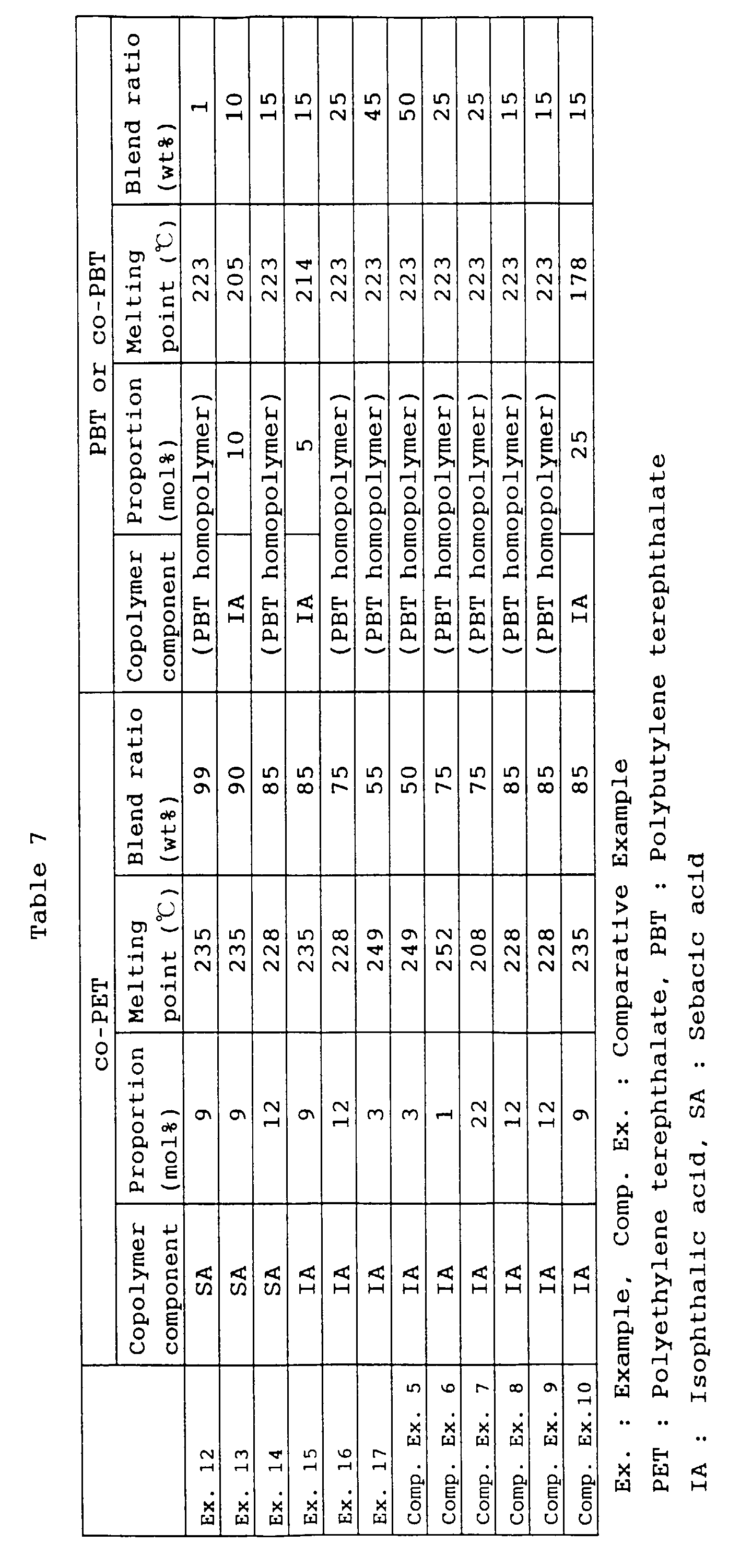

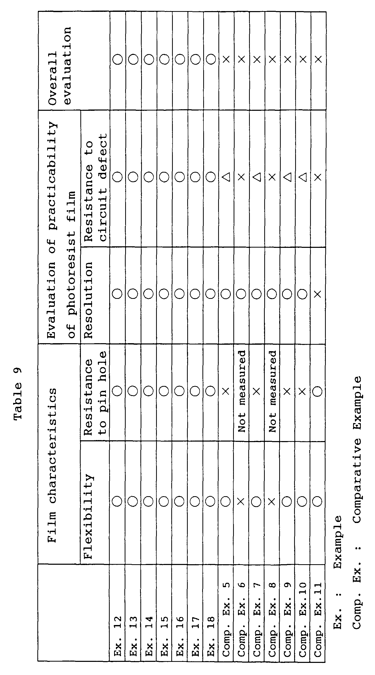
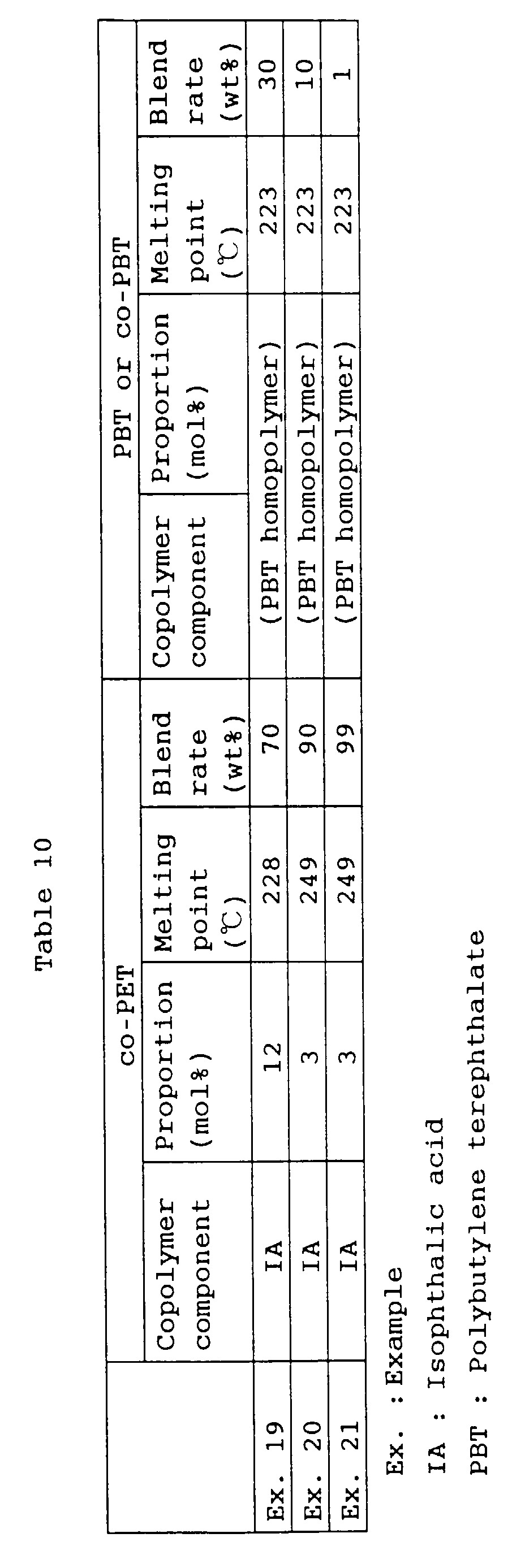


- As is evident from the results of Table 9 and Table 12, the films of Examples are all excellent in flexibility, resistance to pin hole, resolution and resistance to circuit defect.
- Copolyethylene terephthalate (to be referred to as polyester composition (I) hereinafter) containing 0.1 % by weight of spherical monodisperse silica (particle diameter ratio of 1.1) having an average particle size of 0.3 µm and a polyester composition (to be referred to as polyester composition (II) hereinafter) prepared by mixing a co-PET containing spherical monodisperse silica (particle diameter ratio of 1.07) having an average particle size of 1.5 µm and having, a copolymer component, components shown in Table 13 and PBT (homopolymer) in a blend ratio shown in Table 13 were separately molten at 280°C, coextruded from adjacent dies, laminated, thermally joined together and quenched to prepare an unstretched laminate film.
- Thereafter, this unstretched film was stretched to 3.2 times in a longitudinal direction at 105°C and to 3.4 times in a transverse direction at 110°C, and heat-set at 180°C to obtain a biaxially oriented laminate film having a thickness of 10 µm. At this point, a layer of the polyester composition (I) had a thickness of 2 µm and a layer of the polyester composition (II) had a thickness of 8 µm. The properties of this film are shown in Table 14.
- Further, a photoresist layer was formed on the side of the layer of the polyester composition (II) of this film and evaluation on the practicability of a photoresist film laminate was carried out in the same manner as in Example 1. The results are shown in Table 14.
- The procedure of Example 22 was repeated except that the PBT was replaced with a copolybutylene terephthalate containing a copolymer component shown in Table 13 and the blend ratio was changed as shown in Table 13. The results are shown in Table 14.


Claims (14)
- A photoresist film laminate consisting of (1) a protective film, (2) a photoresist layer and (3) a photoresist layer supporting film, which are laminated in order of mention, wherein said photoresist layer supporting film (A) is formed from a polymer composition comprising (i) 55 to 100 % by weight of a copolyester containing ethylene terephthalate units as a main recurring unit and having a melting point of 210 to 250°C and (ii) 0 to 45 % by weight of polybutylene terephthalate or a copolyester containing butylene terephthalate units as a main recurring unit and having a melting point of not lower than 180°C, and (B) has a plane orientation coefficient of 0.08 to 0.16.
- A laminate as claimed in claim 1, wherein the polymer composition contains 0.001 to 0.5 % by weight of a lubricant having an average particle size of not more than 2.5 µm.
- A laminate as claimed in claim 1 wherein the layer supporting film has L5 values in the longitudinal and transverse directions in the range of 1 to 65 g/mm, the L5 value being obtained in a tensile test carried out on a 10 mm wide strip-like sample of film.
- A laminate as claimed in claim 1 wherein the layer supporting film has a plane orientation coefficient of 0.10 to 0.15.
- A laminate as claimed in claim 1 wherein the layer supporting film has a thickness of 3 to 75 µm.
- A laminate as claimed in claim 1, wherein the polymer composition is a copolyester containing ethylene terephthalate as a main recurring unit and having a melting point of 215 to 235°C.
- A laminate as claimed in claim 1, wherein the polymer composition comprises (i) 55 to 99 % by weight of a copolyester containing ethylene terephthalate units as a main recurring unit and having a melting point of 210 to 250°C and (ii) 1 to 45 % by weight of polybutylene terephthalate or a copolyester containing butylene terephthalate units as a main recurring unit and having a melting point of not lower than 180°C.
- A photoresist film laminate consisting of (i) a photoresist layer supporting film, (ii) a photoresist layer and (iii) a conductive substrate, which are laminated in order of mention, wherein said photoresist layer supporting film (A) is formed from a polymer composition comprising (i) 55 to 100 % by weight of a copolyester containing ethylene terephthalate units as a main recurring unit and having a melting point of 210 to 250°C and (ii) 0 to 45 % by weight of polybutylene terephthalate or a copolyester containing butylene terephthalate units as a main recurring unit and having a melting point of not lower than 180°C, and (B) has a plane orientation coefficient of 0.08 to 0.16.
- The photoresist film laminate of claim 8, wherein the polymer composition contains 0.001 to 0.5 % by weight of a lubricant having an average particle size of not more than 2.5 µm.
- The photoresist film laminate of claim 8, in which the layer supporting film has L5 values in the longitudinal and transverse directions in the range of 1 to 65 g/mm, the L5 value being obtained in a tensile test carried out on a 10 mm wide strip-like sample of film.
- The photoresist film laminate of claim 8, in which the layer supporting film has a plane orientation coefficient of 0.10 to 0.15.
- The photoresist film laminate of claim 8, in which the layer supporting film has a thickness of 3 to 75 µm.
- The photoresist film laminate of claim 8, wherein the polymer composition is a copolyester containing ethylene terephthalate as a main recurring unit and having a melting point of 215 to 235°C.
- The photoresist film laminate of claim 8, wherein the polymer composition comprises (i) 55 to 99 % by weight of a copolyester containing ethylene terephthalate units as a main recurring unit and having a melting point of 210 to 250°C and (ii) 1 to 45 % by weight of polybutylene terephthalate or a copolyester containing butylene terephthalate units as a main recurring unit and having a melting point of not lower than 180°C.
Priority Applications (1)
| Application Number | Priority Date | Filing Date | Title |
|---|---|---|---|
| EP99202486A EP0961173B1 (en) | 1996-05-20 | 1997-05-12 | Photoresist layer supporting film |
Applications Claiming Priority (6)
| Application Number | Priority Date | Filing Date | Title |
|---|---|---|---|
| JP12457796 | 1996-05-20 | ||
| JP12457696 | 1996-05-20 | ||
| JP124577/96 | 1996-05-20 | ||
| JP12457796A JP3364380B2 (en) | 1996-05-20 | 1996-05-20 | Polyester film |
| JP124576/96 | 1996-05-20 | ||
| JP12457696A JP3150902B2 (en) | 1996-05-20 | 1996-05-20 | Polyester film |
Related Child Applications (1)
| Application Number | Title | Priority Date | Filing Date |
|---|---|---|---|
| EP99202486A Division EP0961173B1 (en) | 1996-05-20 | 1997-05-12 | Photoresist layer supporting film |
Publications (2)
| Publication Number | Publication Date |
|---|---|
| EP0809151A1 EP0809151A1 (en) | 1997-11-26 |
| EP0809151B1 true EP0809151B1 (en) | 2000-10-11 |
Family
ID=26461248
Family Applications (2)
| Application Number | Title | Priority Date | Filing Date |
|---|---|---|---|
| EP97303214A Expired - Lifetime EP0809151B1 (en) | 1996-05-20 | 1997-05-12 | Laminate of a photoresist layer supporting film and photoresist |
| EP99202486A Expired - Lifetime EP0961173B1 (en) | 1996-05-20 | 1997-05-12 | Photoresist layer supporting film |
Family Applications After (1)
| Application Number | Title | Priority Date | Filing Date |
|---|---|---|---|
| EP99202486A Expired - Lifetime EP0961173B1 (en) | 1996-05-20 | 1997-05-12 | Photoresist layer supporting film |
Country Status (5)
| Country | Link |
|---|---|
| US (2) | US5994027A (en) |
| EP (2) | EP0809151B1 (en) |
| KR (1) | KR100287237B1 (en) |
| DE (2) | DE69715676T2 (en) |
| TW (1) | TW477916B (en) |
Families Citing this family (5)
| Publication number | Priority date | Publication date | Assignee | Title |
|---|---|---|---|---|
| DE69715676T2 (en) * | 1996-05-20 | 2003-05-22 | Teijin Ltd., Osaka | Photoresist film |
| KR100370557B1 (en) * | 1998-10-27 | 2003-03-17 | 에스케이씨 주식회사 | Polyester film for base film of photoresist film |
| TW403952B (en) * | 1998-11-26 | 2000-09-01 | United Microelectronics Corp | The method of removing the photoresist |
| EP1114733B1 (en) * | 1999-06-01 | 2007-08-08 | Teijin Limited | Polyester film for ink image receiving substrate and ink image receiving substrate |
| KR100687984B1 (en) | 2003-09-05 | 2007-02-27 | 주식회사 코오롱 | Low Volatility Aromatic Polyester Resin Composition |
Family Cites Families (8)
| Publication number | Priority date | Publication date | Assignee | Title |
|---|---|---|---|---|
| JPS566498A (en) * | 1979-06-26 | 1981-01-23 | Hitachi Chemical Co Ltd | Method of manufacturing flexible printed circuit board |
| JPH07106394B2 (en) * | 1989-05-17 | 1995-11-15 | 東洋製罐株式会社 | Squeeze ironing can manufacturing method |
| JP3016943B2 (en) * | 1992-02-12 | 2000-03-06 | 帝人株式会社 | Polyester film for laminating metal plates |
| EP0576682B1 (en) * | 1992-01-16 | 1998-09-02 | Teijin Limited | Polyester film for metal sheet lamination and use thereof |
| EP0580404B1 (en) * | 1992-07-22 | 1999-09-15 | Teijin Limited | Biaxially oriented laminated polyester film for use as film to be bonded onto metal sheet |
| WO1995015993A1 (en) * | 1993-12-10 | 1995-06-15 | Teijin Limited | Transparent film for lamination coating of metallic can |
| JPH0996907A (en) * | 1995-10-02 | 1997-04-08 | Tamapori Kk | Photosensitive film |
| DE69715676T2 (en) * | 1996-05-20 | 2003-05-22 | Teijin Ltd., Osaka | Photoresist film |
-
1997
- 1997-05-12 DE DE69715676T patent/DE69715676T2/en not_active Expired - Fee Related
- 1997-05-12 EP EP97303214A patent/EP0809151B1/en not_active Expired - Lifetime
- 1997-05-12 EP EP99202486A patent/EP0961173B1/en not_active Expired - Lifetime
- 1997-05-12 DE DE69703264T patent/DE69703264T2/en not_active Expired - Fee Related
- 1997-05-13 US US08/855,468 patent/US5994027A/en not_active Expired - Fee Related
- 1997-05-19 TW TW086106641A patent/TW477916B/en not_active IP Right Cessation
- 1997-05-20 KR KR1019970019585A patent/KR100287237B1/en not_active Expired - Fee Related
-
1999
- 1999-04-27 US US09/299,651 patent/US6140013A/en not_active Expired - Fee Related
Also Published As
| Publication number | Publication date |
|---|---|
| US5994027A (en) | 1999-11-30 |
| EP0961173A1 (en) | 1999-12-01 |
| US6140013A (en) | 2000-10-31 |
| EP0961173B1 (en) | 2002-09-18 |
| DE69715676D1 (en) | 2002-10-24 |
| EP0809151A1 (en) | 1997-11-26 |
| DE69715676T2 (en) | 2003-05-22 |
| KR970074833A (en) | 1997-12-10 |
| TW477916B (en) | 2002-03-01 |
| KR100287237B1 (en) | 2001-04-16 |
| DE69703264T2 (en) | 2001-05-17 |
| DE69703264D1 (en) | 2000-11-16 |
Similar Documents
| Publication | Publication Date | Title |
|---|---|---|
| JP7000677B2 (en) | Polyester film | |
| KR20230079513A (en) | Biaxially oriented polyester film | |
| KR20030031164A (en) | Image display screen and image display unit | |
| JP2017186510A (en) | Polyester film | |
| EP0809151B1 (en) | Laminate of a photoresist layer supporting film and photoresist | |
| JP4269389B2 (en) | Polyester film for photoresist for extra fine wires | |
| KR101569552B1 (en) | Optical multilayer film | |
| JP2009178908A (en) | Release film | |
| JP2004174788A (en) | Biaxially oriented laminated polyester film | |
| JP2007056091A (en) | Polyester film and release film | |
| JP3364380B2 (en) | Polyester film | |
| JP3150902B2 (en) | Polyester film | |
| JP5123823B2 (en) | Optical laminated film | |
| JP2003327719A (en) | Polyester film for release film | |
| JP2004361446A (en) | Polyester film for photoresist | |
| JP5014616B2 (en) | Optical laminated polyester film | |
| JP2009204754A (en) | Release film for liquid crystal polarizing plate | |
| JP2009178930A (en) | Release film | |
| JP2000094507A (en) | Polyester film | |
| KR20200133723A (en) | Functional absence | |
| JP2009046567A (en) | Polyester film | |
| JP2023037175A (en) | Polyester film, miniature led substrate, backlight and display | |
| JP2003177542A (en) | Polyester film | |
| WO2022210249A1 (en) | Polyester film for protection of polarizer, and polarizing plate using same | |
| JP2012237853A (en) | Uniaxially stretched multilayer laminated film |
Legal Events
| Date | Code | Title | Description |
|---|---|---|---|
| PUAI | Public reference made under article 153(3) epc to a published international application that has entered the european phase |
Free format text: ORIGINAL CODE: 0009012 |
|
| AK | Designated contracting states |
Kind code of ref document: A1 Designated state(s): DE FR GB |
|
| 17P | Request for examination filed |
Effective date: 19980220 |
|
| 17Q | First examination report despatched |
Effective date: 19990204 |
|
| GRAG | Despatch of communication of intention to grant |
Free format text: ORIGINAL CODE: EPIDOS AGRA |
|
| RTI1 | Title (correction) |
Free format text: LAMINATE OF A PHOTORESIST LAYER SUPPORTING FILM AND PHOTORESIST |
|
| RTI1 | Title (correction) |
Free format text: LAMINATE OF A PHOTORESIST LAYER SUPPORTING FILM AND PHOTORESIST |
|
| GRAG | Despatch of communication of intention to grant |
Free format text: ORIGINAL CODE: EPIDOS AGRA |
|
| GRAH | Despatch of communication of intention to grant a patent |
Free format text: ORIGINAL CODE: EPIDOS IGRA |
|
| GRAH | Despatch of communication of intention to grant a patent |
Free format text: ORIGINAL CODE: EPIDOS IGRA |
|
| GRAA | (expected) grant |
Free format text: ORIGINAL CODE: 0009210 |
|
| AK | Designated contracting states |
Kind code of ref document: B1 Designated state(s): DE FR GB |
|
| REF | Corresponds to: |
Ref document number: 69703264 Country of ref document: DE Date of ref document: 20001116 |
|
| ET | Fr: translation filed | ||
| PLBE | No opposition filed within time limit |
Free format text: ORIGINAL CODE: 0009261 |
|
| STAA | Information on the status of an ep patent application or granted ep patent |
Free format text: STATUS: NO OPPOSITION FILED WITHIN TIME LIMIT |
|
| 26N | No opposition filed | ||
| REG | Reference to a national code |
Ref country code: GB Ref legal event code: IF02 |
|
| PGFP | Annual fee paid to national office [announced via postgrant information from national office to epo] |
Ref country code: GB Payment date: 20050425 Year of fee payment: 9 |
|
| PGFP | Annual fee paid to national office [announced via postgrant information from national office to epo] |
Ref country code: FR Payment date: 20050426 Year of fee payment: 9 |
|
| PGFP | Annual fee paid to national office [announced via postgrant information from national office to epo] |
Ref country code: DE Payment date: 20050609 Year of fee payment: 9 |
|
| PG25 | Lapsed in a contracting state [announced via postgrant information from national office to epo] |
Ref country code: GB Free format text: LAPSE BECAUSE OF NON-PAYMENT OF DUE FEES Effective date: 20060512 |
|
| PG25 | Lapsed in a contracting state [announced via postgrant information from national office to epo] |
Ref country code: DE Free format text: LAPSE BECAUSE OF NON-PAYMENT OF DUE FEES Effective date: 20061201 |
|
| GBPC | Gb: european patent ceased through non-payment of renewal fee |
Effective date: 20060512 |
|
| REG | Reference to a national code |
Ref country code: FR Ref legal event code: ST Effective date: 20070131 |
|
| PG25 | Lapsed in a contracting state [announced via postgrant information from national office to epo] |
Ref country code: FR Free format text: LAPSE BECAUSE OF NON-PAYMENT OF DUE FEES Effective date: 20060531 |