EP0808083B1 - Schaltungsanordnung zum Betreiben einer Last und elektronisches Vorschaltgerät mit einer derartigen Schaltungsanordnung zum Betreiben einer Lampe - Google Patents
Schaltungsanordnung zum Betreiben einer Last und elektronisches Vorschaltgerät mit einer derartigen Schaltungsanordnung zum Betreiben einer Lampe Download PDFInfo
- Publication number
- EP0808083B1 EP0808083B1 EP97106836A EP97106836A EP0808083B1 EP 0808083 B1 EP0808083 B1 EP 0808083B1 EP 97106836 A EP97106836 A EP 97106836A EP 97106836 A EP97106836 A EP 97106836A EP 0808083 B1 EP0808083 B1 EP 0808083B1
- Authority
- EP
- European Patent Office
- Prior art keywords
- switch
- inductance
- circuit
- load
- lamp
- Prior art date
- Legal status (The legal status is an assumption and is not a legal conclusion. Google has not performed a legal analysis and makes no representation as to the accuracy of the status listed.)
- Expired - Lifetime
Links
- 239000003990 capacitor Substances 0.000 claims abstract description 16
- 230000008878 coupling Effects 0.000 claims description 5
- 238000010168 coupling process Methods 0.000 claims description 5
- 238000005859 coupling reaction Methods 0.000 claims description 5
- 230000005669 field effect Effects 0.000 claims description 2
- 238000001914 filtration Methods 0.000 claims 2
- 230000001131 transforming effect Effects 0.000 claims 1
- 230000008901 benefit Effects 0.000 description 6
- 238000005516 engineering process Methods 0.000 description 3
- 238000011161 development Methods 0.000 description 1
- 230000018109 developmental process Effects 0.000 description 1
- 239000003792 electrolyte Substances 0.000 description 1
- 238000000034 method Methods 0.000 description 1
Images
Classifications
-
- H—ELECTRICITY
- H05—ELECTRIC TECHNIQUES NOT OTHERWISE PROVIDED FOR
- H05B—ELECTRIC HEATING; ELECTRIC LIGHT SOURCES NOT OTHERWISE PROVIDED FOR; CIRCUIT ARRANGEMENTS FOR ELECTRIC LIGHT SOURCES, IN GENERAL
- H05B41/00—Circuit arrangements or apparatus for igniting or operating discharge lamps
- H05B41/14—Circuit arrangements
- H05B41/26—Circuit arrangements in which the lamp is fed by power derived from DC by means of a converter, e.g. by high-voltage DC
- H05B41/28—Circuit arrangements in which the lamp is fed by power derived from DC by means of a converter, e.g. by high-voltage DC using static converters
-
- H—ELECTRICITY
- H02—GENERATION; CONVERSION OR DISTRIBUTION OF ELECTRIC POWER
- H02M—APPARATUS FOR CONVERSION BETWEEN AC AND AC, BETWEEN AC AND DC, OR BETWEEN DC AND DC, AND FOR USE WITH MAINS OR SIMILAR POWER SUPPLY SYSTEMS; CONVERSION OF DC OR AC INPUT POWER INTO SURGE OUTPUT POWER; CONTROL OR REGULATION THEREOF
- H02M3/00—Conversion of DC power input into DC power output
- H02M3/005—Conversion of DC power input into DC power output using Cuk converters
Definitions
- the present invention relates to a circuit arrangement according to the preamble of Claim 1 for operating a load and an electronic ballast with a such a circuit arrangement for operating a to the circuit arrangement connectable lamp, in particular a gas discharge lamp.
- the invention relates to converter circuits for use in electronic ballasts are suitable for controlling lamps.
- a well-known converter circuit is the so-called buck-boost converter.
- a corresponding circuit is shown in Fig. 3a.
- the buck-boost converter circuit comprises a coil L and an electrolytic capacitor C connected to the coil L via a diode D. Furthermore, a controllable switch S is provided which can be opened and closed as desired.
- a load R L can be connected in parallel to the capacitor C.
- a (half-wave) rectified input voltage U e is present at the input connections 1, 2 of the converter circuit. If the switch S is closed, current flows through the coil L, while with an open switch S no current can flow, so that - as shown in FIG. 3b - a sawtooth-shaped current profile i e (t) with interruptions due to the switching times of the switch S.
- t e corresponds to the switch-on time of the switches S and T to the period interval of the switch-on process.
- Fig. 3c it can be seen that the amplitude of the saw teeth of i e (t) approximates the course of the half wave of the input voltage U e .
- a half-wave of the sinusoidal input voltage U e thus represents the envelope for the amplitude of i e (t).
- the aim is that the amplitude of the input current i e (t) with the Input voltage U e or the mains voltage runs completely in phase.
- the buck-boost converter is a combination of a so-called buck converter and a boost converter. With a buck converter, it must always be ensured that the input voltage U e is higher than the output voltage U a applied to the load R L , In contrast, the voltage relationships required for a boost converter are reversed.
- the buck-boost converter has the advantage that both voltage ratios are possible. It is therefore also possible with the buck-boost converter that the input voltage is the same as the output voltage.
- the choice of the ratio of the input voltage U e to the output voltage U a is made via the pulse duty factor of the switch S, ie by changing the switch-on time t e of the switch S.
- a buck-boost converter circuit for operating a gas discharge lamp is described in EP-A1- 0 642 295 of the applicant.
- the buck-boost converter circuit has the disadvantage, however, that interruptions occur between the individual saw teeth of the current profile i e (t), due to which harmonics are generated which are reflected back into the network and thus have to be filtered out specifically.
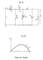
- SEPIC S ingle E nded P rimary I nductance C onverter
- the circuit comprises a series circuit consisting of an inductor L1 and a switch S1 and a charging capacitor C1 which is connected in parallel with the switch S1 with a further inductor L2.
- the two inductors are coupled to one another in such a way that the mutually induced voltages do not cancel each other out.
- the degree of coupling between the two inductors L1 and L2 is a measure of the approximation of the input current i e (t) to the envelope of the input voltage U e and thus represents, in addition to the duty cycle of the switch S1, an additional parameter for varying the circuit properties.
- the one to be operated Load R L can be connected in parallel to a further (electrolyte) capacitor C2, the capacitor C2 being connected in parallel via a diode D to the second inductor or coil L2.
- the operation of the circuit shown in FIG. 4a is as follows: if the switch S1 is open and the charging capacitor C1 is charged, current flows through L1, C1 and L2 regardless of the open switch S1. If the switch S1 is closed, current continues to flow as with the buck-boost converter. In addition, however, current also flows via L2, D and the parallel connection from R L and C2. Since the inductors L1 and L2 are coupled to one another, an energy field builds up in the first coil L1, which again provides the current flow via C1 and L2 when the switch S1 is opened.
- the SEPIC circuit thus has the advantage that regardless of whether the switch S1 1 is open or closed, current always flows, so that the interruptions or pauses between the individual saw teeth of the current profile i e (t) are eliminated.
- 4b shows the time course of the input current i e (t) in relation to the envelope of the input voltage Ue. It can be seen that the course of the input current i e (t) with a small ripple is closely approximated to the envelope of the input voltage U e and the interruptions between the individual saw teeth of i e (t) are eliminated.
- the present invention is based on the SEPIC circuit shown in FIG. 4a the task of further developing this circuit arrangement in such a way that maintaining the benefits of SEPIC technology for operating a lamp, is particularly suitable in an electronic ballast.
- the diode shown in Fig. 4a by a second switch replaced and the lamp to be operated as a load is parallel to this second switch can be connected.
- the invention comprises Circuit arrangement in parallel with the second switch a load circuit with a Series resonance circuit for controlling a (gas discharge) lamp to be connected to it.
- the circuit arrangement according to the present invention has the advantage that them without problems in ordinary electronic ballasts for driving Lamps can be used.
- By alternately switching the two switches of the Circuit arrangement flows in the output-side load circuit of the circuit arrangement synchronously with the switching between the switches alternately a current in reverse direction.
- the circuit arrangement according to the invention thus acts as one Inverters required for the operation of gas discharge lamps low-frequency mains alternating voltage into a high-frequency lamp voltage converted to avoid flickering of the connected lamp or lamps, however, the circuit arrangement according to the invention with very few Circuit elements gets along.
- SEPIC technology are preserved, i.e. Interruptions between the saw teeth of the input current profile are avoided so that no harmonics can occur due to these interruptions.
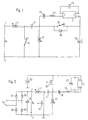
- Fig. 1 shows a preferred embodiment of the invention Circuitry. Since the operation of the circuit shown in Fig. 1 largely corresponds to that of the circuit shown in FIG. 4a only the differences are discussed below.
- the diode shown in FIG. 4 is replaced by a second switch S2.
- a load circuit for a lamp 3 to be connected thereto, in particular for a gas discharge lamp, is arranged parallel to this second switch S2.
- the load circuit comprises a series resonance circuit with a further inductance L3 and a further capacitance C3. If a lamp 3 is connected to the circuit arrangement, the coil L3 is in series with the lamp, while the capacitor C3 is arranged in parallel with the lamp.
- the series resonance circuit is used to ignite the lamp by bringing the frequency of the input voltage U e close to the resonance frequency of the series resonance circuit. An ignited lamp can be dimmed by removing the frequency of the input voltage from the resonance frequency.
- a free-wheeling diode D5 is advantageously connected in parallel with the second switch S2 in order to protect it from overvoltages of wrong polarity.
- the lamp 3 thus corresponds to the load R L shown in general form in FIG. 4a.
- FIG. 2 shows an electronic ballast with the circuit arrangement shown in FIG. 1.
- the electronic ballast comprises a bridge rectifier circuit, consisting of diodes D1-D4, which is fed on the input side with the mains voltage.
- any rectifier circuit can be used which can convert the mains voltage into a half-wave rectified input voltage U e for the circuit arrangement according to the invention.
- the rectifier circuit is connected to the circuit arrangement according to the present invention, a further capacitor C5 being additionally present between the input connections 1, 2 of the circuit arrangement, which capacitor is not used to smooth the sine half-waves of the half-wave rectified input voltage U e of the converter circuit according to the invention, but only to filter out the harmonics generated by switching switches S1 and S2.
- the capacitor C2 connected to the load circuit of the lamp 3 is connected to the second inductance L2 and the first switch S1 via a ground connection.
- the two switches S1 and S2 are designed as MOS field-effect transistors and can be switched on and off, ie opened and closed, by applying a corresponding control voltage to their gate connections.
- the two switches S1 and S2 are switched alternately, so that on the output side the lamp 3 a high-frequency AC voltage for operating the lamp 3 occurs because a current in the load circuit synchronously with the switching of the switches S1 and S2 flows in the opposite direction.
- the circuit arrangement shown in FIGS. 1 and 2 acts thus like an ordinary inverter, but by using the SEPIC technology due to interruptions between the saw teeth of the Harmonics generated in the input current can be avoided and very few Circuit elements must be used.
Landscapes
- Circuit Arrangements For Discharge Lamps (AREA)
- Engineering & Computer Science (AREA)
- Power Engineering (AREA)
Description
Claims (13)
- Schaltungsanordnung zum Umwandeln einer gleichgerichteten Eingangsspannung (Ue) in eine Ausgangs-Wechselspannung (Ua) zum Betreiben einer an die Schaltungsanordnung anschließbaren Last (RL; 3),
mit einer an einen ersten Eingangsanschluß (1) angeschlossenen ersten Induktivität (L1) und einem zwischen die erste Induktivität (L1) und einen zweiten Eingangsanschluß (2) geschalteten ersten steuerbaren Schalter (S1),
mit einer zu dem ersten Schalter (S1) parallelgeschalteten Serienschaltung aus einer ersten Kapazität (C1) und einer zweiten Induktivität (L2), die mit der ersten Induktivität (L1) gekoppelt ist, und
mit einer über ein weiteres Schaltungselement (S2) zu der zweiten Induktivität (L2) parallelgeschalteten zweiten Kapazität (C2),
dadurch gekennzeichnet, daß das weitere Schaltungselement ein zweiter steuerbarer Schalter (S2) ist, wobei die beiden Schalter (S1, S2) zur Erzeugung der Ausgangs-Wechselspannung (Ua) wechselseitig geschlossen bzw. geöffnet werden können und die Last (RL; 3) parallel zu dem zweiten Schalter (S2) anschließbar ist. - Schaltungsanordnung nach Anspruch 1,
dadurch gekennzeichnet, daß die zweite Induktivität (L2) mit der ersten Induktivität (L1) derart gekoppelt ist, daß sich die durch die Induktivitäten (L1, L2) wechselseitig induzierten Spannungen nicht gegenseitig aufheben. - Schaltungsanordnung nach Ansprüche 1 order 2,
dadurch gekennzeichnet, daß der erste und zweite Schalter (S1, S2) steuerbare MOS-Feldeffekttransistoren sind. - Schaltungsanordnung nach einem der vorhergehenden Ansprüche,
dadurch gekennzeichnet, daß der Kopplungsgrad zwischen der ersten und zweiten Induktivität (L1, L2) und/oder das Tastverhältnis zwischen den Einschaltzeiten des ersten und zweiten Schalters (S1, S2) und/oder die Einschaltfrequenz des ersten und zweiten Schalters (S1, S2) variierbar ist. - Schaltungsanordnung nach einem der vorhergehenden Ansprüche,
dadurch gekennzeichnet, daß eine Diode (D5) zu dem zweiten Schalter (S2) parallelgeschaltet ist. - Schaltungsanordnung nach einem der vorhergehenden Ansprüche,
dadurch gekennzeichnet, daß ein Lastkreis (C3, L3, C4), an den die Last (RL, 3) anschließbar ist, parallel zu dem zweiten Schalter (S2) angeordnet ist. - Schaltungsanordnung nach Anspruch 6,
dadurch gekennzeichnet, daß der Lastkreis einen Serienresonanzkreis aus einer dritten Kapazität (C3) und einer dritten Induktivität (L3) urnfaßt. - Schaltungsanordnung nach Anspruch 7,
dadurch gekennzeichnet, daß der Lastkreis eine mit der dritten Induktivität (L3) in Serie geschaltete vierte Kapazität (C4) als Koppelkondensator umfaßt. - Elektronischen Vorschaltgerät zum Betreiben einer Lampe (3) mit einer Schaltungsanordnung nach einem der vorhergehenden Ansprüche,
dadurch gekennzeichnet, daß die Lampe (3) als die Last an die Schaltungsanordnung anschließbar ist. - Elektronisches Vorschaltgerät nach Anspruch 9 mit einer Schaltungsanordnung nach Anspruch 7 oder 8,
dadurch gekennzeichnet, daß die dritte Kapazität (C3) zu der Lampe (3) parallel und die dritte Induktivität (L3) zu der Lampe (3) in Serie geschaltet ist. - Elektronisches Vorschaltgerät nach Anspruch 9 oder 10,
dadurch gekennzeichnet, daß die Eingangsanschlüsse (1, 2) der Schaltungsanordnung mit einer Gleichrichterschaltung (D1 - D4) verbunden sind, die von einer Netzspannung (UN) gespeist wird. - Elektronisches Vorschaltgerät nach einem der Ansprüche 9 bis 11,
gekennzeichnet durch
eine Vorrichtung (C5) zum Ausfiltern von Oberwellen. - Elektronisches Vorschaltgerät nach Anspruch 12,
dadurch gekennzeichnet, daß die Vorrichtung zum Ausfiltern von Oberwellen durch einen zwischen die Eingangsanschlüsse (1, 2) der Schaltungsanordnung geschalteten Filterkondensator (C5) gebildet ist.
Applications Claiming Priority (2)
| Application Number | Priority Date | Filing Date | Title |
|---|---|---|---|
| DE19619745 | 1996-05-15 | ||
| DE19619745A DE19619745A1 (de) | 1996-05-15 | 1996-05-15 | Schaltungsanordnung zum Betreiben einer Last und elektronisches Vorschaltgerät mit einer derartigen Schaltungsanordnung zum Betreiben einer Lampe |
Publications (3)
| Publication Number | Publication Date |
|---|---|
| EP0808083A2 EP0808083A2 (de) | 1997-11-19 |
| EP0808083A3 EP0808083A3 (de) | 1998-12-23 |
| EP0808083B1 true EP0808083B1 (de) | 2003-09-24 |
Family
ID=7794472
Family Applications (1)
| Application Number | Title | Priority Date | Filing Date |
|---|---|---|---|
| EP97106836A Expired - Lifetime EP0808083B1 (de) | 1996-05-15 | 1997-04-24 | Schaltungsanordnung zum Betreiben einer Last und elektronisches Vorschaltgerät mit einer derartigen Schaltungsanordnung zum Betreiben einer Lampe |
Country Status (3)
| Country | Link |
|---|---|
| EP (1) | EP0808083B1 (de) |
| AT (1) | ATE250822T1 (de) |
| DE (2) | DE19619745A1 (de) |
Families Citing this family (2)
| Publication number | Priority date | Publication date | Assignee | Title |
|---|---|---|---|---|
| DE10210804B4 (de) * | 2002-03-12 | 2004-05-27 | B & S Elektronische Geräte GmbH | Vorschaltgerät für eine Entladungslampe |
| CN102695345B (zh) * | 2012-06-01 | 2014-03-26 | 雷锡社 | 能效型智能镇流器 |
Family Cites Families (7)
| Publication number | Priority date | Publication date | Assignee | Title |
|---|---|---|---|---|
| DE3301632A1 (de) * | 1983-01-19 | 1984-07-26 | Siemens AG, 1000 Berlin und 8000 München | Umrichter |
| DE3923311A1 (de) * | 1989-07-14 | 1991-01-24 | Datron Electronic Gmbh | Elektrischer wandler |
| EP0596152B1 (de) * | 1992-11-06 | 1998-06-10 | TRILUX-LENZE GmbH & Co. KG | Wechselspannungs-Vorschaltgerät für elektrische Entladungslampen |
| DE4329821A1 (de) * | 1993-09-03 | 1995-03-09 | Tridonic Bauelemente Ges Mbh | Elektronisches Vorschaltgerät zum Versorgen einer Last, beispielsweise einer Lampe |
| US5416387A (en) * | 1993-11-24 | 1995-05-16 | California Institute Of Technology | Single stage, high power factor, gas discharge lamp ballast |
| US5583421A (en) * | 1994-08-10 | 1996-12-10 | Hewlett-Packard Company | Sepic converter with transformerless line isolation |
| DE4446532A1 (de) * | 1994-12-24 | 1996-06-27 | Bosch Gmbh Robert | Stromversorgungsschaltung |
-
1996
- 1996-05-15 DE DE19619745A patent/DE19619745A1/de not_active Withdrawn
-
1997
- 1997-04-24 DE DE59710766T patent/DE59710766D1/de not_active Expired - Lifetime
- 1997-04-24 AT AT97106836T patent/ATE250822T1/de not_active IP Right Cessation
- 1997-04-24 EP EP97106836A patent/EP0808083B1/de not_active Expired - Lifetime
Also Published As
| Publication number | Publication date |
|---|---|
| ATE250822T1 (de) | 2003-10-15 |
| EP0808083A2 (de) | 1997-11-19 |
| EP0808083A3 (de) | 1998-12-23 |
| DE19619745A1 (de) | 1997-11-20 |
| DE59710766D1 (de) | 2003-10-30 |
Similar Documents
| Publication | Publication Date | Title |
|---|---|---|
| DE69509459T2 (de) | Hochfrequenter wechselstromwandler mit leistungsfaktorkorrektur | |
| EP1369985B1 (de) | Wechselrichter zum Umwandeln einer elektrischen Gleichspannung in einen Wechselstrom oder eine Wechselspannung | |
| DE102004030912B3 (de) | Verfahren zum Umwandeln einer elektrischen Gleichspannung einer Gleichspannungsquelle, insbesondere einer Photovoltaik-Gleichspannungsquelle in eine Wechselspannung | |
| EP2580858B1 (de) | Schaltungstopologie für einen phasenanschluss eines wechselrichters | |
| EP2144359A2 (de) | DC/DC- Wandler | |
| WO2009000465A1 (de) | Leistungsfaktor-korrekturschaltung für ein elektronisches vorschaltgerät für ein leuchtmittel | |
| DE69822126T2 (de) | Elektronisches vorschaltgerät mit parallelladung und reihensteuerung | |
| DE102017212462A1 (de) | Galvanisch gekoppelter elektrischer Wandler | |
| EP0439240A2 (de) | Elektronisches Vorschaltgerät | |
| EP0808085A2 (de) | Hochfrequenzbetriebsschaltung für eine Niederdruckentladungslampe mit verbesserter elektromagnetischer Verträglichkeit | |
| EP0808083B1 (de) | Schaltungsanordnung zum Betreiben einer Last und elektronisches Vorschaltgerät mit einer derartigen Schaltungsanordnung zum Betreiben einer Lampe | |
| DE102016224310A1 (de) | Hocheffizienter Stromrichter für einphasige Systeme | |
| DE69317751T2 (de) | Struktur eines statischen Frequenzumwandlers | |
| CH688066A5 (de) | Wechselstrom/Gleichstrom-Wandler nach dem Buck-/Boost-Prinzip. | |
| DE29622825U1 (de) | Bestrahlungsgerät | |
| EP0642295A1 (de) | Elektronisches Vorschaltgerät zum Versorgen einer Last, beispielsweise einer Lampe | |
| DE69313256T2 (de) | Ballastschaltung | |
| DE102015115481A1 (de) | Schaltnetzteilvorrichtung | |
| DE3020745C2 (de) | Fremdgesteuerter Gleichspannungswandler | |
| DE10012362B4 (de) | Elektronischer Transformator und Verfahren zum Betrieb mindestens einer Lampe | |
| EP0855849B1 (de) | Elektronischer Transformator | |
| DE10012363A1 (de) | Elektronischer Transformator | |
| WO2004015865A1 (de) | Schaltungsanordnung zur steuerung von zwei unabhangigen mit einer gleichgericht eten wechselspannung betreibbaren lasten | |
| DE202005013674U1 (de) | Potentialtrennung für SEPIC-Konverter | |
| AT503778B1 (de) | Vorrichtung zum steuern der spannungsversorgung eines verbrauchers, insbesondere einer beleuchtung |
Legal Events
| Date | Code | Title | Description |
|---|---|---|---|
| PUAI | Public reference made under article 153(3) epc to a published international application that has entered the european phase |
Free format text: ORIGINAL CODE: 0009012 |
|
| AK | Designated contracting states |
Kind code of ref document: A2 Designated state(s): AT BE CH DE ES FI FR GB IT LI NL SE |
|
| PUAL | Search report despatched |
Free format text: ORIGINAL CODE: 0009013 |
|
| AK | Designated contracting states |
Kind code of ref document: A3 Designated state(s): AT BE CH DE ES FI FR GB IT LI NL SE |
|
| RHK1 | Main classification (correction) |
Ipc: H02M 7/537 |
|
| 17P | Request for examination filed |
Effective date: 19990205 |
|
| 17Q | First examination report despatched |
Effective date: 19991005 |
|
| GRAG | Despatch of communication of intention to grant |
Free format text: ORIGINAL CODE: EPIDOS AGRA |
|
| GRAG | Despatch of communication of intention to grant |
Free format text: ORIGINAL CODE: EPIDOS AGRA |
|
| GRAH | Despatch of communication of intention to grant a patent |
Free format text: ORIGINAL CODE: EPIDOS IGRA |
|
| RAP1 | Party data changed (applicant data changed or rights of an application transferred) |
Owner name: TRIDONICATCO GMBH & CO. KG |
|
| GRAH | Despatch of communication of intention to grant a patent |
Free format text: ORIGINAL CODE: EPIDOS IGRA |
|
| GRAA | (expected) grant |
Free format text: ORIGINAL CODE: 0009210 |
|
| RIC1 | Information provided on ipc code assigned before grant |
Ipc: 7H 05B 41/28 B Ipc: 7H 02M 7/537 A |
|
| AK | Designated contracting states |
Kind code of ref document: B1 Designated state(s): AT BE CH DE ES FI FR GB IT LI NL SE |
|
| PG25 | Lapsed in a contracting state [announced via postgrant information from national office to epo] |
Ref country code: NL Free format text: LAPSE BECAUSE OF FAILURE TO SUBMIT A TRANSLATION OF THE DESCRIPTION OR TO PAY THE FEE WITHIN THE PRESCRIBED TIME-LIMIT Effective date: 20030924 Ref country code: IT Free format text: LAPSE BECAUSE OF FAILURE TO SUBMIT A TRANSLATION OF THE DESCRIPTION OR TO PAY THE FEE WITHIN THE PRESCRIBED TIME-LIMIT;WARNING: LAPSES OF ITALIAN PATENTS WITH EFFECTIVE DATE BEFORE 2007 MAY HAVE OCCURRED AT ANY TIME BEFORE 2007. THE CORRECT EFFECTIVE DATE MAY BE DIFFERENT FROM THE ONE RECORDED. Effective date: 20030924 Ref country code: GB Free format text: LAPSE BECAUSE OF FAILURE TO SUBMIT A TRANSLATION OF THE DESCRIPTION OR TO PAY THE FEE WITHIN THE PRESCRIBED TIME-LIMIT Effective date: 20030924 Ref country code: FR Free format text: LAPSE BECAUSE OF FAILURE TO SUBMIT A TRANSLATION OF THE DESCRIPTION OR TO PAY THE FEE WITHIN THE PRESCRIBED TIME-LIMIT Effective date: 20030924 Ref country code: FI Free format text: LAPSE BECAUSE OF FAILURE TO SUBMIT A TRANSLATION OF THE DESCRIPTION OR TO PAY THE FEE WITHIN THE PRESCRIBED TIME-LIMIT Effective date: 20030924 |
|
| REG | Reference to a national code |
Ref country code: GB Ref legal event code: FG4D Free format text: NOT ENGLISH |
|
| REG | Reference to a national code |
Ref country code: CH Ref legal event code: EP |
|
| REF | Corresponds to: |
Ref document number: 59710766 Country of ref document: DE Date of ref document: 20031030 Kind code of ref document: P |
|
| PG25 | Lapsed in a contracting state [announced via postgrant information from national office to epo] |
Ref country code: SE Free format text: LAPSE BECAUSE OF FAILURE TO SUBMIT A TRANSLATION OF THE DESCRIPTION OR TO PAY THE FEE WITHIN THE PRESCRIBED TIME-LIMIT Effective date: 20031224 |
|
| PG25 | Lapsed in a contracting state [announced via postgrant information from national office to epo] |
Ref country code: ES Free format text: LAPSE BECAUSE OF FAILURE TO SUBMIT A TRANSLATION OF THE DESCRIPTION OR TO PAY THE FEE WITHIN THE PRESCRIBED TIME-LIMIT Effective date: 20040104 |
|
| NLV1 | Nl: lapsed or annulled due to failure to fulfill the requirements of art. 29p and 29m of the patents act | ||
| GBV | Gb: ep patent (uk) treated as always having been void in accordance with gb section 77(7)/1977 [no translation filed] |
Effective date: 20030924 |
|
| PG25 | Lapsed in a contracting state [announced via postgrant information from national office to epo] |
Ref country code: BE Free format text: LAPSE BECAUSE OF NON-PAYMENT OF DUE FEES Effective date: 20040430 |
|
| PLBE | No opposition filed within time limit |
Free format text: ORIGINAL CODE: 0009261 |
|
| STAA | Information on the status of an ep patent application or granted ep patent |
Free format text: STATUS: NO OPPOSITION FILED WITHIN TIME LIMIT |
|
| 26N | No opposition filed |
Effective date: 20040625 |
|
| EN | Fr: translation not filed | ||
| BERE | Be: lapsed |
Owner name: *TRIDONICATCO G.M.B.H. & CO. K.G. Effective date: 20040430 |
|
| PGFP | Annual fee paid to national office [announced via postgrant information from national office to epo] |
Ref country code: AT Payment date: 20070423 Year of fee payment: 11 |
|
| REG | Reference to a national code |
Ref country code: CH Ref legal event code: PFA Owner name: TRIDONICATCO GMBH & CO. KG Free format text: TRIDONICATCO GMBH & CO. KG#FAERBERGASSE 15#6851 DORNBIRN (AT) -TRANSFER TO- TRIDONICATCO GMBH & CO. KG#FAERBERGASSE 15#6851 DORNBIRN (AT) |
|
| PG25 | Lapsed in a contracting state [announced via postgrant information from national office to epo] |
Ref country code: AT Free format text: LAPSE BECAUSE OF NON-PAYMENT OF DUE FEES Effective date: 20080424 |
|
| PGFP | Annual fee paid to national office [announced via postgrant information from national office to epo] |
Ref country code: DE Payment date: 20110629 Year of fee payment: 15 |
|
| PGFP | Annual fee paid to national office [announced via postgrant information from national office to epo] |
Ref country code: CH Payment date: 20120430 Year of fee payment: 16 |
|
| REG | Reference to a national code |
Ref country code: DE Ref legal event code: R119 Ref document number: 59710766 Country of ref document: DE Effective date: 20121101 |
|
| REG | Reference to a national code |
Ref country code: CH Ref legal event code: PL |
|
| PG25 | Lapsed in a contracting state [announced via postgrant information from national office to epo] |
Ref country code: CH Free format text: LAPSE BECAUSE OF NON-PAYMENT OF DUE FEES Effective date: 20130430 Ref country code: LI Free format text: LAPSE BECAUSE OF NON-PAYMENT OF DUE FEES Effective date: 20130430 |
|
| PG25 | Lapsed in a contracting state [announced via postgrant information from national office to epo] |
Ref country code: DE Free format text: LAPSE BECAUSE OF NON-PAYMENT OF DUE FEES Effective date: 20121101 |