EP0808083B1 - Circuit for operating a load and electronic ballast with such a circuit for operating a lamp - Google Patents
Circuit for operating a load and electronic ballast with such a circuit for operating a lamp Download PDFInfo
- Publication number
- EP0808083B1 EP0808083B1 EP97106836A EP97106836A EP0808083B1 EP 0808083 B1 EP0808083 B1 EP 0808083B1 EP 97106836 A EP97106836 A EP 97106836A EP 97106836 A EP97106836 A EP 97106836A EP 0808083 B1 EP0808083 B1 EP 0808083B1
- Authority
- EP
- European Patent Office
- Prior art keywords
- switch
- inductance
- circuit
- load
- lamp
- Prior art date
- Legal status (The legal status is an assumption and is not a legal conclusion. Google has not performed a legal analysis and makes no representation as to the accuracy of the status listed.)
- Expired - Lifetime
Links
- 239000003990 capacitor Substances 0.000 claims abstract description 16
- 230000008878 coupling Effects 0.000 claims description 5
- 238000010168 coupling process Methods 0.000 claims description 5
- 238000005859 coupling reaction Methods 0.000 claims description 5
- 230000005669 field effect Effects 0.000 claims description 2
- 238000001914 filtration Methods 0.000 claims 2
- 230000001131 transforming effect Effects 0.000 claims 1
- 230000008901 benefit Effects 0.000 description 6
- 238000005516 engineering process Methods 0.000 description 3
- 238000011161 development Methods 0.000 description 1
- 230000018109 developmental process Effects 0.000 description 1
- 239000003792 electrolyte Substances 0.000 description 1
- 238000000034 method Methods 0.000 description 1
Images
Classifications
-
- H—ELECTRICITY
- H05—ELECTRIC TECHNIQUES NOT OTHERWISE PROVIDED FOR
- H05B—ELECTRIC HEATING; ELECTRIC LIGHT SOURCES NOT OTHERWISE PROVIDED FOR; CIRCUIT ARRANGEMENTS FOR ELECTRIC LIGHT SOURCES, IN GENERAL
- H05B41/00—Circuit arrangements or apparatus for igniting or operating discharge lamps
- H05B41/14—Circuit arrangements
- H05B41/26—Circuit arrangements in which the lamp is fed by power derived from DC by means of a converter, e.g. by high-voltage DC
- H05B41/28—Circuit arrangements in which the lamp is fed by power derived from DC by means of a converter, e.g. by high-voltage DC using static converters
-
- H—ELECTRICITY
- H02—GENERATION; CONVERSION OR DISTRIBUTION OF ELECTRIC POWER
- H02M—APPARATUS FOR CONVERSION BETWEEN AC AND AC, BETWEEN AC AND DC, OR BETWEEN DC AND DC, AND FOR USE WITH MAINS OR SIMILAR POWER SUPPLY SYSTEMS; CONVERSION OF DC OR AC INPUT POWER INTO SURGE OUTPUT POWER; CONTROL OR REGULATION THEREOF
- H02M3/00—Conversion of DC power input into DC power output
- H02M3/005—Conversion of DC power input into DC power output using Cuk converters
Definitions
- the present invention relates to a circuit arrangement according to the preamble of Claim 1 for operating a load and an electronic ballast with a such a circuit arrangement for operating a to the circuit arrangement connectable lamp, in particular a gas discharge lamp.
- the invention relates to converter circuits for use in electronic ballasts are suitable for controlling lamps.
- a well-known converter circuit is the so-called buck-boost converter.
- a corresponding circuit is shown in Fig. 3a.
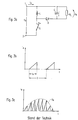
- the buck-boost converter circuit comprises a coil L and an electrolytic capacitor C connected to the coil L via a diode D. Furthermore, a controllable switch S is provided which can be opened and closed as desired.
- a load R L can be connected in parallel to the capacitor C.
- a (half-wave) rectified input voltage U e is present at the input connections 1, 2 of the converter circuit. If the switch S is closed, current flows through the coil L, while with an open switch S no current can flow, so that - as shown in FIG. 3b - a sawtooth-shaped current profile i e (t) with interruptions due to the switching times of the switch S.
- t e corresponds to the switch-on time of the switches S and T to the period interval of the switch-on process.
- Fig. 3c it can be seen that the amplitude of the saw teeth of i e (t) approximates the course of the half wave of the input voltage U e .
- a half-wave of the sinusoidal input voltage U e thus represents the envelope for the amplitude of i e (t).
- the aim is that the amplitude of the input current i e (t) with the Input voltage U e or the mains voltage runs completely in phase.
- the buck-boost converter is a combination of a so-called buck converter and a boost converter. With a buck converter, it must always be ensured that the input voltage U e is higher than the output voltage U a applied to the load R L , In contrast, the voltage relationships required for a boost converter are reversed.
- the buck-boost converter has the advantage that both voltage ratios are possible. It is therefore also possible with the buck-boost converter that the input voltage is the same as the output voltage.
- the choice of the ratio of the input voltage U e to the output voltage U a is made via the pulse duty factor of the switch S, ie by changing the switch-on time t e of the switch S.
- a buck-boost converter circuit for operating a gas discharge lamp is described in EP-A1- 0 642 295 of the applicant.
- the buck-boost converter circuit has the disadvantage, however, that interruptions occur between the individual saw teeth of the current profile i e (t), due to which harmonics are generated which are reflected back into the network and thus have to be filtered out specifically.
- SEPIC S ingle E nded P rimary I nductance C onverter
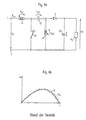
- the circuit comprises a series circuit consisting of an inductor L1 and a switch S1 and a charging capacitor C1 which is connected in parallel with the switch S1 with a further inductor L2.
- the two inductors are coupled to one another in such a way that the mutually induced voltages do not cancel each other out.
- the degree of coupling between the two inductors L1 and L2 is a measure of the approximation of the input current i e (t) to the envelope of the input voltage U e and thus represents, in addition to the duty cycle of the switch S1, an additional parameter for varying the circuit properties.
- the one to be operated Load R L can be connected in parallel to a further (electrolyte) capacitor C2, the capacitor C2 being connected in parallel via a diode D to the second inductor or coil L2.
- the operation of the circuit shown in FIG. 4a is as follows: if the switch S1 is open and the charging capacitor C1 is charged, current flows through L1, C1 and L2 regardless of the open switch S1. If the switch S1 is closed, current continues to flow as with the buck-boost converter. In addition, however, current also flows via L2, D and the parallel connection from R L and C2. Since the inductors L1 and L2 are coupled to one another, an energy field builds up in the first coil L1, which again provides the current flow via C1 and L2 when the switch S1 is opened.
- the SEPIC circuit thus has the advantage that regardless of whether the switch S1 1 is open or closed, current always flows, so that the interruptions or pauses between the individual saw teeth of the current profile i e (t) are eliminated.
- 4b shows the time course of the input current i e (t) in relation to the envelope of the input voltage Ue. It can be seen that the course of the input current i e (t) with a small ripple is closely approximated to the envelope of the input voltage U e and the interruptions between the individual saw teeth of i e (t) are eliminated.
- the present invention is based on the SEPIC circuit shown in FIG. 4a the task of further developing this circuit arrangement in such a way that maintaining the benefits of SEPIC technology for operating a lamp, is particularly suitable in an electronic ballast.
- the diode shown in Fig. 4a by a second switch replaced and the lamp to be operated as a load is parallel to this second switch can be connected.
- the invention comprises Circuit arrangement in parallel with the second switch a load circuit with a Series resonance circuit for controlling a (gas discharge) lamp to be connected to it.
- the circuit arrangement according to the present invention has the advantage that them without problems in ordinary electronic ballasts for driving Lamps can be used.
- By alternately switching the two switches of the Circuit arrangement flows in the output-side load circuit of the circuit arrangement synchronously with the switching between the switches alternately a current in reverse direction.
- the circuit arrangement according to the invention thus acts as one Inverters required for the operation of gas discharge lamps low-frequency mains alternating voltage into a high-frequency lamp voltage converted to avoid flickering of the connected lamp or lamps, however, the circuit arrangement according to the invention with very few Circuit elements gets along.
- SEPIC technology are preserved, i.e. Interruptions between the saw teeth of the input current profile are avoided so that no harmonics can occur due to these interruptions.
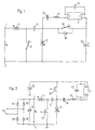
- Fig. 1 shows a preferred embodiment of the invention Circuitry. Since the operation of the circuit shown in Fig. 1 largely corresponds to that of the circuit shown in FIG. 4a only the differences are discussed below.
- the diode shown in FIG. 4 is replaced by a second switch S2.
- a load circuit for a lamp 3 to be connected thereto, in particular for a gas discharge lamp, is arranged parallel to this second switch S2.
- the load circuit comprises a series resonance circuit with a further inductance L3 and a further capacitance C3. If a lamp 3 is connected to the circuit arrangement, the coil L3 is in series with the lamp, while the capacitor C3 is arranged in parallel with the lamp.
- the series resonance circuit is used to ignite the lamp by bringing the frequency of the input voltage U e close to the resonance frequency of the series resonance circuit. An ignited lamp can be dimmed by removing the frequency of the input voltage from the resonance frequency.
- a free-wheeling diode D5 is advantageously connected in parallel with the second switch S2 in order to protect it from overvoltages of wrong polarity.
- the lamp 3 thus corresponds to the load R L shown in general form in FIG. 4a.
- FIG. 2 shows an electronic ballast with the circuit arrangement shown in FIG. 1.
- the electronic ballast comprises a bridge rectifier circuit, consisting of diodes D1-D4, which is fed on the input side with the mains voltage.
- any rectifier circuit can be used which can convert the mains voltage into a half-wave rectified input voltage U e for the circuit arrangement according to the invention.
- the rectifier circuit is connected to the circuit arrangement according to the present invention, a further capacitor C5 being additionally present between the input connections 1, 2 of the circuit arrangement, which capacitor is not used to smooth the sine half-waves of the half-wave rectified input voltage U e of the converter circuit according to the invention, but only to filter out the harmonics generated by switching switches S1 and S2.
- the capacitor C2 connected to the load circuit of the lamp 3 is connected to the second inductance L2 and the first switch S1 via a ground connection.
- the two switches S1 and S2 are designed as MOS field-effect transistors and can be switched on and off, ie opened and closed, by applying a corresponding control voltage to their gate connections.
- the two switches S1 and S2 are switched alternately, so that on the output side the lamp 3 a high-frequency AC voltage for operating the lamp 3 occurs because a current in the load circuit synchronously with the switching of the switches S1 and S2 flows in the opposite direction.
- the circuit arrangement shown in FIGS. 1 and 2 acts thus like an ordinary inverter, but by using the SEPIC technology due to interruptions between the saw teeth of the Harmonics generated in the input current can be avoided and very few Circuit elements must be used.
Landscapes
- Circuit Arrangements For Discharge Lamps (AREA)
- Engineering & Computer Science (AREA)
- Power Engineering (AREA)
Abstract
Description
Die vorliegende Erfindung betrifft eine Schaltungsanordnung nach dem Oberbegriff des Anspruchs 1 zum Betreiben einer Last und ein elektronisches Vorschaltgerät mit einer derartigen Schaltungsanordnung zum Betreiben einer an die Schaltungsanordnung anschließbaren Lampe, insbesondere einer Gasentladungslampe.The present invention relates to a circuit arrangement according to the preamble of Claim 1 for operating a load and an electronic ballast with a such a circuit arrangement for operating a to the circuit arrangement connectable lamp, in particular a gas discharge lamp.
Insbesondere betrifft die Erfindung Konverterschaltungen, die zum Einsatz in elektronischen Vorschaltgeräten zum Ansteuern von Lampen geeignet sind.In particular, the invention relates to converter circuits for use in electronic ballasts are suitable for controlling lamps.
Eine bekannte Konverterschaltung ist der sogenannte buck-boost-Konverter. Eine
entsprechende Schaltung ist in Fig. 3a dargestellt. Die buck-boost-Konverterschaltung
umfaßt eine Spule L und einen mit der Spule L über eine Diode D verbundenen Elektrolyt-Kondensator
C. Des weiteren ist ein steuerbarer Schalter S vorhanden, der sich beliebig
öffnen und schließen läßt. Eine Last RL ist parallel an den Kondensator C anschließbar.
An den Eingangsanschlüssen 1, 2 der Konverterschaltung liegt eine (halbwellen)gleichgerichtete
Eingangsspannung Ue an. Ist der Schalter S geschlossen, fließt über die
Spule L Strom, während bei einem offenen Schalter S kein Strom fließen kann, so daß -
wie in Fig. 3b dargestellt - ein sägezahnförmiger Stromverlauf ie(t) mit Unterbrechungen
aufgrund der Schaltzeiten des Schalters S entsteht. In Fig. 3b entspricht te der
Einschaltzeit des Schalters S und T dem Periodenintervall des Einschaltvorgangs. Aus Fig.
3c ist ersichtlich, daß die Amplitude der Sägezähne von ie(t) an den Verlauf der Halbwelle
der Eingangsspannung Ue angenähert ist. Eine Halbwelle der sinusförmigen
Eingangsspannung Ue stellt somit die Hüllkurve für die Amplitude von ie(t) dar. Um den
Leistungsfaktor hoch zu halten, d.h. die Wirkungsleistungsaufnahme zu maximieren, wird
angestrebt, daß die Amplitude des Eingangsstroms ie(t) mit der Eingangsspannung Ue
bzw. der Netzspannung vollständig in Phase verläuft.A well-known converter circuit is the so-called buck-boost converter. A corresponding circuit is shown in Fig. 3a. The buck-boost converter circuit comprises a coil L and an electrolytic capacitor C connected to the coil L via a diode D. Furthermore, a controllable switch S is provided which can be opened and closed as desired. A load R L can be connected in parallel to the capacitor C. A (half-wave) rectified input voltage U e is present at the
Der buck-boost-Konverter stellt eine Kombination aus einem sogenannten buck-Konverter und einem boost-Konverter dar. Bei einem buck-Konverter muß stets sichergestellt werden, daß die Eingangsspannung Ue höher als die an der Last RL anliegende Ausgangsspannung Ua ist. Dagegen sind die erforderliche Spannungsverhältnisse bei einem boost-Konverter umgekehrt. Der buck-boost-Konverter weist den Vorteil auf, daß beide Spannungsverhältnisse möglich sind. Somit ist es bei dem buck-boost-Konverter auch möglich, daß die Eingangsspannung genauso groß wie die Ausgangsspannung ist. Die Wahl des Verhältnisses von der Eingangsspannung Ue zu der Ausgangsspannung Ua erfolgt über das Tastverhältnis des Schalters S, d.h. durch Verändern der Einschaltzeit te des Schalter S. Eine buck-boost-Konverterschaltung zum Betreiben einer Gasentladungslampe ist in der EP-A1-0 642 295 der Anmelderin beschrieben.The buck-boost converter is a combination of a so-called buck converter and a boost converter. With a buck converter, it must always be ensured that the input voltage U e is higher than the output voltage U a applied to the load R L , In contrast, the voltage relationships required for a boost converter are reversed. The buck-boost converter has the advantage that both voltage ratios are possible. It is therefore also possible with the buck-boost converter that the input voltage is the same as the output voltage. The choice of the ratio of the input voltage U e to the output voltage U a is made via the pulse duty factor of the switch S, ie by changing the switch-on time t e of the switch S. A buck-boost converter circuit for operating a gas discharge lamp is described in EP-A1- 0 642 295 of the applicant.
Die buck-boost-Konverter-Schaltung weist jedoch den Nachteil auf, daß zwischen den einzelnen Sägezähnen des Stromverlaufs ie(t) Unterbrechungen auftreten, aufgrund derer Oberwellen erzeugt werden, die in das Netz zurückgestrahlt werden und somit eigens ausgefiltert werden müssen.The buck-boost converter circuit has the disadvantage, however, that interruptions occur between the individual saw teeth of the current profile i e (t), due to which harmonics are generated which are reflected back into the network and thus have to be filtered out specifically.
Es wurde daher die sogenannte SEPIC (Single Ended Primary Inductance Converter)-Schaltung entwickelt, die dieselben Vorteile wie die buck-boost-Konverterschaltung aufweist und zudem Unterbrechungen in dem Stromverlauf des Eingangsstroms ie(t) vermeidet. Der Verlauf des Eingangsstroms ie(t) ist mit einem geringen Rippel stark an die Hüllkurve der Eingangsspannung Ue angenähert.It has therefore been the so-called SEPIC (S ingle E nded P rimary I nductance C onverter) developed circuit, having the same advantages as the buck-boost converter circuit, and also interruptions avoids in the current waveform of the input current i s (t). The course of the input current i e (t) closely approximates the envelope of the input voltage U e with a small ripple.
Fig. 4a zeigt eine bekannte SEPIC-Schaltung, wie sie im Oberbegriff des Anspruchs 1 angegeben und beispielsweise auch aus der EP 0 696 841 A1 bekannt ist. Die Schaltung umfaßt eine Serienschaltung aus einer Induktivität L1 und einem Schalter S1 sowie einen Ladekondensator C1, der mit einer weiteren Induktivität L2 zu dem Schalter S1 parallelgeschaltet ist. Die beiden Induktivitäten sind derart miteinander gekoppelt, daß sich die gegenseitig induzierten Spannungen nicht gegenseitig aufheben. Der Kopplungsgrad zwischen den beiden Induktivitäten L1 und L2 ist ein Maß für die Annäherung des Eingangsstroms ie(t) an die Hüllkurve der Eingangsspannung Ue und stellt somit neben dem Tastverhältnis des Schalters S1 einen zusätzlichen Parameter zum Variieren der Schaltungseigenschaften dar. Die zu betreibende Last RL ist parallel zu einem weiteren (Elektrolyt-)Kondensator C2 anschließbar, wobei der Kondensator C2 über eine Diode D zu der zweiten Induktivität bzw. Spule L2 parallelgeschaltet ist.4a shows a known SEPIC circuit as specified in the preamble of claim 1 and is also known, for example, from EP 0 696 841 A1. The circuit comprises a series circuit consisting of an inductor L1 and a switch S1 and a charging capacitor C1 which is connected in parallel with the switch S1 with a further inductor L2. The two inductors are coupled to one another in such a way that the mutually induced voltages do not cancel each other out. The degree of coupling between the two inductors L1 and L2 is a measure of the approximation of the input current i e (t) to the envelope of the input voltage U e and thus represents, in addition to the duty cycle of the switch S1, an additional parameter for varying the circuit properties. The one to be operated Load R L can be connected in parallel to a further (electrolyte) capacitor C2, the capacitor C2 being connected in parallel via a diode D to the second inductor or coil L2.
Die Funktionsweise der in Fig. 4a dargestellten Schaltung ist wie folgt: ist der Schalter S1 geöffnet und der Ladekondensator C1 aufgeladen, fließt ungeachtet des offenen Schalters S1 über L1, C1 und L2 Strom. Wird der Schalter S1 geschlossen, fließt wie bei dem buck-boost-Konverter weiterhin Strom. Zusätzlich fließt jedoch auch Strom über L2, D sowie die Parallelschaltung aus RL und C2. Da die Induktivitäten L1 und L2 miteinander gekoppelt sind, baut sich in der ersten Spule L1 ein Energiefeld auf, welches beim Öffnen des Schalters S1 erneut für den Stromfluß über C1 und L2 sorgt.The operation of the circuit shown in FIG. 4a is as follows: if the switch S1 is open and the charging capacitor C1 is charged, current flows through L1, C1 and L2 regardless of the open switch S1. If the switch S1 is closed, current continues to flow as with the buck-boost converter. In addition, however, current also flows via L2, D and the parallel connection from R L and C2. Since the inductors L1 and L2 are coupled to one another, an energy field builds up in the first coil L1, which again provides the current flow via C1 and L2 when the switch S1 is opened.
Aufgrund der Kopplung zwischen den Induktivitäten L1 und L2 gilt bei offenem Schalter S1 für die an den Induktivitäten L1 bzw. L2 abfallenden Spannungen UL1 = UL2 und somit UC1 = Ue, d.h., daß an dem Ladekondensator C1 die Eingangsspannung Ue anliegt. Mit Schließen des Schalters S1 baut sich die an C1 anliegende Spannung Ue über die zweite Induktivität L2 wieder ab, wobei die entsprechende Energie auf die erste Induktivität übertragen wird. Die SEPIC-Schaltung weist somit den Vorteil auf, daß unabhängig davon, ob der Schalter S1 1 offen oder geschlossen ist, stets Strom fließt, so daß die Unterbrechungen bzw. Pausen zwischen den einzelnen Sägezähnen des Stromverlaufs ie(t) entfallen. Fig. 4b zeigt den zeitlichen Verlauf des Eingangsstroms ie(t) in Bezug auf die Hüllkurve der Eingangsspannung Ue. Es ist ersichtlich, daß der Verlauf des Eingangsstroms ie(t) mit einem geringen Rippel stark an die Hüllkurve der Eingangsspannung Ue angenähert ist und die Unterbrechungen zwischen den einzelnen Sägezähnen von ie(t) beseitigt sind.Due to the coupling between the inductors L1 and L2, when the switch S1 is open, the voltages U L1 = U L2 and thus U C1 = U e , ie the input voltage U e is applied to the charging capacitor C1 , When the switch S1 is closed, the voltage U e present at C1 is reduced again via the second inductance L2, the corresponding energy being transmitted to the first inductance. The SEPIC circuit thus has the advantage that regardless of whether the switch S1 1 is open or closed, current always flows, so that the interruptions or pauses between the individual saw teeth of the current profile i e (t) are eliminated. 4b shows the time course of the input current i e (t) in relation to the envelope of the input voltage Ue. It can be seen that the course of the input current i e (t) with a small ripple is closely approximated to the envelope of the input voltage U e and the interruptions between the individual saw teeth of i e (t) are eliminated.
Der vorliegenden Erfindung liegt ausgehend von der in Fig. 4a gezeigten SEPIC-Schaltung die Aufgabe zugrunde, diese Schaltungsanordnung dahingehend weiterzuentwickeln, daß sie bei Beibehalten der Vorteile der SEPIC-Technik für das Betreiben einer Lampe, insbesondere in einem elektronischen Vorschaltgerät, geeignet ist.The present invention is based on the SEPIC circuit shown in FIG. 4a the task of further developing this circuit arrangement in such a way that maintaining the benefits of SEPIC technology for operating a lamp, is particularly suitable in an electronic ballast.
Diese Aufgabe wird durch die kennzeichnenden Merkmale des Anspruchs 1 gelöst.This object is achieved by the characterizing features of claim 1.
Nach der erfindungsgemäßen Lösung ist die in Fig. 4a dargestellte Diode durch einen zweiten Schalter ersetzt und die als Last zu betreibende Lampe ist parallel zu diesem zweiten Schalter anschließbar. Insbesondere umfaßt die erfindungsgemäße Schaltungsanordnung parallel zu dem zweiten Schalter einen Lastkreis mit einem Serienresonanzkreis zum Ansteuern einer daran anzuschließenden (Gasentladungs-)Lampe.According to the solution according to the invention, the diode shown in Fig. 4a by a second switch replaced and the lamp to be operated as a load is parallel to this second switch can be connected. In particular, the invention comprises Circuit arrangement in parallel with the second switch a load circuit with a Series resonance circuit for controlling a (gas discharge) lamp to be connected to it.
Die Schaltungsanordnung gemäß der vorliegenden Erfindung weist den Vorteil auf, daß sie ohne Probleme in gewöhnlichen elektronischen Vorschaltgeräten zum Ansteuern von Lampen Einsatz finden kann. Durch das wechselweise Schalten der beiden Schalter der Schaltungsanordnung fließt in dem ausgangsseitigen Lastkreis der Schaltungsanordnung synchron mit dem Umschalten zwischen den Schaltern wechselweise ein Strom in umgekehrter Richtung. Somit wirkt die erfindungsgemäße Schaltungsanordnung wie ein für das Betreiben von Gasentladungslampen erforderlicher Wechselrichter, der die niederfrequente Netz-Wechselspannung in eine hochfrequente Lampenspannung konvertiert, um ein Flimmern der angeschlossenen Lampe bzw. Lampen zu vermeiden, wobei die erfindungsgemäße Schaltungsanordnung jedoch mit sehr wenigen Schaltungselementen auskommt. Die Vorteile der SEPIC-Technik bleiben gewahrt, d.h. Unterbrechungen zwischen den Sägezähnen des Eingangsstromverlaufs werden vermieden, so daß durch diese Unterbrechungen keine Oberwellen auftreten können.The circuit arrangement according to the present invention has the advantage that them without problems in ordinary electronic ballasts for driving Lamps can be used. By alternately switching the two switches of the Circuit arrangement flows in the output-side load circuit of the circuit arrangement synchronously with the switching between the switches alternately a current in reverse direction. The circuit arrangement according to the invention thus acts as one Inverters required for the operation of gas discharge lamps low-frequency mains alternating voltage into a high-frequency lamp voltage converted to avoid flickering of the connected lamp or lamps, however, the circuit arrangement according to the invention with very few Circuit elements gets along. The advantages of SEPIC technology are preserved, i.e. Interruptions between the saw teeth of the input current profile are avoided so that no harmonics can occur due to these interruptions.
Durch Verändern des Tastverhältnisses zwischen den Einschaltzeiten der beiden Schalter oder der Schaltfrequenz der Schalter kann eine angeschlossene Lampe auf bekannte Weise gedimmt werden. Des weiteren ist vorteilhafterweise der Kopplungsgrad zwischen den gekoppelten Induktivitäten der Schaltungsanordnung variierbar.By changing the duty cycle between the switch-on times of the two switches or the switching frequency of the switch can be a connected lamp in a known manner be dimmed. Furthermore, the degree of coupling between the coupled inductances of the circuit arrangement can be varied.
Die Unteransprüche geben weitere vorteilhafte Weiterbildungen der Erfindung an.The subclaims indicate further advantageous developments of the invention.
Die Erfindung wird nachfolgend anhand bevorzugter Ausführungsbeispiele beschrieben. Es
zeigen:
Fig. 1 zeigt ein bevorzugtes Ausführungsbeispiel der erfindungsgemäßen Schaltungsanordnung. Da die Funktionsweise der in Fig. 1 gezeigten Schaltung weitgehend mit derjenigen der in Fig. 4a gezeigten Schaltung übereinstimmt, wird nachfolgend lediglich auf die Unterschiede eingegangen.Fig. 1 shows a preferred embodiment of the invention Circuitry. Since the operation of the circuit shown in Fig. 1 largely corresponds to that of the circuit shown in FIG. 4a only the differences are discussed below.
Gemäß Fig. 1 ist die in Fig. 4 dargestellte Diode durch einen zweiten Schalter S2 ersetzt. Parallel zu diesem zweiten Schalter S2 ist ein Lastkreis für eine daran anzuschließende Lampe 3, insbesondere für eine Gasentladungslampe, angeordnet. Der Lastkreis umfaßt einen Serienresonanzkreis mit einer weiteren Induktivität L3 und einer weiteren Kapazität C3. Ist eine Lampe 3 an die Schaltungsanordnung angeschlossen, befindet sich die Spule L3 in Serie zu der Lampe, während der Kondensator C3 parallel zu der Lampe angeordnet ist. Der Serienresonanzkreis dient zum Zünden der Lampe, indem die Frequenz der Eingangsspannung Ue in die Nähe der Resonanzfrequenz des Serienresonanzkreises gebracht wird. Durch Entfernen der Frequenz der Eingangsspannung von der Resonanzfrequenz kann eine gezündete Lampe gedimmt werden. Vorteilhafterweise ist eine Freilaufdiode D5 zu dem zweiten Schalter S2 parallelgeschaltet, um diesen vor Überspannungen falscher Polarität zu schützen. Die Lampe 3 entspricht somit der in Fig. 4a in allgemeiner Form dargestellten Last RL.1, the diode shown in FIG. 4 is replaced by a second switch S2. A load circuit for a lamp 3 to be connected thereto, in particular for a gas discharge lamp, is arranged parallel to this second switch S2. The load circuit comprises a series resonance circuit with a further inductance L3 and a further capacitance C3. If a lamp 3 is connected to the circuit arrangement, the coil L3 is in series with the lamp, while the capacitor C3 is arranged in parallel with the lamp. The series resonance circuit is used to ignite the lamp by bringing the frequency of the input voltage U e close to the resonance frequency of the series resonance circuit. An ignited lamp can be dimmed by removing the frequency of the input voltage from the resonance frequency. A free-wheeling diode D5 is advantageously connected in parallel with the second switch S2 in order to protect it from overvoltages of wrong polarity. The lamp 3 thus corresponds to the load R L shown in general form in FIG. 4a.
Fig. 2 zeigt ein elektronisches Vorschaltgerät mit der in Fig. 1 gezeigten
Schaltungsanordnung. Das elektronische Vorschaltgerät umfaßt eine
Brückengleichrichterschaltung, bestehend aus den Dioden D1-D4, die eingangsseitig mit
der Netzspannung gespeist wird. Es sei darauf hingewiesen, daß allgemein jede beliebige
Gleichrichterschaltung eingesetzt werden kann, die die Netzspannung in eine
halbwellengleichgerichtete Eingangsspannung Ue für die erfindungsgemäße
Schaltungsanordnung umwandeln kann. Ausgangsseitig ist die Gleichrichterschaltung mit
der Schaltungsanordnung nach der vorliegenden Erfindung verbunden, wobei zusätzlich
zwischen den Eingangsanschlüssen 1, 2 der Schaltungsanordnung ein weiterer
Kondensator C5 vorhanden ist, der nicht zum Glätten der Sinushalbwellen der
halbwellengleichgerichteten Eingangsspannung Ue der erfindungsgemäßen
Konverterschaltung, sondern lediglich zum Ausfiltern der durch das Umschalten der
Schalter S1 und S2 entstehenden Oberwellen dient. Auch hier kann jedoch jede dem
Fachmann geläufige Oberwellenfilteranordnung eingesetzt werden. Der mit dem Lastkreis
der Lampe 3 verbundene Kondensator C2 ist über einen Masseanschluß mit der zweiten
Induktivität L2 und dem ersten Schalter S1 verbunden. Die beiden Schalter S1 und S2 sind
als MOS-Feldeffekttransistoren ausgebildet und können durch Anlegen einer
entsprechenden Steuerspannung an ihre Gateanschlüssen aus- und eingeschaltet, d.h.
geöffnet und geschlossen werden.FIG. 2 shows an electronic ballast with the circuit arrangement shown in FIG. 1. The electronic ballast comprises a bridge rectifier circuit, consisting of diodes D1-D4, which is fed on the input side with the mains voltage. It should be pointed out that in general any rectifier circuit can be used which can convert the mains voltage into a half-wave rectified input voltage U e for the circuit arrangement according to the invention. On the output side, the rectifier circuit is connected to the circuit arrangement according to the present invention, a further capacitor C5 being additionally present between the
Die beiden Schalter S1 und S2 werden abwechselnd geschaltet, so daß ausgangsseitig an der Lampe 3 eine hochfrequente Wechselspannung zum Betreiben der Lampe 3 auftritt, da in dem Lastkreis synchron mit dem Umschalten der Schalter S1 und S2 jeweils ein Strom in umgekehrter Richtung fließt. Die in Fig. 1 und 2 dargestellte Schaltungsanordnung wirkt somit wie ein gewöhnlicher Wechselrichter, wobei jedoch durch die Anwendung der SEPIC-Technik aufgrund von Unterbrechungen zwischen den Sägezähnen des Eingangsstroms entstehende Oberwellen vermieden werden können und nur sehr wenige Schaltungselemente verwendet werden müssen.The two switches S1 and S2 are switched alternately, so that on the output side the lamp 3 a high-frequency AC voltage for operating the lamp 3 occurs because a current in the load circuit synchronously with the switching of the switches S1 and S2 flows in the opposite direction. The circuit arrangement shown in FIGS. 1 and 2 acts thus like an ordinary inverter, but by using the SEPIC technology due to interruptions between the saw teeth of the Harmonics generated in the input current can be avoided and very few Circuit elements must be used.
Claims (13)
- Circuitry arrangement for transforming a rectified input voltage (Ue) into an output a.c. voltage (Ua) for operating a load (RL; 3) connectable to the circuitry arrangement,
having a first inductance (L1) connected to a first input terminal (1) and a first controllable switch (S1) connected between the first inductance (L1) and a second input terminal (2),
having a series circuit of a first capacitance (C1) and a second inductance (L2) connected in parallel to the first switch (S1), which series circuit is coupled with the first inductance (L1), and
having a second capacitance (C2) connected in parallel to the second inductance (L2) via a further switching element (S2),
characterized in that,
the further switching element is a second controllable switch (S2), the two switches (S1, S2), for the generation of the output a.c.voltage (Ua), being alternately openable and closeable, and the load (RL; 3) being connectable parallel to the second switch (S2). - Circuitry arrangement according to claim 1,
characterized in that,
the second inductance (L2) is so coupled with the first inductance (L1) that the voltages reciprocally induced by the inductances (L1, L2) do not mutually cancel out. - Circuitry arrangement according to claim 1 or 2,
characterized in that,
the first and second switches (S1, S2) are controllable MOS field effect transistors. - Circuitry arrangement according to any preceding claim,
characterized in that,
the degree of coupling between the first and second inductance (L1, L2) and/or the duty ratio between the switch-on times of the first and second switch (S1, S2 ) and/or the switch-on frequency of the first and second switch (S1, S2) is variable. - Circuitry arrangement according to any preceding claim,
characterized in that,
a diode (D5) is connected in parallel to the second switch (S2). - Circuity arrangement according to any preceding claim,
characterized in that,
a load circuit (C3, L3, C4), to which the load (RL; 3) can be connected, is arranged parallel to the second switch (S2). - Circuity arrangement according to claim 6,
characterized in that,
the load circuit includes a series resonance circuit of a third capacitance (C3) and a third inductance (L3). - Circuity arrangement according to claim 7,
characterized in that,
the load includes, as coupling capacitor, a fourth capacitance (C4) connected in series with the third inductance (L3). - Electronic ballast for operating a lamp (3) having a circuitry arrangement according to any preceding claim,
characterized in that,
the lamp (3) is connectable to the circuitry arrangement as the load. - Electronic ballast according to claim 9 having a circuity arrangement according to claim 7 or 8,
characterized in that,
the third capacitance (C3) is connected in parallel to the lamp (3) and the third inductance (L3) is connected in series to the lamp (3). - Electronic ballast according to claim 9 or 10,
characterized in that,
the input terminals (1, 2) of the circuitry arrangement are connected with a rectifier circuit (D1 - D4) which is fed by a mains voltage (UN). - Electronic ballast according to any of claims 9 to 11,
characterized by
a device (C5) for filtering out harmonics. - Electronic ballast according to claim 12,
characterized in that,
the device for filtering out harmonics is formed by means of a filter capacitor (C5) connected between the input terminals (1, 2) of the circuitry arrangement.
Applications Claiming Priority (2)
| Application Number | Priority Date | Filing Date | Title |
|---|---|---|---|
| DE19619745 | 1996-05-15 | ||
| DE19619745A DE19619745A1 (en) | 1996-05-15 | 1996-05-15 | Circuit arrangement for operating a load and electronic ballast with such a circuit arrangement for operating a lamp |
Publications (3)
| Publication Number | Publication Date |
|---|---|
| EP0808083A2 EP0808083A2 (en) | 1997-11-19 |
| EP0808083A3 EP0808083A3 (en) | 1998-12-23 |
| EP0808083B1 true EP0808083B1 (en) | 2003-09-24 |
Family
ID=7794472
Family Applications (1)
| Application Number | Title | Priority Date | Filing Date |
|---|---|---|---|
| EP97106836A Expired - Lifetime EP0808083B1 (en) | 1996-05-15 | 1997-04-24 | Circuit for operating a load and electronic ballast with such a circuit for operating a lamp |
Country Status (3)
| Country | Link |
|---|---|
| EP (1) | EP0808083B1 (en) |
| AT (1) | ATE250822T1 (en) |
| DE (2) | DE19619745A1 (en) |
Families Citing this family (2)
| Publication number | Priority date | Publication date | Assignee | Title |
|---|---|---|---|---|
| DE10210804B4 (en) * | 2002-03-12 | 2004-05-27 | B & S Elektronische Geräte GmbH | Ballast for a discharge lamp |
| CN102695345B (en) * | 2012-06-01 | 2014-03-26 | 雷锡社 | Energy-efficiency intelligent ballast |
Family Cites Families (7)
| Publication number | Priority date | Publication date | Assignee | Title |
|---|---|---|---|---|
| DE3301632A1 (en) * | 1983-01-19 | 1984-07-26 | Siemens AG, 1000 Berlin und 8000 München | INVERTER |
| DE3923311A1 (en) * | 1989-07-14 | 1991-01-24 | Datron Electronic Gmbh | Electronic converter for DC=DC or AC-AC working - has double quadrant converter and push-pull electronic switches |
| ATE167352T1 (en) * | 1992-11-06 | 1998-06-15 | Trilux Lenze Gmbh & Co Kg | AC VOLTAGE BALLAST FOR ELECTRICAL DISCHARGE LAMPS |
| DE4329821A1 (en) * | 1993-09-03 | 1995-03-09 | Tridonic Bauelemente Ges Mbh | Electronic ballast for supplying a load, for example a lamp |
| US5416387A (en) * | 1993-11-24 | 1995-05-16 | California Institute Of Technology | Single stage, high power factor, gas discharge lamp ballast |
| US5583421A (en) * | 1994-08-10 | 1996-12-10 | Hewlett-Packard Company | Sepic converter with transformerless line isolation |
| DE4446532A1 (en) * | 1994-12-24 | 1996-06-27 | Bosch Gmbh Robert | Power supply circuit |
-
1996
- 1996-05-15 DE DE19619745A patent/DE19619745A1/en not_active Withdrawn
-
1997
- 1997-04-24 AT AT97106836T patent/ATE250822T1/en not_active IP Right Cessation
- 1997-04-24 EP EP97106836A patent/EP0808083B1/en not_active Expired - Lifetime
- 1997-04-24 DE DE59710766T patent/DE59710766D1/en not_active Expired - Lifetime
Also Published As
| Publication number | Publication date |
|---|---|
| DE19619745A1 (en) | 1997-11-20 |
| EP0808083A3 (en) | 1998-12-23 |
| ATE250822T1 (en) | 2003-10-15 |
| EP0808083A2 (en) | 1997-11-19 |
| DE59710766D1 (en) | 2003-10-30 |
Similar Documents
| Publication | Publication Date | Title |
|---|---|---|
| EP2290797B1 (en) | Method of converting a DC voltage of a DC source, in particular of a photovoltaic DC source, in an AC voltage | |
| DE69509459T2 (en) | HIGH-FREQUENCY AC CONVERTER WITH PERFORMANCE FACTOR CORRECTION | |
| EP1369985B1 (en) | Inverter for transforming a DC voltage into an AC current or an AC voltage | |
| EP2580858B1 (en) | Circuit topology for a phase connection of an inverter | |
| EP2144359A2 (en) | DC/DC-converter | |
| WO2009000465A1 (en) | Power factor corrector circuit for an electronic fluorescent lamp ballast | |
| DE102017212462A1 (en) | Galvanically coupled electrical converter | |
| DE69822126T2 (en) | ELECTRONIC CONTROL UNIT WITH PARALLEL CHARGE AND ROW CONTROL | |
| EP0439240A2 (en) | Electronic ballast | |
| EP0808085A2 (en) | High frequency operating circuit with improved electromagnetic compatibility for low pressure discharge lamps | |
| EP0808083B1 (en) | Circuit for operating a load and electronic ballast with such a circuit for operating a lamp | |
| DE102016224310A1 (en) | High efficiency power converter for single-phase systems | |
| DE69317751T2 (en) | Structure of a static frequency converter | |
| CH688066A5 (en) | AC=DC converter using book- /boost-principle | |
| DE29622825U1 (en) | Radiation device | |
| EP0642295A1 (en) | Electronic ballast for a load, for example a discarge lamp | |
| DE69313256T2 (en) | Ballast circuit | |
| DE102015115481A1 (en) | Switching power supply apparatus | |
| DE3020745C2 (en) | Externally controlled DC voltage converter | |
| DE10012362B4 (en) | Electronic transformer and method for operating at least one lamp | |
| EP0855849B1 (en) | Electronic transformer | |
| DE10012363A1 (en) | Electronic transformer | |
| WO2004015865A1 (en) | Circuit arrangement for controlling two independent load resistors that can be operated with a rectified alternating current voltage | |
| DE202005013674U1 (en) | Voltage isolation for a SEPIC type converter circuit used in starter circuits for operating low pressure gas discharge lamps | |
| AT503778B1 (en) | DEVICE FOR CONTROLLING THE VOLTAGE SUPPLY OF A CONSUMER, IN PARTICULAR A LIGHTING |
Legal Events
| Date | Code | Title | Description |
|---|---|---|---|
| PUAI | Public reference made under article 153(3) epc to a published international application that has entered the european phase |
Free format text: ORIGINAL CODE: 0009012 |
|
| AK | Designated contracting states |
Kind code of ref document: A2 Designated state(s): AT BE CH DE ES FI FR GB IT LI NL SE |
|
| PUAL | Search report despatched |
Free format text: ORIGINAL CODE: 0009013 |
|
| AK | Designated contracting states |
Kind code of ref document: A3 Designated state(s): AT BE CH DE ES FI FR GB IT LI NL SE |
|
| RHK1 | Main classification (correction) |
Ipc: H02M 7/537 |
|
| 17P | Request for examination filed |
Effective date: 19990205 |
|
| 17Q | First examination report despatched |
Effective date: 19991005 |
|
| GRAG | Despatch of communication of intention to grant |
Free format text: ORIGINAL CODE: EPIDOS AGRA |
|
| GRAG | Despatch of communication of intention to grant |
Free format text: ORIGINAL CODE: EPIDOS AGRA |
|
| GRAH | Despatch of communication of intention to grant a patent |
Free format text: ORIGINAL CODE: EPIDOS IGRA |
|
| RAP1 | Party data changed (applicant data changed or rights of an application transferred) |
Owner name: TRIDONICATCO GMBH & CO. KG |
|
| GRAH | Despatch of communication of intention to grant a patent |
Free format text: ORIGINAL CODE: EPIDOS IGRA |
|
| GRAA | (expected) grant |
Free format text: ORIGINAL CODE: 0009210 |
|
| RIC1 | Information provided on ipc code assigned before grant |
Ipc: 7H 05B 41/28 B Ipc: 7H 02M 7/537 A |
|
| AK | Designated contracting states |
Kind code of ref document: B1 Designated state(s): AT BE CH DE ES FI FR GB IT LI NL SE |
|
| PG25 | Lapsed in a contracting state [announced via postgrant information from national office to epo] |
Ref country code: NL Free format text: LAPSE BECAUSE OF FAILURE TO SUBMIT A TRANSLATION OF THE DESCRIPTION OR TO PAY THE FEE WITHIN THE PRESCRIBED TIME-LIMIT Effective date: 20030924 Ref country code: IT Free format text: LAPSE BECAUSE OF FAILURE TO SUBMIT A TRANSLATION OF THE DESCRIPTION OR TO PAY THE FEE WITHIN THE PRESCRIBED TIME-LIMIT;WARNING: LAPSES OF ITALIAN PATENTS WITH EFFECTIVE DATE BEFORE 2007 MAY HAVE OCCURRED AT ANY TIME BEFORE 2007. THE CORRECT EFFECTIVE DATE MAY BE DIFFERENT FROM THE ONE RECORDED. Effective date: 20030924 Ref country code: GB Free format text: LAPSE BECAUSE OF FAILURE TO SUBMIT A TRANSLATION OF THE DESCRIPTION OR TO PAY THE FEE WITHIN THE PRESCRIBED TIME-LIMIT Effective date: 20030924 Ref country code: FR Free format text: LAPSE BECAUSE OF FAILURE TO SUBMIT A TRANSLATION OF THE DESCRIPTION OR TO PAY THE FEE WITHIN THE PRESCRIBED TIME-LIMIT Effective date: 20030924 Ref country code: FI Free format text: LAPSE BECAUSE OF FAILURE TO SUBMIT A TRANSLATION OF THE DESCRIPTION OR TO PAY THE FEE WITHIN THE PRESCRIBED TIME-LIMIT Effective date: 20030924 |
|
| REG | Reference to a national code |
Ref country code: GB Ref legal event code: FG4D Free format text: NOT ENGLISH |
|
| REG | Reference to a national code |
Ref country code: CH Ref legal event code: EP |
|
| REF | Corresponds to: |
Ref document number: 59710766 Country of ref document: DE Date of ref document: 20031030 Kind code of ref document: P |
|
| PG25 | Lapsed in a contracting state [announced via postgrant information from national office to epo] |
Ref country code: SE Free format text: LAPSE BECAUSE OF FAILURE TO SUBMIT A TRANSLATION OF THE DESCRIPTION OR TO PAY THE FEE WITHIN THE PRESCRIBED TIME-LIMIT Effective date: 20031224 |
|
| PG25 | Lapsed in a contracting state [announced via postgrant information from national office to epo] |
Ref country code: ES Free format text: LAPSE BECAUSE OF FAILURE TO SUBMIT A TRANSLATION OF THE DESCRIPTION OR TO PAY THE FEE WITHIN THE PRESCRIBED TIME-LIMIT Effective date: 20040104 |
|
| NLV1 | Nl: lapsed or annulled due to failure to fulfill the requirements of art. 29p and 29m of the patents act | ||
| GBV | Gb: ep patent (uk) treated as always having been void in accordance with gb section 77(7)/1977 [no translation filed] |
Effective date: 20030924 |
|
| PG25 | Lapsed in a contracting state [announced via postgrant information from national office to epo] |
Ref country code: BE Free format text: LAPSE BECAUSE OF NON-PAYMENT OF DUE FEES Effective date: 20040430 |
|
| PLBE | No opposition filed within time limit |
Free format text: ORIGINAL CODE: 0009261 |
|
| STAA | Information on the status of an ep patent application or granted ep patent |
Free format text: STATUS: NO OPPOSITION FILED WITHIN TIME LIMIT |
|
| 26N | No opposition filed |
Effective date: 20040625 |
|
| EN | Fr: translation not filed | ||
| BERE | Be: lapsed |
Owner name: *TRIDONICATCO G.M.B.H. & CO. K.G. Effective date: 20040430 |
|
| PGFP | Annual fee paid to national office [announced via postgrant information from national office to epo] |
Ref country code: AT Payment date: 20070423 Year of fee payment: 11 |
|
| REG | Reference to a national code |
Ref country code: CH Ref legal event code: PFA Owner name: TRIDONICATCO GMBH & CO. KG Free format text: TRIDONICATCO GMBH & CO. KG#FAERBERGASSE 15#6851 DORNBIRN (AT) -TRANSFER TO- TRIDONICATCO GMBH & CO. KG#FAERBERGASSE 15#6851 DORNBIRN (AT) |
|
| PG25 | Lapsed in a contracting state [announced via postgrant information from national office to epo] |
Ref country code: AT Free format text: LAPSE BECAUSE OF NON-PAYMENT OF DUE FEES Effective date: 20080424 |
|
| PGFP | Annual fee paid to national office [announced via postgrant information from national office to epo] |
Ref country code: DE Payment date: 20110629 Year of fee payment: 15 |
|
| PGFP | Annual fee paid to national office [announced via postgrant information from national office to epo] |
Ref country code: CH Payment date: 20120430 Year of fee payment: 16 |
|
| REG | Reference to a national code |
Ref country code: DE Ref legal event code: R119 Ref document number: 59710766 Country of ref document: DE Effective date: 20121101 |
|
| REG | Reference to a national code |
Ref country code: CH Ref legal event code: PL |
|
| PG25 | Lapsed in a contracting state [announced via postgrant information from national office to epo] |
Ref country code: CH Free format text: LAPSE BECAUSE OF NON-PAYMENT OF DUE FEES Effective date: 20130430 Ref country code: LI Free format text: LAPSE BECAUSE OF NON-PAYMENT OF DUE FEES Effective date: 20130430 |
|
| PG25 | Lapsed in a contracting state [announced via postgrant information from national office to epo] |
Ref country code: DE Free format text: LAPSE BECAUSE OF NON-PAYMENT OF DUE FEES Effective date: 20121101 |