EP0807318B1 - Herstellung eines glasüberzogenen artikels und produkt - Google Patents
Herstellung eines glasüberzogenen artikels und produkt Download PDFInfo
- Publication number
- EP0807318B1 EP0807318B1 EP96902619A EP96902619A EP0807318B1 EP 0807318 B1 EP0807318 B1 EP 0807318B1 EP 96902619 A EP96902619 A EP 96902619A EP 96902619 A EP96902619 A EP 96902619A EP 0807318 B1 EP0807318 B1 EP 0807318B1
- Authority
- EP
- European Patent Office
- Prior art keywords
- layer
- glass
- article
- process according
- substrate
- Prior art date
- Legal status (The legal status is an assumption and is not a legal conclusion. Google has not performed a legal analysis and makes no representation as to the accuracy of the status listed.)
- Expired - Lifetime
Links
Images

Classifications
-
- H—ELECTRICITY
- H10—SEMICONDUCTOR DEVICES; ELECTRIC SOLID-STATE DEVICES NOT OTHERWISE PROVIDED FOR
- H10W—GENERIC PACKAGES, INTERCONNECTIONS, CONNECTORS OR OTHER CONSTRUCTIONAL DETAILS OF DEVICES COVERED BY CLASS H10
- H10W70/00—Package substrates; Interposers; Redistribution layers [RDL]
- H10W70/60—Insulating or insulated package substrates; Interposers; Redistribution layers
- H10W70/67—Insulating or insulated package substrates; Interposers; Redistribution layers characterised by their insulating layers or insulating parts
- H10W70/69—Insulating materials thereof
-
- H—ELECTRICITY
- H10—SEMICONDUCTOR DEVICES; ELECTRIC SOLID-STATE DEVICES NOT OTHERWISE PROVIDED FOR
- H10W—GENERIC PACKAGES, INTERCONNECTIONS, CONNECTORS OR OTHER CONSTRUCTIONAL DETAILS OF DEVICES COVERED BY CLASS H10
- H10W99/00—Subject matter not provided for in other groups of this subclass
Definitions
- the present invention relates generally to a process for forming a glass coating on a silicon substrate and products made thereby, and more specifically, to a process for forming a relatively thick layer (e.g., 25 - 250 microns) of electronics grade glass on a silicon substrate and to products formed thereby.
- a relatively thick layer e.g. 25 - 250 microns
- Particular utility for the present invention is found in the area of fabrication of electronic components, such as printed circuit boards, although other utilities are contemplated, such as fabrication of semiconductor and microwave devices and multichip modules.
- PCBs are used extensively in the electronics arts to mount and interconnect discrete electronic components (integrated circuit chips, etc.) to implement a specific function.
- the board substrate is made of silicon, although other materials, such as polymers and ceramics are also used.
- electrically isolate (insulate) certain components mounted on the PCB from each other and from the board substrate is accomplished by applying one or more layers of dielectric material to the surface of the board and then mounting the components on or in the dielectric layers.
- dielectric layers on a silicon substrate.
- Common techniques for forming dielectric layers include chemical vapor deposition (CVD) and spin-on-glass (SOG) techniques. These processes are essentially limited to producing dielectric layers of only several microns in thickness, due to their inability to effectively prevent cracking of layers of greater thickness and/or their prohibitively slow formation rates. This is unfortunate, since in many applications it is critical that capacitive coupling between the substrate and the components be made as low as possible, and dielectric layers of only several microns in thickness are inadequate to provide this degree of capacitive isolation.
- dielectric layer having a sufficiently high dielectric constant (e.g., at least 4.1 at 20 degrees C and 1 MHz) and sufficiently low loss tangent (e.g., at most 0.06 percent at 20 degrees C and 1 MHz) to permit use of the resulting board in high performance electronics applications (e.g., microwave and/or other radio frequency circuit applications).
- a sufficiently high dielectric constant e.g., at least 4.1 at 20 degrees C and 1 MHz
- sufficiently low loss tangent e.g., at most 0.06 percent at 20 degrees C and 1 MHz
- Prior art processes also exist for producing a relatively thick layer of dielectric such as glass on a silicon substrate.
- the thermal expansion characteristics i.e., thermal coefficient of expansion
- the thermal expansion characteristics of the glass are not adequately matched to those of the substrate. Since circuit boards must be able to operate over a wide temperature range, any mismatch between the thermal expansion characteristics of the substrate and the glass can cause mechanical stresses that can result in deformation of the substrate and mounted components, cracking of the glass, etc.
- U.S. Pat. No. 4,133,690 to Muller discloses one example of a process for coating a silicon substrate with a dielectric glass composition.
- the glass composition is applied to the substrate in the form of a finely ground powder and thereafter fused onto at least a portion of the substrate.
- the glass may comprise borosilicate.
- the glass powder is applied to the substrate in the form of an aqueous suspension of about 250 microns in thickness. The suspension is then dried to remove the carrier fluid and fired to melt the glass.
- the resultant glass layer is about 200 microns thick.
- the edges of the glass film can pull away from the substrate, due to the inherently high surface tension characteristics of melting glass. That is, during melting of the glass particles, their inherently powerful tendency to flow together can become greater than their relatively weaker tendency to bond or adhere to the surface of the substrate. This can cause the resulting glass layer to be non-uniform (i.e. the glass layer may be discontinuous, and may contain unintended void pockets, and/or other deformities). This condition can seriously degrade the electrical properties of the glass layer, and the resulting PCB.
- V-shaped grooves are formed in a silicon substrate and a dielectric film of SiO 2 is formed on the grooved surface to improve adhesion of a glass layer formed and fired thereon.
- DE-A-3516222 also discloses the provision of a silicon dioxide layer between a silicon substrate and a glass layer.
- a process for producing a fired glass-coated article having a silicon substrate which comprises the steps of:
- the present invention permits formation of a relatively thick glass layer on the silicon substrate that is substantially uniform, does not suffer from the "edge pull back” phenomena during firing, and that offers desired electrical properties and thermal expansion characteristics.
- an article comprising a silicon substrate, a layer of glass material on the substrate, an adhesion layer between the substrate and the glass material layer and at least one circuit element disposed upon said glass layer, characterised in that said layer of glass adhesion material is selected from titanium, boron oxide and tungsten.
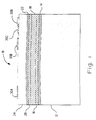
- Figure 1 is a side cross-sectional view of one preferred embodiment of a glass-coated article 10 made according to the present invention, which preferred embodiment may be used as a printed circuit board.
- Circuit board 10 comprises silicon substrate or wafer 12, which preferably is of the type suitable for use in fabricating integrated circuits and solar cells.
- the substrate 12 may be of any doping, crystal, and crystal orientation type.
- adhesion layer 14 Disposed upon substrate 12 is a first adhesion layer 14 for enhancing the bonding or wetting of subsequent layers to the silicon substrate 12.
- adhesion layer 14 is made of titanium and has a thickness of about 300-2000 Angstroms (and most preferably about 500 Angstroms), but other materials and thicknesses may be used, so long as they provide enhancement of the ability of subsequent layers to bond to the silicon substrate, and other constraints (which will be discussed in greater detail below) are satisfied.
- boron oxide, silicon dioxide or tungsten may also be used without departing from this embodiment of the present invention.
- titanium it may also be partially reacted with other materials, such as silicon oxygen, etc.
- tungsten it preferably is deposited as tungsten rich mixture of tungsten and titanium, preferably in one of the following ratios, by weight, of tungsten to titanium: 95% to 5%; 90% to 10%; or 75% to 25%.
- Interlayer diffusion barrier layer 16 is disposed upon adhesion layer 14 and serves as a diffusion barrier between conductive layer 18, and adhesion layer 14 and substrate 12. That is, the chemical composition and properties of barrier layer 16 are adapted substantially to prevent diffusion of conductive layer 18 to the layers beneath it (i.e., adhesion layer 14 and substrate 12) during formation (i.e., firing) of the article 10.
- diffusion barrier layer 16 comprises a platinum film having a thickness of about 1000 Angstroms, although other materials and thicknesses may be used, so long as they act adequately to prevent diffusion of conductive layer 18 to the layers beneath it, and other design constraints are satisfied.
- Conductive layer 18 serves as the ground plane of the board 10 and preferably is made of gold, silver, or some other highly conductive metal and has a thickness of several microns.
- the type of conductive material chosen is variable, but must be compatible with the process of the subject invention, which will be discussed in detail shortly.
- Another diffusion barrier layer 20 is disposed on top of conductive layer 18 and serves as a diffusion barrier between conductive layer 18 and the glass adhesion layer 22.
- the composition and thickness of layer 20 are substantially similar to those of barrier layer 16; however, if required by particular design considerations, layer 20 may be different from layer 16, so long as it substantially prevents diffusion between adhesion layer 22 and conductive layer 18.
- Adhesion layer 22 of titanium, boron oxide or tungsten, is disposed upon diffusion barrier layer 20 and serves to enhance the bonding or wetting of glass layer 24 to diffusion barrier layer 20.
- adhesion layer 22 is of the same composition and thickness as adhesion layer 14.
- adhesion layer 22 is used to enhance the bonding of glass layer 24 to diffusion barrier layer 20 in accordance with the process of the present invention, the uniformity of the glass layer 24 is substantially improved over the prior art and the problems associated with "roll back" of the edges of the glass layer during firing of the article substantially may be eliminated.
- glass layer 24 Disposed upon glass adhesion layer 22 is glass layer 24 which serves to electrically isolate and capacitively de-couple conventional discrete electronic components 30A..30D (mounted on or in glass layer 24) from each other, ground plane 18, and substrate 12.
- glass layer 24 is between 25 and 250 ⁇ m in thickness and is of a borosilicate glass composition.
- glass layer 24 is made of a glass such as Corning 7070 borosilicate glass which has a thermal coefficient of expansion that is substantially equal to silicon over the typical operating temperature range of the circuit board (i.e., -65°C to 400°, a maximum loss tangent of 0.06 percent and a minimum dielectric constant of 4.1 at 20 °C and 1 MHz.
- the glass layer 24 will exhibit thermal expansion characteristics that are substantially identical to those of the underlying silicon 12, and that adequately electrically and capacitively de-couples the components 30A...30D from themselves, the ground plane 18, and the substrate 12.
- other types of glass compositions may be employed for layer 24, but preferably they exhibit electrical and thermal characteristics that are substantially the same as those of Corning 7070 glass.
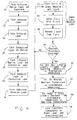
- a preferred fabrication sequence for producing the article 10 of Figure 1 is comprised of steps represented by blocks 32 through 56. It should be understood from the outset that unless otherwise specified, any conventional method may be employed to perform any of the formation and/or deposition steps discussed herein.
- the process begins by forming the first adhesion layer on the silicon substrate at block 32. After formation of the first adhesion layer, the first diffusion barrier layer is formed on the first adhesion layer at block 34. The conductive ground plane layer is then formed on the first diffusion barrier layer at block 36. Thereafter, the second diffusion barrier layer is formed on top of the conductive layer at block 38. The second adhesion layer is then formed on the second barrier layer at block 40.
- the glass material is then applied to top of the second adhesion layer.
- application of the glass material is accomplished by forming a slurry or paste of powdered ("frit") glass material in liquid at block 42.
- the liquid is a room-temperature volatile organic solvent (e.g., alcohol) and/or water.
- the slurry is composed of equal volumes of liquid and glass and is of low enough viscosity to permit spraying of the slurry onto the adhesion layer.
- the glass frit material has an average granular size of about 44 ⁇ m (325 Mesh).
- the slurry is then sprayed onto the top of the second adhesion layer at block 44.
- this is accomplished by spraying the slurry onto the second adhesion layer, permitting the slurry to dry, and repeating the spraying and drying steps, in sequence, until sufficient glass material has been deposited onto the article at block 46 to produce the desired thickness of glass layer 24 after firing.
- the liquid may be removed from the slurry in between the repeated sprayings by appropriately elevating and then maintaining the temperature to evaporate or otherwise decompose the liquid to remove it from the slurry at block 46.
- the article is fired under ambient pressure conditions to melt the glass material and to form a substantially uniform layer of glass material on the article.
- firing is conducted in stages including a first stage which comprises, over a time period of about one to two hours, preferably about one hour, linearly increasing (i.e., ramping up) the temperature of the article from the initial or beginning ambient temperature (i.e., about 20°C or higher, if the temperature has already been increased to evaporate the liquid) to an intermediate temperature of about 900 to 1025°C, preferably 1025°C at block 50.
- any remaining liquid in the slurry is driven off.
- the intermediate temperature is maintained for a period of time, e.g. 15 to 45 minutes, most preferably about 30 minutes, to melt and flow the glass particles at block 52.
- the temperature is linearly decreased (i.e., ramped down) from the intermediate temperature to the beginning or ambient temperature at block 54.
- the second adhesion material layer increases the ability of the glass to bond to the underlying article such that the problems of edge "roll-back" and other nonuniformities are substantially eliminated from the resulting glass layer.
- the process of the present invention produces a glass-coated article wherein the glass layer is substantially uniform and free of edge "roll-back” and other deformities.
- the use of the barrier layers prevent the various layers separated by them from being diffused into each other during firing of the article.
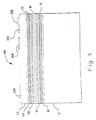
- Figure 3 is a side, cross-sectional view of another preferred embodiment 60 of the article of the present invention.
- Article 60 may be used as a printed circuit board and, with the exception of the inclusion of additional diffusion barrier layer 62 and additional adhesion layer 64, is substantially identical to embodiment 10 of Figure 1.
- diffusion barrier layer 62 is made of silicon dioxide formed by thermal oxidation of substrate 12, and helps to prevent adhesion layer 14 and diffusion barrier layer 16 from being diffused into substrate 12 during firing.
- Additional adhesion layer 64 is also preferably made of silicon dioxide, and increases the glass wetting characteristics of adhesion layer 22.
- the process used to form article 60 is identical to that used to construct article 10, except that steps 70,72 for forming layers 62 and 64, respectively, are included in the process for forming article 10.
- the preferred process for forming article 60 is illustrated in block diagram form in Figure 4.
- the materials of the adhesion, conducting, and barrier layers may be varied, so long as the aforesaid design constraints are satisfied, and the materials are compatible with the temperatures being used in the firing process.
- the materials used in the adhesion, conducting the barrier layers should have melting temperatures above the temperatures used in the firing of the article to melt the glass material.
- silicon substrate topography and/or type may be varied, for example, using a highly doped or float zone silicon.
- the environment in which the articles 10, 60 are fired may be varied. For example, rather than firing under air, firing may be conducted, for example, under an inert hydrogen atmosphere.
- an intermediate temperature of about 800°C For firing under hydrogen, an intermediate temperature of about 800°C has been found to be preferred. Of course, other temperatures, pressures, and environments may be used, assuming compliance exists with the above-presented principles of the present invention. Additionally, and depending upon the type of binder used in the slurry, the process of the present invention may include the additional step of initially ramping up the temperature of the article to a lower intermediate temperature of about 150-500°C, and holding it there for about 15-30 minutes to completely burn off the binder liquid in the slurry, before proceeding to the intermediate temperature. Additionally, the adhesion or wetting layer may be patterned prior to adding the glass such as to leave voids whereby to produce a product having a glass layer with built-in vias with access to ground.
Landscapes
- Laminated Bodies (AREA)
- Glass Compositions (AREA)
Claims (33)
- Prozeß zum Herstellen eines gebrannten glasbeschichteten Artikels (10) mit einem Siliziumsubstrat (12), mit den folgenden Schritten:dadurch gekennzeichnet, daß die Zwischenschicht, auf der die Schicht aus Glasmaterial (24) ausgebildet ist, eine Schicht aus Glashaftmaterial (22) ausgewählt aus Titan, Boroxid und Wolfram ist.(a) Ausbilden mindestens einer Zwischenschicht (14, 16, 18, 20, 22) auf dem Substrat;(b) Ausbilden einer Schicht aus Glasmaterial (24) über der Zwischenschicht oder den Zwischenschichten; und(c) Brennen des Produkts von Schritt (b), um das Glasmaterial zu schmelzen und eine im wesentlichen gleichförmige Schicht aus Glasmaterial auszubilden,
- Prozeß nach Anspruch 1, weiterhin mit dem Schritt des Ausbildens einer Schicht aus leitendem Material (18) zwischen dem Substrat (12) und dem Haftmaterial (22).
- Prozeß nach Anspruch 2, weiterhin mit dem Schritt des Ausbildens einer Diffusionssperrschicht (16) zwischen dem Substrat (12) und dem leitenden Material (18).
- Prozeß nach Anspruch 3, wobei die Diffusionssperrschicht (16) aus Platin besteht.
- Prozeß nach Anspruch 3 oder 4, wobei eine zweite Diffusionssperrschicht (20) zwischen dem leitenden Material (18) und der Glashaftschicht (22) ausgebildet wird.
- Prozeß nach einem der vorhergehenden Ansprüche, wobei der Wärmeausdehnungskoeffizient des Glasmaterials (24) über einen gewünschten Temperaturbereich hinweg im wesentlichen gleich dem des Substrats (12) ist.
- Prozeß nach einem der vorhergehenden Ansprüche, wobei das Glasmaterial Borsilikatglas umfaßt.
- Prozeß nach einem der vorhergehenden Ansprüche, wobei die Zwischenschichten zwischen dem Substrat und der mindestens einen Zwischenschicht mindestens eine zusätzliche Schicht (14) aus Haftmaterial enthält.
- Prozeß nach Anspruch 8, wobei eine Schicht (62) aus Siliziumdioxid auf dem Substrat (12) unter der zusätzlichen Schicht (14) aus Haftmaterial ausgebildet wird.
- Prozeß nach einem der vorhergehenden Ansprüche, wobei das Glasmaterial eine maximale Verlusttangente von 0,06% und eine minimale Dielektrizitätskonstante von 4,1, beide gemessen bei 20°C und 1 MHz, aufweist.
- Prozeß nach einem der vorhergehenden Ansprüche, wobei die Schicht aus Glasmaterial (24) durch die folgenden Schritte in der folgenden Reihenfolge ausgebildet wird:(i) Ausbilden einer Aufschlämmung aus Glasmaterial und einer Flüssigkeit;(ii) Aufbringen der resultierenden Aufschlämmung auf die Schicht (22) aus Haftmaterial;(iii) Entfernen der Flüssigkeit aus der Aufschlämmung; und(iv) gegebenenfalls Wiederholen der Schritte (ii)-(iii), bis man das Glasmaterials in einer gewünschten Dicke erhalten hat.
- Prozeß nach Anspruch 11, wobei die Flüssigkeit Wasser umfaßt und das Glasmaterial in Form einer Glasfritte mit einer mittleren Teilchengröße von etwa 44 um (Maschenweite 325) vorliegt.
- Prozeß nach Anspruch 11 oder 12, wobei der Schritt (iii) des Entfernens der Flüssigkeit aus der Aufschlämmung das Erhöhen der Temperatur des Artikels aus Schritt (ii) auf eine Temperatur umfaßt, die ausreicht, um die Flüssigkeit aus der Aufschlämmung zu entfernen.
- Prozeß nach Anspruch 13, wobei der Schritt (iii) die Schritte des anfänglichen Hochfahrens der Temperatur auf zwischen 150 und 500°C und des Aufrechterhaltens der Temperatur für 15 bis 30 Minuten auf diesem Wert umfaßt.
- Prozeß nach einem der vorhergehenden Ansprüche, wobei das Brennen einen mehrstufigen Prozeß umfaßt, der die folgenden Schritte in der folgenden Reihenfolge umfaßt:(i) anfängliches, im wesentlichen lineares Erhöhen der Temperatur des Artikels auf eine Zwischentemperatur im Bereich von 800 bis 1200°C;(ii) Halten des Artikels auf der Zwischentemperatur über einen Zeitraum hinweg; und(iii) im wesentlichen lineares Abkühlen des Artikels von der Zwischentemperatur auf Umgebungstemperatur.
- Prozeß nach Anspruch 15, wobei der Artikel auf eine Zwischentemperatur von etwa 1025°C erwärmt wird.
- Prozeß nach Anspruch 15 oder 16, wobei der Artikel 15 bis 45 Minuten lang auf der Zwischentemperatur gehalten wird.
- Prozeß nach Anspruch 17, wobei der Artikel etwa 30 Minuten lang auf der Zwischentemperatur gehalten wird.
- Prozeß nach einem der Ansprüche 15 bis 18, wobei der Artikel über einen Zeitraum von zwei bis fünf Stunden von der Zwischentemperatur auf Umgebungstemperatur abgekühlt wird.
- Prozeß nach Anspruch 19, wobei der Artikel über einen Zeitraum von etwa 2 Stunden abgekühlt wird.
- Prozeß nach einem der Ansprüche 15 bis 20, wobei der Artikel in ein bis zwei Stunden auf die Zwischentemperatur erwärmt wird.
- Prozeß nach einem der vorhergehenden Ansprüche, weiterhin mit dem Schritt des Ausbildens einer Schicht (64) aus Siliziumdioxid zwischen dem Glas (24) und der Glashaftschicht (22).
- Prozeß nach Anspruch 22, wobei die Schicht aus Siliziumdioxid durch thermische Aufwachstechniken ausgebildet wird.
- Artikel, der folgendes umfaßt: ein Siliziumsubstrat (12) und eine Schicht aus Glasmaterial (24) auf dem Substrat, eine Haftschicht (22) zwischen dem Substrat und der Glasmaterialschicht und mindestens ein Schaltungselement (30), das auf der Glasschicht (24) angeordnet ist,
dadurch gekennzeichnet, daß die Schicht aus Gla-shaftmaterial (22) ausgewählt ist aus Titan, Boroxid und Wolfram. - Artikel nach Anspruch 24, weiterhin mit einer leitenden Schicht (18) mit einer Diffusionssperrschicht (16, 20), die auf einer Seite davon zwischen der Glashaftschicht (22) und dem Substrat (12) angeordnet ist.
- Artikel nach Anspruch 25, wobei Diffusionssperrschichten (16, 20) auf beiden Seiten der leitenden Schicht (18) angeordnet sind.
- Artikel nach Anspruch 25 oder 26, wobei die Diffusionssperrschicht oder die Diffusionssperrschichten aus Platin bestehen.
- Artikel nach einem der Ansprüche 24 bis 27, weiterhin mit einer zwischen einer Seite der leitenden Schicht (18) und dem Substrat (12) angeordneten zweiten Haftschicht (14).
- Artikel nach einem der Ansprüche 24 bis 28, wobei das Glasmaterial eine Verlusttangente von höchstens 0,06% und eine Dielektrizitätskonstante von mindestens 4,1 aufweist.
- Artikel nach einem der Ansprüche 24 bis 29, wobei der Wärmeausdehnungskoeffizient des Glasmaterials (24) im wesentlichen gleich dem des Substrats ist.
- Artikel nach einem der Ansprüche 24 bis 30, wobei das Glasmaterial (24) Borsilikatglas umfaßt.
- Artikel nach einem der Ansprüche 24 bis 31, wobei die Schicht aus Glasmaterial (24) eine aus einer Reihe von Schichten aus Glasmaterial ausgebildete aufgebaute Schicht umfaßt.
- Artikel nach einem der Ansprüche 24 bis 32, weiterhin mit einer Schicht aus Siliziumdioxid (64) zwischen der Glashaftschicht (22) und dem Glas (24).
Applications Claiming Priority (3)
| Application Number | Priority Date | Filing Date | Title |
|---|---|---|---|
| US381735 | 1995-02-01 | ||
| US08/381,735 US5639325A (en) | 1995-02-01 | 1995-02-01 | Process for producing a glass-coated article |
| PCT/US1996/000226 WO1996024163A1 (en) | 1995-02-01 | 1996-01-03 | Process for producing a glass-coated article and article produced thereby |
Publications (2)
| Publication Number | Publication Date |
|---|---|
| EP0807318A1 EP0807318A1 (de) | 1997-11-19 |
| EP0807318B1 true EP0807318B1 (de) | 2002-04-10 |
Family
ID=23506179
Family Applications (1)
| Application Number | Title | Priority Date | Filing Date |
|---|---|---|---|
| EP96902619A Expired - Lifetime EP0807318B1 (de) | 1995-02-01 | 1996-01-03 | Herstellung eines glasüberzogenen artikels und produkt |
Country Status (4)
| Country | Link |
|---|---|
| US (1) | US5639325A (de) |
| EP (1) | EP0807318B1 (de) |
| DE (1) | DE69620587T2 (de) |
| WO (1) | WO1996024163A1 (de) |
Families Citing this family (10)
| Publication number | Priority date | Publication date | Assignee | Title |
|---|---|---|---|---|
| US5912046A (en) * | 1993-11-16 | 1999-06-15 | Form Factor, Inc. | Method and apparatus for applying a layer of flowable coating material to a surface of an electronic component |
| US6191048B1 (en) | 1997-12-31 | 2001-02-20 | The Whitaker Corporation | Process for manufacturing composite glass/Si substrates for microwave integrated circuit fabrication |
| US6379785B1 (en) | 1997-12-31 | 2002-04-30 | Tyco Electronic Corp | Glass-coated substrates for high frequency applications |
| US6582777B1 (en) * | 2000-02-17 | 2003-06-24 | Applied Materials Inc. | Electron beam modification of CVD deposited low dielectric constant materials |
| US6667549B2 (en) | 2002-05-01 | 2003-12-23 | Bridgewave Communications, Inc. | Micro circuits with a sculpted ground plane |
| JP5027992B2 (ja) * | 2002-05-23 | 2012-09-19 | ショット アクチエンゲゼルシャフト | 高周波用途のためのガラス材料 |
| US6764927B1 (en) * | 2003-04-24 | 2004-07-20 | Taiwan Semiconductor Manufacturing Co., Ltd | Chemical vapor deposition (CVD) method employing wetting pre-treatment |
| DE102006046961A1 (de) * | 2006-10-04 | 2008-04-10 | Leibniz-Institut Für Neue Materialien Gemeinnützige Gmbh | Herstellung einer flexiblen, gasdichten und transparenten Verbundfolie |
| US8707734B2 (en) * | 2009-10-19 | 2014-04-29 | The Regents Of The University Of Michigan | Method of embedding material in a glass substrate |
| DE102018112069A1 (de) * | 2018-05-18 | 2019-11-21 | Schott Ag | Verwendung eines Flachglases in elektronischen Bauteilen |
Family Cites Families (24)
| Publication number | Priority date | Publication date | Assignee | Title |
|---|---|---|---|---|
| US3247428A (en) * | 1961-09-29 | 1966-04-19 | Ibm | Coated objects and methods of providing the protective coverings therefor |
| US3303399A (en) * | 1964-01-30 | 1967-02-07 | Ibm | Glasses for encapsulating semiconductor devices and resultant devices |
| US3212921A (en) * | 1961-09-29 | 1965-10-19 | Ibm | Method of forming a glass film on an object and the product produced thereby |
| US3361592A (en) * | 1964-03-16 | 1968-01-02 | Hughes Aircraft Co | Semiconductor device manufacture |
| USB534135I5 (de) * | 1966-03-14 | |||
| US3496631A (en) * | 1967-02-08 | 1970-02-24 | Gordon Kowa Cheng Chen | Manufacture of semi-conductor devices |
| US3632433A (en) * | 1967-03-29 | 1972-01-04 | Hitachi Ltd | Method for producing a semiconductor device |
| GB1255995A (en) * | 1968-03-04 | 1971-12-08 | Hitachi Ltd | Semiconductor device and method of making same |
| US3632434A (en) * | 1969-01-21 | 1972-01-04 | Jerald L Hutson | Process for glass passivating silicon semiconductor junctions |
| US3760242A (en) * | 1972-03-06 | 1973-09-18 | Ibm | Coated semiconductor structures and methods of forming protective coverings on such structures |
| DE2517743C3 (de) * | 1975-04-22 | 1980-03-06 | Jenaer Glaswerk Schott & Gen., 6500 Mainz | Passivierender Schutzüberzug für Siliziumhalbleiterbauelemente |
| US4093771A (en) * | 1976-10-29 | 1978-06-06 | Nasa | Reaction cured glass and glass coatings |
| US4369254A (en) * | 1980-10-17 | 1983-01-18 | Rca Corporation | Crossover dielectric inks |
| US4344985A (en) * | 1981-03-27 | 1982-08-17 | Rca Corporation | Method of passivating a semiconductor device with a multi-layer passivant system by thermally growing a layer of oxide on an oxygen doped polycrystalline silicon layer |
| JPS58186948A (ja) * | 1982-04-26 | 1983-11-01 | Nippon Telegr & Teleph Corp <Ntt> | 誘電体分離した半導体基板の製造方法 |
| JPH0618234B2 (ja) * | 1985-04-19 | 1994-03-09 | 日本電信電話株式会社 | 半導体基板の接合方法 |
| DE3516222A1 (de) * | 1985-05-06 | 1986-11-06 | Siemens AG, 1000 Berlin und 8000 München | Halbleiterbauelement mit erhoehter oberflaechen-durchbruchsspannung |
| JPS62122152A (ja) * | 1985-11-21 | 1987-06-03 | Sumitomo Electric Ind Ltd | 半導体装置用基板の製造方法 |
| US4764486A (en) * | 1986-01-23 | 1988-08-16 | Matsushita Electric Works, Ltd. | Sintered glass-powder product |
| US4737236A (en) * | 1986-09-08 | 1988-04-12 | M/A-Com, Inc. | Method of making microwave integrated circuits |
| US4781775A (en) * | 1987-06-01 | 1988-11-01 | Motorola Inc. | Coplanar die to substrate bond method |
| US4788163A (en) * | 1987-08-20 | 1988-11-29 | General Electric Company | Devitrifying glass frits |
| US5212121A (en) * | 1990-06-13 | 1993-05-18 | Mitsui Mining Company, Limited | Raw batches for ceramic substrates, substrates produced from the raw batches, and production process of the substrates |
| JPH052117A (ja) * | 1991-06-25 | 1993-01-08 | Fujikura Ltd | シリコン基板上に光導波路用石英薄膜を形成する方法 |
-
1995
- 1995-02-01 US US08/381,735 patent/US5639325A/en not_active Expired - Lifetime
-
1996
- 1996-01-03 WO PCT/US1996/000226 patent/WO1996024163A1/en not_active Ceased
- 1996-01-03 EP EP96902619A patent/EP0807318B1/de not_active Expired - Lifetime
- 1996-01-03 DE DE69620587T patent/DE69620587T2/de not_active Expired - Lifetime
Also Published As
| Publication number | Publication date |
|---|---|
| WO1996024163A1 (en) | 1996-08-08 |
| US5639325A (en) | 1997-06-17 |
| DE69620587D1 (de) | 2002-05-16 |
| DE69620587T2 (de) | 2002-10-31 |
| EP0807318A1 (de) | 1997-11-19 |
Similar Documents
| Publication | Publication Date | Title |
|---|---|---|
| US5277725A (en) | Process for fabricating a low dielectric composite substrate | |
| US4340436A (en) | Process for flattening glass-ceramic substrates | |
| US7135767B2 (en) | Integrated circuit substrate material and method | |
| US4409278A (en) | Blister-free direct bonding of metals to ceramics and metals | |
| US5283104A (en) | Via paste compositions and use thereof to form conductive vias in circuitized ceramic substrates | |
| CA2211533C (en) | Glass bonding layer for a ceramic circuit board support substrate | |
| EP0807318B1 (de) | Herstellung eines glasüberzogenen artikels und produkt | |
| DE69122958T2 (de) | Direktes verbinden von kupfer auf aluminiumnitridsubstrate | |
| GB2274353A (en) | Connections for semiconductor devices | |
| US4781970A (en) | Strengthening a ceramic by post sinter coating with a compressive surface layer | |
| EP0798781B1 (de) | Siliziumnitrid-Platine und ihre Herstellung | |
| US5070393A (en) | Aluminum nitride substrate for formation of thin-film conductor layer and semiconductor device using the substrate | |
| CA2057490C (en) | Laminated diamond substrate | |
| US5139851A (en) | Low dielectric composite substrate | |
| US6379785B1 (en) | Glass-coated substrates for high frequency applications | |
| Brown | RF/microwave hybrids: basics, materials and processes | |
| EP0113088B1 (de) | Trägersubstrat für Halbleiterelement | |
| JPH118239A (ja) | 半導体装置の製造方法 | |
| JPH0447978B2 (de) | ||
| US6191048B1 (en) | Process for manufacturing composite glass/Si substrates for microwave integrated circuit fabrication | |
| WO1997013274A1 (en) | A support for electronic components | |
| JPS63136410A (ja) | 厚膜銅ビア充填インキ | |
| JPH02116196A (ja) | セラミック多層回路基板の製造方法 | |
| US5554884A (en) | Multilevel metallization process for use in fabricating microelectronic devices | |
| JP3241537B2 (ja) | ガラスセラミック基板 |
Legal Events
| Date | Code | Title | Description |
|---|---|---|---|
| PUAI | Public reference made under article 153(3) epc to a published international application that has entered the european phase |
Free format text: ORIGINAL CODE: 0009012 |
|
| 17P | Request for examination filed |
Effective date: 19970829 |
|
| AK | Designated contracting states |
Kind code of ref document: A1 Designated state(s): DE FR GB |
|
| 17Q | First examination report despatched |
Effective date: 19981228 |
|
| GRAG | Despatch of communication of intention to grant |
Free format text: ORIGINAL CODE: EPIDOS AGRA |
|
| GRAG | Despatch of communication of intention to grant |
Free format text: ORIGINAL CODE: EPIDOS AGRA |
|
| GRAH | Despatch of communication of intention to grant a patent |
Free format text: ORIGINAL CODE: EPIDOS IGRA |
|
| REG | Reference to a national code |
Ref country code: GB Ref legal event code: IF02 |
|
| GRAH | Despatch of communication of intention to grant a patent |
Free format text: ORIGINAL CODE: EPIDOS IGRA |
|
| GRAA | (expected) grant |
Free format text: ORIGINAL CODE: 0009210 |
|
| RBV | Designated contracting states (corrected) |
Designated state(s): DE FR GB |
|
| AK | Designated contracting states |
Kind code of ref document: B1 Designated state(s): DE FR GB |
|
| REF | Corresponds to: |
Ref document number: 69620587 Country of ref document: DE Date of ref document: 20020516 |
|
| ET | Fr: translation filed | ||
| PLBE | No opposition filed within time limit |
Free format text: ORIGINAL CODE: 0009261 |
|
| STAA | Information on the status of an ep patent application or granted ep patent |
Free format text: STATUS: NO OPPOSITION FILED WITHIN TIME LIMIT |
|
| 26N | No opposition filed |
Effective date: 20030113 |
|
| REG | Reference to a national code |
Ref country code: GB Ref legal event code: 732E Free format text: REGISTERED BETWEEN 20090319 AND 20090325 |
|
| REG | Reference to a national code |
Ref country code: FR Ref legal event code: TP |
|
| REG | Reference to a national code |
Ref country code: GB Ref legal event code: 732E Free format text: REGISTERED BETWEEN 20100114 AND 20100120 |
|
| PGFP | Annual fee paid to national office [announced via postgrant information from national office to epo] |
Ref country code: GB Payment date: 20091223 Year of fee payment: 15 |
|
| PGFP | Annual fee paid to national office [announced via postgrant information from national office to epo] |
Ref country code: FR Payment date: 20100209 Year of fee payment: 15 |
|
| PGFP | Annual fee paid to national office [announced via postgrant information from national office to epo] |
Ref country code: DE Payment date: 20100326 Year of fee payment: 15 |
|
| REG | Reference to a national code |
Ref country code: FR Ref legal event code: TP |
|
| GBPC | Gb: european patent ceased through non-payment of renewal fee |
Effective date: 20110103 |
|
| REG | Reference to a national code |
Ref country code: FR Ref legal event code: ST Effective date: 20110930 |
|
| PG25 | Lapsed in a contracting state [announced via postgrant information from national office to epo] |
Ref country code: FR Free format text: LAPSE BECAUSE OF NON-PAYMENT OF DUE FEES Effective date: 20110131 |
|
| PG25 | Lapsed in a contracting state [announced via postgrant information from national office to epo] |
Ref country code: GB Free format text: LAPSE BECAUSE OF NON-PAYMENT OF DUE FEES Effective date: 20110103 |
|
| REG | Reference to a national code |
Ref country code: DE Ref legal event code: R119 Ref document number: 69620587 Country of ref document: DE Effective date: 20110802 |
|
| PG25 | Lapsed in a contracting state [announced via postgrant information from national office to epo] |
Ref country code: DE Free format text: LAPSE BECAUSE OF NON-PAYMENT OF DUE FEES Effective date: 20110802 |