EP0806080B1 - Amplificateur - Google Patents
Amplificateur Download PDFInfo
- Publication number
- EP0806080B1 EP0806080B1 EP95921001A EP95921001A EP0806080B1 EP 0806080 B1 EP0806080 B1 EP 0806080B1 EP 95921001 A EP95921001 A EP 95921001A EP 95921001 A EP95921001 A EP 95921001A EP 0806080 B1 EP0806080 B1 EP 0806080B1
- Authority
- EP
- European Patent Office
- Prior art keywords
- current
- voltage
- amplifier
- transistor
- input
- Prior art date
- Legal status (The legal status is an assumption and is not a legal conclusion. Google has not performed a legal analysis and makes no representation as to the accuracy of the status listed.)
- Expired - Lifetime
Links
Images

Classifications
-
- H—ELECTRICITY
- H03—ELECTRONIC CIRCUITRY
- H03F—AMPLIFIERS
- H03F3/00—Amplifiers with only discharge tubes or only semiconductor devices as amplifying elements
- H03F3/45—Differential amplifiers
- H03F3/45071—Differential amplifiers with semiconductor devices only
- H03F3/45479—Differential amplifiers with semiconductor devices only characterised by the way of common mode signal rejection
Definitions
- the relative dimensions of the transistor current mirrors establish the current ratios existing in the network of transistor current mirrors.
- the network of transistor current mirrors includes a first transistor current mirror, a second transistor current mirror and a third transistor current mirror, the third transistor current mirror being connected to receive current from the first transistor current mirror, the second and third transistor current mirrors, in operation, providing the first and second currents.
- a capacitor is connected to a port of the voltage-cancellation circuit and determines the bandwidth of the voltage-cancellation circuit.
- one transistor of the differentially-connected input stage is provided with a fixed base voltage bias and the base voltage bias of the opposing transistor of the differentially-connected input stage is provided by the voltage cancellation circuit.
- the differentially-connected input stage includes current-feedback circuits for increasing the base input impedances of the transistors.
- the current amplifier includes the second resistor connectible by switch elements between the second output stage and the further low impedance input port of the current-summing stage when the second output stage is in operation, the values of the resistors being such as to maintain the same transresistance of the current amplifier when the second output stage is in operation.
- the reference and output stages include respective pairs of field-effect transistors, connected in push-pull, so coupled to the voltage-amplifying stage as to be biassed in class AB.
- the voltage-amplifying stage includes an input voltage buffer connected to drive current into a network of field-effect transistors including the further complementary pair of field-effect transistors.
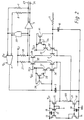
- the source electrodes of the transistors 13,15,17 are connected together and to a first terminal of a voltage source, the gate electrodes of the transistors 13,15,17 are connected together and to the drain electrode of the transistor 17. Further, the source electrodes of the transistors 14,16 are connected together and through a nominal parasitic series impedance represented by a resistor 101 to a second terminal (of voltage lower than that provided at the first terminal) of the voltage source, the gate electrodes of the transistors 14,16 are connected together and to the drain electrode of the transistor 14.
- the collector electrode of the transistor 2 is connected to a second input terminal of the intermediate amplifying circuit 4 a second output terminal of which is connected to a second input terminal of the output voltage amplifying circuit 5, a second output terminal of the output voltage amplifying circuit 5 providing a second output terminal 24 of the amplifier.
- the base electrode of the transistor 2 is connected to one terminal of a capacitor 10 the other terminal of which is connected to the source electrodes of the transistors 14,16.
- a resistor 11 is connected between the base electrode of the transistor 2 and the base electrode of an NPN bipolar transistor 12 which has its emitter electrode connected to a voltage reference source, there being a current source in the collector circuit of the transistor 12 which has a connection between its collector and base electrodes.
- V M is the nominal common-mode output voltage of the output voltage amplifying circuit 5.
- the voltage V M is applied to another input terminal of the voltage cancellation circuit 6 and a voltage V Q is applied to yet another input terminal of the voltage cancellation circuit 6.
- the voltage V Q is the estimated voltage for the base electrode of the transistor 1.
- Fig. 1 shows a resistive element 100 connected between the input terminals 1,2 of the amplifier.
- the resistive element 100 represents a magnetoresistive element that may be included in the reading head of a magnetic-disc drive used in a computer, say.
- the resistance of the magnetoresistive element varies in accordance with the magnetic signature of a disc over which a reading head containing the magnetoresistive element 100 is being guided.
- Current injected by the current generator connected to the input terminals 20,21 gives rise to a d.c. voltage across the magnetoresistive element 100.
- the magnetically-induced variation of the resistance of the magnetoresistive element 100 gives rise to an a.c. modulation of the voltage across the terminals 20,21 of the amplifier.
- the magnetoresistive element 100 is not a part of the amplifier.
- the current generator included in Fig. 1 serves to provide a bias current for the resistive element 100 and equal bias currents for the transistors 1,2.
- a control current I BR is drawn from the drain electrode of the transistor 17 and an effect of the arrangement of the transistor 15 relative to the transistor 17 is to make a current of 32 I BR - I E available from the drain electrode of the transistor 15 to the terminal 20, I E being the emitter bias current of each of the transistors 1,2.
- An effect of the arrangement of the transistors 13,14,16 relative to the transistor 17 is to make the transistor 16 capable of drawing a current of 32 I BR + I E at its drain electrode.
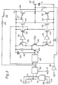
- An additional class-AB output stage is present in the form of the transistors 308,315 the gate electrodes of which are connectible by way of switch elements 311,317 to the output terminals of the unity-gain voltage amplifiers 310,316 for providing enhanced current drive to the output terminal 321.
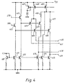
- a further input differential current could be applied to the common emitter electrodes of the transistors 515,516 and 523,524 through additional input terminals in a similar way to that in which input currents are applied to the transistors 503,506 and 505,508 through the input terminals 540,541.
- the quiescent voltage of the additional input terminals would be VQ rather than VM.
Landscapes
- Engineering & Computer Science (AREA)
- Power Engineering (AREA)
- Amplifiers (AREA)
- Recording Or Reproducing By Magnetic Means (AREA)
Claims (25)
- Amplificateur incluant :caractérisé en ce que le générateur de courant (13 à 19) inclut un réseau de miroirs de courant à transistors (13 à 17) qui, en fonctionnement, délivrent un premier courant à une première borne (20) et tirent un second courant à une seconde borne (21) du point d'accès d'entrée (20, 21), les premier et second courants étant inégaux.un générateur de courant (13 à 19), connecté à un de ses points d'accès d'entrée (20, 21) pour, en fonctionnement, injecter un courant dans une charge qui, en fonctionnement, est connectée audit point d'accès (20, 21) de l'amplificateur,un circuit d'amplification accordé en fréquence (1 à 4,10) connecté audit point d'accès d'entrée (20, 21), le circuit d'amplification accordé en fréquence (1 à 4,10), en fonctionnement, amplifiant les signaux d'entrée excluant le courant injecté présent au niveau dudit point d'accès d'entrée (20, 21) etun circuit d'annulation de tension (6) connecté à l'intérieur du circuit d'amplification accordé en fréquence (1 à 4,10), le circuit d'annulation de tension (6), en fonctionnement, opposant une condition de déséquilibre à l'intérieur du circuit d'amplification accordé en fréquence (1 à 4,10) attribuable au courant injecté,
- Amplificateur selon la revendication 1 dans lequel les dimensions relatives des miroirs de courant à transistors (13 à 17) établissent les rapports de courant existant dans le réseau de miroirs de courant à transistors (13 à 17).
- Amplificateur selon la revendication 2, dans lequel le réseau de miroirs de courant à transistors (13 à 17) inclut un premier miroir de courant à transistors (13, 17), un second miroir de courant à transistors (15, 17) et un troisième miroir de courant à transistors (14, 16), le troisième miroir de courant à transistors (14, 16) étant connecté pour recevoir le courant provenant du premier miroir de courant à transistors (13, 17), les second et troisième miroirs de courant à transistors (15, 17 ; 14, 16) en fonctionnement, délivrant les premier et second courants.
- Amplificateur selon l'une quelconque des revendications 1 à 3, dans lequel le circuit d'annulation de tension (6) est connecté pour répondre, en fonctionnement, à une tension de sortie à courant continu provenant du circuit d'amplification accordé en fréquence (1 à 4,10) et pour appliquer un signal à un élément d'entrée du circuit d'amplification accordé en fréquence (1 à 4,10) dans un sens tel à amener la tension de sortie à courant continu du circuit d'amplification accordé en fréquence (1 à 4,10) vers une tension de zéro volt.
- Amplificateur selon l'une quelconque des revendications 1 à 4, dans lequel le circuit d'annulation de tension (6) fonctionne initialement avec une première largeur de bande et un premier gain et, ultérieurement, avec une seconde largeur de bande qui est plus étroite que la première largeur de bande et avec un second gain qui est sensiblement égal au premier gain.
- Amplificateur selon l'une quelconque des revendications 1 à 5, dans lequel le circuit d'annulation de tension (6), en fonctionnement, répond à une première tension de fonctionnement à un bas niveau et à une seconde tension de fonctionnement à un niveau haut dans le circuit d'amplification accordé en fréquence (1 à 4,10) et applique un signal à un élément d'entrée du circuit d'amplification accordé en fréquence dans un sens tel à s'opposer à une déviation des première et seconde tensions de fonctionnement par rapport à des valeurs sélectionnées.
- Amplificateur selon l'une quelconque des revendications 1 à 6, dans lequel le circuit d'annulation de tension (6) inclut un étage de sortie d'amplificateur de courant qui, en fonctionnement, maintient une tension d'entrée à courant continu au niveau d'un élément d'entrée du circuit d'amplification accordé en fréquence (1 à 4,10) pour s'opposer à l'effet du courant injecté.
- Amplificateur selon l'une quelconque des revendications 1 à 6, dans lequel le circuit d'annulation de tension (6) inclut un étage de sortie d'amplificateur de tension connecté en série avec une résistance d'établissement de courant pour maintenir une tension d'entrée à courant continu au niveau d'un élément d'entrée du circuit d'amplification accordé en fréquence (1 à 4,10), pour, en fonctionnement, s'opposer à l'effet du courant injecté.
- Amplificateur selon l'une quelconque des revendications 1 à 8, dans lequel un condensateur (3) est connecté à un point d'accès du circuit d'annulation de tension (6) et détermine la largeur de bande du circuit d'annulation de tension (6).
- Amplificateur selon l'une quelconque des revendications 1 à 9, dans lequel le circuit d'amplification accordé en fréquence (1 à 4,10) inclut un étage d'entrée à transistors bipolaires connecté en différentiel connecté de façon à fonctionner en une configuration à base commune sur la plage de fréquence du circuit d'amplification accordé en fréquence (1 à4,10).
- Amplificateur selon la revendication 10, dans lequel un transistor de l'étage d'entrée connecté en différentiel reçoit une polarisation de tension de base fixe et la polarisation de tension de base du transistor opposé de l'étage d'entrée connecté en différentiel est délivrée par le circuit d'annulation de tension (6).
- Amplificateur selon la revendication 10 ou 11, dans lequel l'étage d'entrée connecté en différentiel inclut des circuits de contre-réaction de courant pour accroítre les impédances d'entrée de base des transistors.
- Amplificateur selon la revendication 10 ou 11, dans lequel chaque partie de l'étage d'entrée connecté en différentiel inclut un transistor d'entrée connecté en Darlington.
- Amplificateur selon l'une quelconque des revendications 1 à 13, dans lequel le circuit d'annulation de tension (6) inclut un amplificateur de courant comprenant :un étage de sommation de courant d'entrée (301, 302) ayant un premier point d'accès à basse impédance,un étage d'amplification de tension (303, 304, 322, 305, 309, 312) incluant un point d'accès d'entrée connecté à un point d'accès de sortie de l'étage de sommation de courant (301, 302),un étage de référence (306, 313) incluant un point d'accès de sortie qui est connecté à un second point d'accès d'entrée à basse impédance de l'étage de sommation de courant (301, 302) etun étage de sortie (307, 308, 314, 315) qui est connecté pour être attaqué par l'étage d'amplification de tension (303, 304, 322, 305, 309, 312), l'étage de sortie (307, 308, 314, 315) étant connecté en parallèle avec l'étage de référence (306, 313), les courants de sortie des étages de sortie et de référence étant à un rapport fixé l'un par rapport à l'autre comme déterminé par les éléments de l'étage de sortie (307, 308, 314, 315) et de l'étage de référence (306, 313).
- Amplificateur selon la revendication 14, dans lequel une première résistance (31) connectée depuis un point d'accès de sortie de l'étage d'amplification de tension (303, 304, 322, 305, 309, 312) jusqu'à un point de référence définit la transrésistance de l'amplificateur de courant.
- Amplificateur selon la revendication 14 ou 15, dans lequel une seconde résistance (318) connectée depuis un point d'accès de sortie de l'étage d'amplification de tension (303, 304, 322, 305, 309, 312) à un autre point d'accès d'entrée à basse impédance de l'étage de sommation de courant (301, 302) définit la transrésistance de l'amplificateur de courant.
- Amplificateur selon l'une quelconque des revendications 14 à 16, incluant un premier étage de sortie (307, 314) qui a un premier gain en courant et un second étage de sortie (308, 315) avec des points d'accès d'entrée et de sortie pouvant être connectés en parallèle aux points d'accès d'entrée et de sortie respectifs du premier étage de sortie (307, 314) au moyen d'éléments de commutation (311, 317), le second étage de sortie (308, 315) ayant un gain en courant dépassant celui du premier étage de sortie (307, 314).
- Amplificateur selon la revendication 17 lorsque dépendante de la revendication 16, dans lequel ladite seconde résistance (318) peut être connectée par un autre élément de commutation (320) entre le second étage de sortie (308, 315) et un autre point d'accès d'entrée à basse impédance de l'étage de sommation de courant (301, 302) lorsque le second étage de sortie (308, 315) est en fonctionnement, la valeur de l'autre résistance (318) étant telle à maintenir la même transrésistance de l'amplificateur de courant lorsque le second étage de sortie (308, 315) est en fonctionnement comme dans d'autres configurations.
- Amplificateur selon l'une quelconque des revendications 14 à 18, dans lequel les étages de référence et de sortie incluent des paires respectives complémentaires de transistors à effet de champ, connectés en symétrique, ainsi couplés à l'étage d'amplification de tension (303, 304, 322, 305, 309, 312) de façon à assurer le fonctionnement en classe d'amplification AB.
- Amplificateur selon la revendication 19, dans lequel l'étage d'amplification de tension (303, 304, 322, 305, 309, 312) inclut une autre paire complémentaire de transistors à effet de champ (305, 312), avec des bornes de grille connectées aux bornes de grille respectives des transistors dans les étages de référence et de sortie et des bornes de source connectées aux bornes de source respectives des transistors dans les étages de référence et de sortie.
- Amplificateur selon la revendication 20, dans lequel l'étage d'amplification de tension (303, 304, 322, 305, 309, 312) inclut un séparateur de tension d'entrée (303, 322) connecté pour amener le courant dans un réseau de transistors à effet de champ (305, 309, 312) incluant l'autre paire complémentaire de transistors à effet de champ.
- Amplificateur selon la revendication 21, dans lequel le séparateur de tension d'entrée (303, 322) inclut un transistor bipolaire d'entrée (303) connecté comme émetteur-suiveur pour entraíner le courant dans le réseau des transistors à effet de champ.
- Amplificateur selon la revendication 21, dans lequel le séparateur de tension d'entrée inclut un transistor d'entrée à effet de champ connecté comme source-suiveur pour entraíner le courant dans le réseau des transistors à effet de champ.
- Amplificateur selon l'une quelconque des revendications 17 à 23, incluant une paire complémentaire supplémentaire de transistors de sortie à effet de champ avec des bornes de grille pouvant être connectées aux bornes de grille respectives des transistors à effet de champ inclus dans l'étage de référence et des bornes de source connectées aux bornes de source respectives des transistors à effet de champ inclus dans l'étage de référence, pour délivrer un courant de sortie dépassant celui disponible à partir du premier étage de sortie.
- Amplificateur selon l'une quelconque des revendications 19 à 23, dans lequel les transistors à effet de champ sont des dispositifs en mode enrichissement.
Priority Applications (1)
| Application Number | Priority Date | Filing Date | Title |
|---|---|---|---|
| EP99203715A EP0982853A3 (fr) | 1995-01-27 | 1995-05-30 | Amplificateur |
Applications Claiming Priority (3)
| Application Number | Priority Date | Filing Date | Title |
|---|---|---|---|
| GB9501624A GB2297447A (en) | 1995-01-27 | 1995-01-27 | Amplifier |
| GB9501624 | 1995-01-27 | ||
| PCT/GB1995/001245 WO1996023352A1 (fr) | 1995-01-27 | 1995-05-30 | Amplificateur |
Related Child Applications (1)
| Application Number | Title | Priority Date | Filing Date |
|---|---|---|---|
| EP99203715A Division EP0982853A3 (fr) | 1995-01-27 | 1995-05-30 | Amplificateur |
Publications (2)
| Publication Number | Publication Date |
|---|---|
| EP0806080A1 EP0806080A1 (fr) | 1997-11-12 |
| EP0806080B1 true EP0806080B1 (fr) | 2000-06-28 |
Family
ID=10768685
Family Applications (2)
| Application Number | Title | Priority Date | Filing Date |
|---|---|---|---|
| EP95921001A Expired - Lifetime EP0806080B1 (fr) | 1995-01-27 | 1995-05-30 | Amplificateur |
| EP99203715A Withdrawn EP0982853A3 (fr) | 1995-01-27 | 1995-05-30 | Amplificateur |
Family Applications After (1)
| Application Number | Title | Priority Date | Filing Date |
|---|---|---|---|
| EP99203715A Withdrawn EP0982853A3 (fr) | 1995-01-27 | 1995-05-30 | Amplificateur |
Country Status (7)
| Country | Link |
|---|---|
| US (1) | US5923216A (fr) |
| EP (2) | EP0806080B1 (fr) |
| JP (1) | JPH10513316A (fr) |
| KR (1) | KR987001154A (fr) |
| DE (1) | DE69517706T2 (fr) |
| GB (1) | GB2297447A (fr) |
| WO (1) | WO1996023352A1 (fr) |
Cited By (1)
| Publication number | Priority date | Publication date | Assignee | Title |
|---|---|---|---|---|
| US7183850B2 (en) | 2001-09-06 | 2007-02-27 | Infineon Technologies, Ag | Switchable operational amplifier circuit |
Families Citing this family (12)
| Publication number | Priority date | Publication date | Assignee | Title |
|---|---|---|---|---|
| US6111711A (en) * | 1998-08-24 | 2000-08-29 | International Business Machines Corp. | Fast charge and thermal asperity compensation circuit |
| US6473253B1 (en) * | 1999-04-28 | 2002-10-29 | Koninklijke Philips Electronics N.V. | Read channel with programmable bandwidth control |
| US6985229B2 (en) * | 2002-05-30 | 2006-01-10 | Agere Systems, Inc. | Overlay metrology using scatterometry profiling |
| KR100433362B1 (ko) * | 2002-07-11 | 2004-06-07 | 에이디반도체(주) | 임피던스 비교 집적회로 |
| US7202744B1 (en) * | 2005-06-15 | 2007-04-10 | National Semiconductor Corporation | Transresistance amplifier |
| US7667914B2 (en) * | 2006-04-17 | 2010-02-23 | Hitachi Global Storage Technologies Netherlands B.V. | Direct coupled wide-bandwidth front-end with smart bias control amplifier |
| US7948309B2 (en) * | 2009-01-16 | 2011-05-24 | University Of Macau | DC-offset cancelled programmable gain array for low-voltage wireless LAN system and method using the same |
| RU2467471C1 (ru) * | 2011-10-18 | 2012-11-20 | Федеральное государственное бюджетное образовательное учреждение высшего профессионального образования "Южно-Российский государственный университет экономики и сервиса" (ФГБОУ ВПО "ЮРГУЭС") | Избирательный усилитель |
| RU2467469C1 (ru) * | 2011-11-21 | 2012-11-20 | Федеральное государственное бюджетное образовательное учреждение высшего профессионального образования "Южно-Российский государственный университет экономики и сервиса" (ФГБОУ ВПО "ЮРГУЭС") | Избирательный усилитель |
| RU2479109C1 (ru) * | 2012-04-12 | 2013-04-10 | Федеральное государственное бюджетное образовательное учреждение высшего профессионального образования "Южно-Российский государственный университет экономики и сервиса" (ФГБОУ ВПО "ЮРГУЭС") | Избирательный усилитель |
| RU2479110C1 (ru) * | 2012-04-16 | 2013-04-10 | Федеральное государственное бюджетное образовательное учреждение высшего профессионального образования "Южно-Российский государственный университет экономики и сервиса" (ФГБОУ ВПО "ЮРГУЭС") | Избирательный усилитель |
| US9899973B2 (en) * | 2016-03-18 | 2018-02-20 | Inphi Corporation | Split cascode circuits and related communication receiver architectures |
Family Cites Families (13)
| Publication number | Priority date | Publication date | Assignee | Title |
|---|---|---|---|---|
| US4177432A (en) * | 1978-06-26 | 1979-12-04 | National Semiconductor Corporation | Multi output differential amplifier |
| US4379267A (en) * | 1980-06-25 | 1983-04-05 | Mostek Corporation | Low power differential amplifier |
| JPS5753112A (en) * | 1980-09-16 | 1982-03-30 | Toshiba Corp | Sepp power amplifier |
| JPS592410A (ja) * | 1982-06-28 | 1984-01-09 | Sony Corp | 電流増幅器 |
| US4570128A (en) * | 1984-07-05 | 1986-02-11 | National Semiconductor Corporation | Class AB output circuit with large swing |
| JPH0720040B2 (ja) * | 1986-11-21 | 1995-03-06 | ソニー株式会社 | 電圧−電流変換回路 |
| US4843342A (en) * | 1987-12-09 | 1989-06-27 | Vtc Incorporated | Differential amplifier with input bias current cancellation |
| US5103353A (en) * | 1990-05-01 | 1992-04-07 | International Business Machines Corporation | Low noise amplifier with short circuit protection for signals from magnetoresistive element |
| US5122915A (en) * | 1990-09-26 | 1992-06-16 | Minnesota Mining And Manufacturing Company | Low-noise preamplifier for magneto-resistive heads |
| US5204789A (en) * | 1991-01-31 | 1993-04-20 | International Business Machines Corporation | Low noise voltage-biasing amplifier for magnetoresistive element |
| IT1250824B (it) * | 1991-07-29 | 1995-04-21 | Sgs Thomson Microelectrincs S | Amplificatore integrato per strumentazione con ingresso differenziale ed una singola sorgente di alimentazione, con capacita' integrate di stabilizzazione in frequenza. |
| US5293136A (en) * | 1992-09-17 | 1994-03-08 | Sgs-Thomson Microelectronics, Inc. | Two-stage rail-to-rail operational amplifier |
| US5351012A (en) * | 1993-04-02 | 1994-09-27 | Elantec, Inc. | Low input resistance current-mode feedback operational amplifier input stage |
-
1995
- 1995-01-27 GB GB9501624A patent/GB2297447A/en not_active Withdrawn
- 1995-05-30 EP EP95921001A patent/EP0806080B1/fr not_active Expired - Lifetime
- 1995-05-30 DE DE69517706T patent/DE69517706T2/de not_active Expired - Fee Related
- 1995-05-30 KR KR1019970704479A patent/KR987001154A/ko not_active Ceased
- 1995-05-30 US US08/875,568 patent/US5923216A/en not_active Expired - Fee Related
- 1995-05-30 EP EP99203715A patent/EP0982853A3/fr not_active Withdrawn
- 1995-05-30 WO PCT/GB1995/001245 patent/WO1996023352A1/fr not_active Ceased
- 1995-05-30 JP JP8522694A patent/JPH10513316A/ja active Pending
Cited By (1)
| Publication number | Priority date | Publication date | Assignee | Title |
|---|---|---|---|---|
| US7183850B2 (en) | 2001-09-06 | 2007-02-27 | Infineon Technologies, Ag | Switchable operational amplifier circuit |
Also Published As
| Publication number | Publication date |
|---|---|
| WO1996023352A1 (fr) | 1996-08-01 |
| EP0982853A2 (fr) | 2000-03-01 |
| EP0806080A1 (fr) | 1997-11-12 |
| KR987001154A (ko) | 1998-04-30 |
| EP0982853A3 (fr) | 2000-03-29 |
| GB2297447A (en) | 1996-07-31 |
| DE69517706D1 (de) | 2000-08-03 |
| JPH10513316A (ja) | 1998-12-15 |
| DE69517706T2 (de) | 2000-10-19 |
| US5923216A (en) | 1999-07-13 |
| GB9501624D0 (en) | 1995-03-15 |
Similar Documents
| Publication | Publication Date | Title |
|---|---|---|
| US5343164A (en) | Operational amplifier circuit with slew rate enhancement | |
| US4532479A (en) | Differential amplifier circuit with rail-to-rail capability | |
| US5311145A (en) | Combination driver-summing circuit for rail-to-rail differential amplifier | |
| US4586000A (en) | Transformerless current balanced amplifier | |
| US5475343A (en) | Class AB complementary output stage | |
| EP0806080B1 (fr) | Amplificateur | |
| US4783602A (en) | Operational transconductance amplifier for use in sample-and-hold circuits and the like | |
| US4901031A (en) | Common-base, source-driven differential amplifier | |
| US5351012A (en) | Low input resistance current-mode feedback operational amplifier input stage | |
| US4596958A (en) | Differential common base amplifier with feed forward circuit | |
| US5939944A (en) | NPN push-pull output stage with folded cascode JFETs | |
| US5166636A (en) | Dynamic biasing for class a amplifier | |
| US4004245A (en) | Wide common mode range differential amplifier | |
| US4801893A (en) | Forward transimpedance amplifier | |
| US6249153B1 (en) | High slew rate input differential pair with common mode input to ground | |
| US5382919A (en) | Wideband constant impedance amplifiers | |
| US4241314A (en) | Transistor amplifier circuits | |
| JPS60257610A (ja) | 能動負荷回路 | |
| US4217555A (en) | Amplifier circuit arrangement with stabilized power-supply current | |
| US4757275A (en) | Wideband closed loop amplifier | |
| US6188284B1 (en) | Distributed gain line driver amplifier including improved linearity | |
| US4521739A (en) | Low offset voltage transistor bridge transconductance amplifier | |
| US5973564A (en) | Operational amplifier push-pull output stage with low quiescent current | |
| US4972158A (en) | Transistor amplifier with variable bias circuits | |
| US5122759A (en) | Class-A differential amplifier and method |
Legal Events
| Date | Code | Title | Description |
|---|---|---|---|
| PUAI | Public reference made under article 153(3) epc to a published international application that has entered the european phase |
Free format text: ORIGINAL CODE: 0009012 |
|
| 17P | Request for examination filed |
Effective date: 19970822 |
|
| AK | Designated contracting states |
Kind code of ref document: A1 Designated state(s): DE GB |
|
| 17Q | First examination report despatched |
Effective date: 19980629 |
|
| GRAG | Despatch of communication of intention to grant |
Free format text: ORIGINAL CODE: EPIDOS AGRA |
|
| GRAG | Despatch of communication of intention to grant |
Free format text: ORIGINAL CODE: EPIDOS AGRA |
|
| GRAG | Despatch of communication of intention to grant |
Free format text: ORIGINAL CODE: EPIDOS AGRA |
|
| GRAH | Despatch of communication of intention to grant a patent |
Free format text: ORIGINAL CODE: EPIDOS IGRA |
|
| GRAH | Despatch of communication of intention to grant a patent |
Free format text: ORIGINAL CODE: EPIDOS IGRA |
|
| GRAA | (expected) grant |
Free format text: ORIGINAL CODE: 0009210 |
|
| AK | Designated contracting states |
Kind code of ref document: B1 Designated state(s): DE GB |
|
| RAP2 | Party data changed (patent owner data changed or rights of a patent transferred) |
Owner name: SEAGATE TECHNOLOGY, INC. |
|
| REF | Corresponds to: |
Ref document number: 69517706 Country of ref document: DE Date of ref document: 20000803 |
|
| RAP2 | Party data changed (patent owner data changed or rights of a patent transferred) |
Owner name: SEAGATE TECHNOLOGY LLC |
|
| EN | Fr: translation not filed | ||
| PLBE | No opposition filed within time limit |
Free format text: ORIGINAL CODE: 0009261 |
|
| STAA | Information on the status of an ep patent application or granted ep patent |
Free format text: STATUS: NO OPPOSITION FILED WITHIN TIME LIMIT |
|
| PG25 | Lapsed in a contracting state [announced via postgrant information from national office to epo] |
Ref country code: GB Free format text: LAPSE BECAUSE OF NON-PAYMENT OF DUE FEES Effective date: 20010530 |
|
| 26N | No opposition filed | ||
| GBPC | Gb: european patent ceased through non-payment of renewal fee |
Effective date: 20010530 |
|
| PG25 | Lapsed in a contracting state [announced via postgrant information from national office to epo] |
Ref country code: DE Free format text: LAPSE BECAUSE OF NON-PAYMENT OF DUE FEES Effective date: 20020301 |