EP0805569B1 - Faseroptisches übertragungssystem - Google Patents
Faseroptisches übertragungssystem Download PDFInfo
- Publication number
- EP0805569B1 EP0805569B1 EP96927869A EP96927869A EP0805569B1 EP 0805569 B1 EP0805569 B1 EP 0805569B1 EP 96927869 A EP96927869 A EP 96927869A EP 96927869 A EP96927869 A EP 96927869A EP 0805569 B1 EP0805569 B1 EP 0805569B1
- Authority
- EP
- European Patent Office
- Prior art keywords
- link
- signal
- random
- temperature
- noise
- Prior art date
- Legal status (The legal status is an assumption and is not a legal conclusion. Google has not performed a legal analysis and makes no representation as to the accuracy of the status listed.)
- Expired - Lifetime
Links
Images


Classifications
-
- H—ELECTRICITY
- H04—ELECTRIC COMMUNICATION TECHNIQUE
- H04B—TRANSMISSION
- H04B10/00—Transmission systems employing electromagnetic waves other than radio-waves, e.g. infrared, visible or ultraviolet light, or employing corpuscular radiation, e.g. quantum communication
- H04B10/27—Arrangements for networking
- H04B10/278—Bus-type networks
-
- H—ELECTRICITY
- H04—ELECTRIC COMMUNICATION TECHNIQUE
- H04B—TRANSMISSION
- H04B10/00—Transmission systems employing electromagnetic waves other than radio-waves, e.g. infrared, visible or ultraviolet light, or employing corpuscular radiation, e.g. quantum communication
- H04B10/25—Arrangements specific to fibre transmission
- H04B10/2575—Radio-over-fibre, e.g. radio frequency signal modulated onto an optical carrier
- H04B10/25752—Optical arrangements for wireless networks
- H04B10/25753—Distribution optical network, e.g. between a base station and a plurality of remote units
-
- H—ELECTRICITY
- H04—ELECTRIC COMMUNICATION TECHNIQUE
- H04B—TRANSMISSION
- H04B10/00—Transmission systems employing electromagnetic waves other than radio-waves, e.g. infrared, visible or ultraviolet light, or employing corpuscular radiation, e.g. quantum communication
- H04B10/27—Arrangements for networking
Definitions
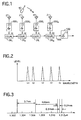
- the present invention relates to a fiber optics transmission system which transmits radio signals over optical fiber lines and, more particularly, to a fiber optics transmission system which is used to build mobile communication systems in underground shopping malls, tunnels and similar radio dead zones.
- radio access units 200 1 to 100 N are connected via optical couplers 26 1 to 26 N to an optical fiber line 300, which is, in turn, connected to a base unit 100.
- Radio frequency signals (hereinafter referred to as RF signals) received by antennas 21 of the radio access units 200 1 to 200 N are fed to semiconductor laser devices 25, each formed by a laser diode, in the access units, wherein the received RF signals are used to intensity-modulate laser light of wavelengths ⁇ 1 to ⁇ N emitted from the laser diodes.
- the optical signals of the wavelengths ⁇ 1 to ⁇ N from the access units 200 1 to 200 N are each provided via an optical coupler onto the optical fiber line 300 and combined with other optical signals one after another, and the combined light is fed to a photodiode 11 of the base unit 100.
- the photodiode 11 converts the combined light into radio-frequency signals corresponding to the intensity-modulated components of the respective wavelengths, and the base unit 100 sends the radio-frequency signals to base stations not shown.
- the oscillation frequencies of the laser diodes of the access units 200 1 to 200 N are chosen so that they are spaced apart to prevent the generation of beat noise by wavelength differences in the working radio-frequency band.
- the optical signals of the wavelengths ⁇ 1 to ⁇ N are provided onto the optical fiber line 300 and combined with one another and the combined optical signal is fed to the photodiode 11 of the base unit 100, so that the beat noise is generated which results from wavelength differences among the optical signals sent from the radio access units 200 1 to 200 N .
- the semiconductor laser devices 25 of the access units 200 1 to 200 N each oscillate laser light of a 1.3- ⁇ m band and that the wavelength difference between two optical signals is about 0.005 nm
- the beat frequency is around 1 GHz, which falls in the using radio frequency band.
- the actual oscillation wavelengths of such laser diodes vary, even if in the same wavelength band, because of various kinds of variations occurring in their manufacturing process.
- the oscillation wavelengths of commercially available 1.3- ⁇ m band laser diodes vary in the range of from 1.300 to 1.314 ⁇ m.
- a set of laser diodes of wavelength spacing greater than a predetermined value are selected from a large number of purchased laser diodes and the selected laser diodes are assigned to the units 2001 to 200N to construct the fiber optics transmission system depicted in Fig. 1.
- the radio access units 2001 to 200N are placed in different temperature environments.
- the oscillation wavelength of the laser diode varies with temperature; the wavelength deviates approximately 0.2 to 0.5 nm from the center wavelength at 0 to 5°C.
- the oscillation wavelength vs. temperature characteristic of the laser diode varies with aging as well.
- the oscillation wavelengths of the laser diodes in some of the radio access units 2001 to 200N come close to adjacent ones of them because of a temperature change and/or aging as shown in Fig. 3, resulting in the beat noise being generated in the radio signal transmission band.
- the generation of such beat noise in the radio signal transmission band will seriously degrade the C/N characteristic.
- EP-A-0 591 961 discloses a system in accordance with the pre-characterizing portion of claim 1, in which each radio access unit has a light mixing part to mix its own output light with that of another radio access unit, a detecting part for detecting beat noise in the output of the mixing part and a feedback loop for controlling the carrier frequency of its own output light so as to avoid beat noise.
- each radio access unit needs its own beat noise detector.
- US-A-4,916,460 discloses a system in accordance with the pre-characterizing portion of claim 1 but does not provide any measures against beat noise.
- the present invention has for its object the provision of a fiber optics transmission system which permits the use of arbitrarily selected commercially available laser diodes in respective access units regardless of temperatures of their use environments and the oscillation wavelength characteristics of the individual laser diodes and which automatically reduces the beat noise.
- the N radio access units each repeat independently selecting, based on the random value, the wavelength of the up-link optical signal to be provided onto the up-link optical fiber line, by which automatic control is effected to reduce the beat noise.
- the fiber optics transmission system of the present invention is made up of a base unit 100, N radio access units 200 1 , 200 2 , ..., 200 N and a pair of optical fiber lines 300 U (up-link) and 300 D (down-link).
- the radio access units 200 1 to 200 N and the base unit 100 are cascade-connected via the two optical fiber lines 300 U and 300 D .
- the base unit 100 is connected via a radio transmission channel to one of base stations of a mobile communication system.
- the radio access units 2001 to 200N are installed at intervals of 50 to 100 m in an underground shopping mall, for instance.
- An up-link radio signal RF U transmitted from a portable telephone or the like in the underground shopping mall is received by an antenna 21 of the nearest radio access unit, for example, 200 1 and is converted into an up-link optical signal PL U by a semiconductor laser device 25 formed by a laser diode.
- the up-link optical signal PL U is intensity-modulated by an up-link radio signal.
- the up-link optical signal PL U is coupled by an optical coupler 26 to the up-link optical fiber line 300 U .
- the base unit 100 receives combined light from the N radio access units 200 1 to 200 N and collectively recovers therefrom up-link radio signals by means of a photodiode 11. In this way, the up-link radio signal is sent to a control station (the base station, for instance).
- a down-link radio signal generated in the control station is converted by the semiconductor laser device in the base unit 100 into a down-link optical signal for transmission to the radio access units 200 1 to 200 N .
- the down-link optical signal is sent to each of the radio access units 200 1 to 200 N over the down-link optical fiber line 300 D .
- the radio access units 200 1 to 200 N each distribute the down-link optical signal by an optical coupler 27 inserted in the down-link optical fiber line 300 D .
- a down-link radio signal RF D is recovered by a photodiode 28 from the down-link optical signal, which is transmitted via the antenna 21.
- Reference numeral 22 denotes a duplexer for using the antenna 21 for both of transmission and reception
- 23, 24 and 13, 14 denote bias circuits which provide bias currents for driving the semiconductor laser devices 12 and 25 and combiner circuits for modulating the bias currents by radio signals.
- the photodiode of the base unit 100 receives the combined light signal of the optical signals from the access units 200 1 to 200 N and converts it into an up-link radio signal of the radio transmission band; when a beat falling in the working radio transmission band is generated due to a difference between laser oscillation wavelengths in two access units, the base unit 100 detects it and sends the detection signal to the respective access units 2001 to 200 N , each of which repeats randomly changing the laser oscillation wavelength independently of the others until the beat detection signal disappears.
- the base unit 100 is provided with a distribution circuit 15, a noise detector 16, a comparator 17 and a noise information generating section 18, and the radio access units 2001 to 200N are each provided with a distribution circuit 29, a noise information detector 31, a random signal generator 32 and a wavelength control circuit 33.
- the distribution circuit 15 in the base unit 100 distributes the up-link radio signal from the photodiode 11 to the control station side and the noise detector 16.
- the noise detector 16 can be formed by a cascade-connection of a band-pass filter 16A, an amplifier 16B, a diode detector 16C and a low-pass filter 16D.
- the pass band of the band-pass filter 16A is chosen to be a noise detecting band 6b set up in the proximity of a radio signal transmission band 6a. With the pass band of the band-pass filter chosen outside the radio signal transmission band, it is possible to detect the beat noise independently of the up-link radio signal.
- the oscillation wavelengths of the laser diodes 25 vary with an ambient temperature change or aging and when the oscillation wavelengths of the laser diodes in two radio access units become close to each other, the beat noise is generated in the radio signal transmission band.
- the oscillation wavelengths of the up-link optical signals PL 2 and PL 3 generated in the radio access units 200 2 and 200 3 come close to each other as depicted in Fig. 7, noise will increase over the entire radio signal transmission band as shown in Fig. 6 when the up-link optical signals are converted by the photodiode 11 of the base unit 100 into radio signals.
- the oscillation spectra of the laser diodes spread as indicated by PL 1 to PL 5 in Fig. 7.
- the frequency component 6c of the resulting beat noise is distributed over a wide band including the working radio signal transmission band 6a as shown in Fig. 6.
- the beat noise can be detected by the detection of the noise level in the frequency band adjacent the radio signal transmission band in the base unit 100.
- the level of the beat noise 6c is shown to drop at about 10 GHz--this means that the response frequency of the photodiode 11 is up to around 10 GHz.
- a noise level signal from the noise detector 16 is compared by the comparator 17 with a reference value P RN .
- the comparator 17 When the noise level is higher than the reference value P RN , the comparator 17 generates, for example, an H-logic detection signal, which is fed to the noise information generating section 18 to start it.
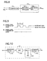
- the noise information generating section 18 is, in this example, made up of a rectangular wave generator 18A and a sine wave generator 18B as shown in Fig. 8.
- the rectangular wave generator 18A generates a rectangular wave of a period T shown in Fig. 9 Row A.
- the period T is chosen longer than a time constant for a temperature-oscillation wavelength variation of the laser diode 25 in each of the radio access units 200 1 to 200 N .
- the meaning of such a choice of the period T will become apparent from the description given later on of the operation of a wavelength control circuit 33.
- the sine wave generator 18B generates a sine wave, for example, only while the rectangular wave generator 18A yields the H-logic output, and hence it intermittently outputs the sine wave as noise information S N .
- Fig. 9 Row B shows the output from the rectangular wave generator 18A when the noise level is lower than the reference value P RN .
- the noise information signal SN thus generated in the noise information generating section 18 is combined with a down-link radio signal that is sent from the control station side to the combiner 13, and the combined signal is used to intensity-modulate a bias current I B being applied from the bias circuit 14 to the semiconductor laser device 12.
- the optical signal thus added with the noise information signal S N is sent onto the down-link optical fiber line 300 D .
- the radio access units 200 1 to 200 N each branch the down-link optical signal sent over the down-link optical fiber line 300 D by the down-link optical coupler 27 and converts it by the photodiode 28 into a radio signal and the noise information signal.
- the radio signal thus converted by the photodiode 28 is fed by the distribution circuit 29 to the duplexer 22 and transmitted as the down-link radio signal RF D via the antenna 21.
- the noise information signal converted by the photodiode 28 is fed to the noise information detector 31, by which the presence or absence of the noise information S N is always monitored.
- the noise information detector 31 can be formed, for example, by a cascade connection of a band-pass filter 31A, an amplifier 31B, a diode detector 31C and a low-pass filter 31D as shown in Fig. 10.
- the center frequency of the band-pass filter 31A is chosen to be the same as the frequency of the sine wave that is generated by the sine wave generator 18B in the noise information generating section 18 of the base unit 100. Accordingly, when intermittently supplied with the noise information S N , the band-pass filter 31A intermittently outputs the sine-wave signal corresponding to the noise information.
- the sine-wave signal is amplified by the amplifier 31B up to a required level and detected by the diode detector 31C and the detected output is taken out via the low-pass filter 31D, by which is recovered at the output of the low-pass filter 31D a rectangular wave of the same period T as that of the rectangular wave (Fig. 9 Row A) that is generated by the rectangular generator 18A in the noise information generating section 18 of the base unit 100.
- the thus recovered rectangular wave is fed to the random signal generator 32.
- the noise information detector 31 outputs a rectangular wave Tr representing noise information "present”
- the random signal generator 32 is triggered, for example, upon each rise of the rectangular wave, repeating updating the random value.
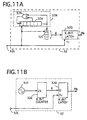
- the random signal generator 32 has, for example, a pseudo-random sequence generator 32R made up of an M-bit shift register 32A which is shifted one bit upon each rise of the recovered rectangular wave fed to a terminal 32L and a feedback gate circuit (an exclusive OR circuit) 32B as shown in Fig. 11A. Each bit of the pseudo-random sequence that is generated by the pseudo-random sequence generator 32R is taken in a K-bit shift register 32C upon each rise of the rectangular wave.
- a pseudo-random sequence generator 32R made up of an M-bit shift register 32A which is shifted one bit upon each rise of the recovered rectangular wave fed to a terminal 32L and a feedback gate circuit (an exclusive OR circuit) 32B as shown in Fig. 11A.
- Each bit of the pseudo-random sequence that is generated by the pseudo-random sequence generator 32R is taken in a K-bit shift register 32C upon each rise of the rectangular wave.
- a K-bit latch circuit 32D latches, as a parallel signal, a random signal of K bits from K shift stages of the K-bit shift register 32C upon each rise of the rectangular wave signal Tr. Consequently, when the generation of the beat noise in the working radio transmission band is detected at the base unit 100 side, the rectangular wave Tr is fed to a trigger terminal of the K-bit latch circuit 32D during the detection of the beat noise, whereby the value of the random signal is updated every period T of the rectangular wave.
- the parallel K-bit signal latched by the random signal generator 32 is provided as a random value M R to the wavelength control circuit 33.
- the random signal generator 32 is shown to be formed using a known pseudo-random sequence generator, it can also be formed in such a simpler configuration as shown in Fig. 11B. That is, the random signal generators 32 of the respective access units 200 1 to 200 N are provided with clock generators 32F which generate clock signals of periods shorter than that T of the rectangular wave signal and of different clock frequencies f C1 , f C2 , ..., F CN . The clock signals that are generated by the clock generator 32F in each access unit are counted by a K-bit counter 32E at all times.
- the K-bit latch 32D latches the count value of the K-bit counter 32E upon each rise of the rectangular wave and provides it as the random value M R to the wavelength control circuit 33.
- the period of the rectangular wave signal used as a trigger signal for the latch 32D and the period of the clock signal generated by the clock generator 32F are asynchronous to each other, so that the K-bit count value, which is latched upon each rise of the rectangular wave, can be regarded as a random value.
- the oscillation wavelength of the laser diode can be set to a desired value by a method according to which a heat source element capable of generating and absorbing heat, such as a Peltier element, is controlled by the wavelength control circuit 33 to directly vary the temperature of the laser diode of the laser device in Fig. 4 to set its oscillation wavelength to an arbitrary value, or a method according to which the bias circuit 24 is controlled by the wavelength control circuit 33 as indicated by the broken line to vary the bias current I B to be fed to the laser diode to set its oscillation wavelength to a desired value.
- a heat source element capable of generating and absorbing heat such as a Peltier element
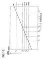
- Fig. 12 is a schematic graph showing the relationship between temperature and wavelength represented on the abscissa and the left-hand ordinate, respectively.
- T 1 to T J are determined for each laser diode at intervals such that beats by adjacent oscillation wavelengths at these temperatures do not fall in the working radio transmission band.
- Random values M R corresponding to such J temperatures are determined as indicated on the right-hand ordinate of the graph in Fig. 12.
- the random values M R need only to have a one-to-one correspondence with the temperatures T i and their magnitudes may be arbitrarily sequenced.
- the wavelength control circuit 33 in each access unit selects that one of the J temperature values T 1 to T J which corresponds to the random value M R and controls the laser diode in that access unit to reach the selected temperature.
- Fig. 13 illustrates an example of the wavelength control circuit 33 which uses a heat source element to control the temperature of the semiconductor laser device 25 to set the laser oscillation wavelength at an arbitrary value.
- the laser device 25 is made up of a laser diode 25A mounted on a base plate 25B of high thermal conductivity, a heat source element 25C closely contacted with the base plate 25B, and a temperature sensor 25D mounted on the base plate in proximity of the laser diode 25A.
- the wavelength control circuit 33 comprises a reference temperature setting circuit 33A and a heat source element control circuit 33B.
- the heat source element control circuit 33B controls the heat generating (heat absorbing) temperature of the heat source element 25C such as a Peltier element.
- the heat source element control circuit 33B compares the temperature value T i thus fed thereto and the temperature of the laser diode 25A detected by the temperature sensor 25D and effects automatic control for controlling the temperature of the heat source element 25C to keep the temperature of the laser diode 25A equal to the temperature value Ti.
- the reference temperature T i set by the reference temperature setting circuit 33A is updated with a value corresponding to the random value M R that is provided from the random signal generator 32 with the period T of the rectangular wave. Since the period T is set to a time (about one minute, for instance) longer than the time constant of the temperature-oscillation wavelength change of each laser diode 25A as described previously herein, the temperatures of the laser diodes 25A change to the reference temperatures Ti randomly set by the reference temperature setting circuits 33A in the access units 200 1 to 200 N and when the beat noise is no longer detected at the base unit 100 side as the result of the laser oscillation wavelengths having changed to the newly set wavelengths, the generation of the noise information is stopped and the updating of the random signals M R is also stopped. When the beat noise is still detected, the noise information is sent from the base unit 100 side correspondingly and the random signal updating operation is repeated.
- the temperature of the laser diode is controlled through utilization of the linear relationship between temperature and the laser oscillation wavelength shown in Fig. 12.
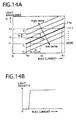
- the oscillation wavelength of the laser diode and the bias current bear substantially a linear relationship as indicated by the thick line 14a in Fig. 14A when temperature is constant.
- the bias current range from I B1 to I BJ which spans J wavelengths ⁇ 1 to ⁇ J distributed over the wavelength range covered by the thick straight line, is set starting at a bias current at which the bias current vs.
- the bias current range is divided into 15 sections, for which bias current values I B1 , I B2 , ..., I BJ are predetermined, and random values "0000" to "1111” are made to correspond to the bias current values, respectively.
- Fig. 15 there is illustrated the configurations of the wavelength control circuit 33 and the semiconductor laser device 25 in the case of controlling the laser oscillation wavelength through control of the bias current. In this example, however, they are so configured as to suppress temperature variations of the laser diode which would otherwise cause wavelength variations.
- the wavelength control circuit 33 has a reference current setting circuit 33C and a compensating circuit 33D, whereas the semiconductor laser device 25 has a substrate 25B and a laser diode 25A and a temperature sensor 25D both mounted thereon.
- the reference current setting circuit 33C has a conversion table which represents the relationships between the J random values M R from "0000" to "1111" predetermined in a one-to-one correspondence with the J wavelengths ⁇ 1 to ⁇ J distributed over the predetermined wavelength range and the bias currents I B1 to I BJ corresponding to the random values, respectively; the reference current setting circuit provides, as a reference current value, the bias current value (an analog value) I Bi corresponding to the random value M R thereto to the compensating circuit 33D.
- the compensating circuit 33D is made up of an operational amplifier 33D1 and an adder 33D2 as shown in Fig. 16.
- the operational amplifier 33D2 formed by an inverting amplifier, has its gain set at -0.01 nm/10°C when the oscillation wavelength of the laser diode 25A changes at a rate of +0.01 nm/10°C, for instance.
- the detected temperature S T from the temperature sensor 25D is input into the operational amplifier 33D1, in which it is inverted and amplified with the preset gain, thereafter being applied to the adder 33D2 for addition with the reference current I Bi from the reference current setting circuit 33C. Consequently, the adder 33D2 subtracts from the reference current value I Bi a value proportional to the temperature of the laser diode 25A.
- the bias current is so adjusted as to suppress variations in the laser oscillation wavelength attributable to temperature changes of the laser diode. For example, when the oscillation wavelength increases with an increase in ambient temperature, the bias current is controlled to reduce the oscillation wavelength.
- the output C B from the adder 33D2 is provided as a temperature-compensated reference current value to the bias circuit 24 (Fig. 4), which supplies the laser diode 25A with a bias current corresponding to the reference current value.
- the compensating circuit 33D in Fig. 15 may also be formed using an AD converter 33D3, a ROM table 33D4 formed by a ROM, a DA converter 33D5 and a subtractor 33D2 as depicted in Fig. 17. While the bias current and the laser oscillation wavelength bear substantially a linear relationship as shown in Fig. 14A, the straight line representing relationship will translate when the temperature changes. Now, let it be assumed that the reference temperature T R is, for example, 25°C and that the straight line representing the bias current vs. oscillation wavelength characteristic at that temperature is the thick line 14a in Fig. 14A.
- the oscillation wavelength becomes longer than ⁇ i by ⁇ as shown in Fig. 14A. Hence, the oscillation wavelength can be corrected to ⁇ i by decreasing the bias current I Bi by ⁇ I.
- ⁇ T/ ⁇ I corresponds to the gradient ⁇ / ⁇ I of the straight line and is constant.
- the oscillation wavelength of the laser diode can always be corrected to the same wavelength as that ⁇ i at the reference temperature T R .
- T R and K are predetermined values, the amount of correction of the bias current, ⁇ I, will unequivocally be determined when the temperature sensor output S T is provided.
- the ROM table 33D4 in the compensating circuit 33D of Fig. 17 there are written the amounts of correction of the bias current ⁇ I corresponding to individual values of the sensor output S T used as addresses; the amount of correction ⁇ I corresponding to the input value S T can be read out of the ROM table.
- the detected temperature S T by the temperature sensor 25D is converted by the AD converter 33D3 into a digital value, which is fed to as an address to the ROM table 33D4 to read out therefrom the corresponding amount of correction ⁇ I.
- the amount of correction ⁇ I thus read out of the ROM table is converted by the DA converter 33D5 into an analog value, which is subtracted by the subtractor 33D2 from the preset bias current value I Bi to obtain a corrected bias current value.
- the corrected bias current value thus obtained is provided to the bias circuit 24, which generates the corresponding bias current.
- the subtractor 33D2 may be interposed between the ROM table 33D4 and the DA converter 33D5 to perform a digital subtraction.
- the reference current setting circuit 33C outputs a digital reference current value I Bi corresponding to the random value M R .
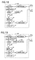
- Fig. 18 illustrates a modified form of the base unit 100.
- the base unit 100 is provided with a clock circuit 19C, which is used to perform the above-described calibrating operation in a time period of the lowest traffic of use of the mobile communication system, for instance.
- the clock circuit 19C outputs an H-logic signal during a time zone from twelve to one o'clock midnight, for instance, to enable a gate circuit 19A to permit the passage therethrough of the detected output from the noise detector 16, performing the calibration only while the gate circuit 19A remains enabled.
- Fig. 19 illustrates another embodiment of the base unit 100.
- the clock circuit 19A in Fig. 18 is substituted with a radio signal detector 19D, which enables the gate circuit 19A only in the absence of radio signals, allowing the calibrating operation to take place. Accordingly, in this instance, the calibration is performed while no communication is being carried out, so that it is possible to maintain a highly reliable communication system which does not inconvenience users by the calibration.
- the noise information generating section 18 in the base unit 100 has been described to include the rectangular wave generator 18A (Fig. 8), it is not always necessary. That is, the noise information generating section 18 can be formed by only the sine wave generator 18B, in which case sine-wave noise information is continuously generated upon detection of the beat noise by the noise detector 16. In this instance, the noise information detector 31 (Fig. 10) of each access unit 200 i outputs a continuous "H" level.
- a rectangular wave generator 31E is provided, as depicted in Fig. 20, at the output side of the low-pass filter 31D in the noise information detector 31 of each radio access unit 200 i shown in Fig. 10.
- the detection signal "H” is applied to the rectangular wave generator 31E to cause it to generate the rectangular signal of the period T, which is fed to the random signal generator 32.
- N evenly spaced temperature values are predetermined for each laser diode so that they provide a wavelength spacing ⁇ greater than the wavelength difference lest the beat noise should fall in the radio transmission band.
- each access unit repeats randomly selecting any one of the N temperature values (or bias current values) and setting the laser diode of the semiconductor laser device at the selected temperature (or bias current).
- the wavelengths of optical signals generated by the respective access units are certain to exceeds the predetermined wavelength spacing ⁇ .
- the number N of access units needed in a medium-sized underground shopping mall, for instance, is four or five at the greatest.
- each access units Upon detection of the beat noise, each access units begins to repeat random selection of the laser oscillation wavelength and the beat noise is reduced within several minutes at the longest. With such a configuration, it is unnecessary, in the construction of an optical transmission system, to measure the oscillation wavelength characteristics of a lot of purchased laser diodes so as to select those which are used in the respective access units.
- the beat noise resulting from the change in the oscillation wavelength is detected and the noise information is sent to the radio access units 200 1 to 200 N over the down-link optical fiber line 300D.
- the noise information is used to update the random value that is provided from the random signal generator 32 in each of the radio access unit and the random value is used to change the laser diode 25A.
Landscapes
- Engineering & Computer Science (AREA)
- Physics & Mathematics (AREA)
- Electromagnetism (AREA)
- Computer Networks & Wireless Communication (AREA)
- Signal Processing (AREA)
- Computing Systems (AREA)
- Optical Communication System (AREA)
Claims (11)
- Faseroptisches Übertragungssystem, welches folgendes umfasst:dadurch gekennzeichnet, dassN Funkzugangseinheiten (261 - 26N, 2001 - 200N), von denen jede ein erstes Uplink-Funksignal (RFU) eines Mobilfunkgeräts, das von einer Antenne (21) empfangen wird, in ein optisches Uplink-Signal unter Verwendung einer Halbleiterlaservorrichtung (25) umwandelt, ein optisches Downlink-Signal in ein erstes Downlink-Funksignal (RSD) unter Verwendung einer ersten Fotodiode (28) umwandelt und es über die Antenne (21) zum Mobilfunkgerät überträgt, wobei N eine ganze Zahl ist, die gleich oder größer ist als 2;optische Uplink- und Downlink-Faserleitungen (300U, 300D), mit welchen die N Funkzugangseinheiten (261 - 26N, 2001 - 200N) in Kaskade verbunden sind; undeine Basiseinheit (100), welche ein zweites Downlink-Funksignal, das von einer Steuerstation empfangen wird, in ein optisches Downlink-Signal umwandelt und es auf der optischen Downlink-Faserleitung (300D) bereitstellt und ein optisches Uplink-Signal, das von der optischen Uplink-Faserleitung (300U) empfangen wird, in ein zweites Uplink-Funksignal umwandelt und es an die Steuerstation überträgt;
die Basiseinheit (100) ein Rauscherfassungsmittel (16, 17) zum Erfassen von Schwebungsrauschen im zweiten Uplink-Funksignal und ein Rauschinformationserzeugungsmittel (18) zum Erzeugen von Rauschinformation, welche das Vorhandensein von Schwebungsrauschen während dessen Erkennung repräsentiert, und Senden dieser Rauschinformation an die N Funkzugangseinheiten (2001 - 200N) über die optische Downlink-Faserleitung (300D) umfasst; und
dass jede der Funkzugangseinheiten (2001 - 200N) umfasst: ein Zufallssignalerzeugungsmittel (31, 32) zum wiederholten Erzeugen eines Zufallswerts während des Vorhandenseins der Rauschinformation und eine Wellenlängensteuerungsschaltung (33) zum Steuern der Halbleiterlaservorrichtung (25), um zufällig gemäß dem Zufallswert eine von wenigstens N Wellenlängen auszuwählen, die um einen vorbestimmten Wert oder mehr voneinander beabstandet sind. - System nach Anspruch 1, bei dem die Basiseinheit (100) folgendes umfasst:wobei jede Funkzugangseinheit (2001 - 200N) weiterhin umfasst:eine zweite Fotodiode (11), die das optische Uplink-Signal auf der optischen Uplink-Faserleitung (300U) in das zweite Uplink-Funksignal umwandelt;besagtes Rauscherfassungsmittel (16), das angepasst ist, einen Rauschpegel in der Ausgabe der zweiten Fotodiode (11) zu erkennen und zu bestimmen, ob dieser Rauschpegel höher als ein vorgegebener Pegel ist;besagtes Rauschinformationserzeugungsmittel (18), das angepasst ist, besagte Rauschinformation zu erzeugen, während bestimmt wird, dass der Rauschpegel höher ist als der vorbestimmte;eine erste Laserdiode (12), welche Licht zur Bereitstellung auf der optischen Downlink-Faserleitung (300D) emittiert;eine ersten Vorspannungsschaltung (14), um einen Vorspannungsstrom an die erste Laserdiode (12) anzulegen; undeine erste Kombinierschaltung (13), um den Vorspannungsstrom von der ersten Vorspannungsschaltung (14) an die erste Laserdiode (12) mit dem zweiten Downlink-Funksignal und der Rauschinformation in der Intensität zu modulieren, und den intensitätsmodulierten Vorspannungsstrom an die erste Laserdiode (12) anzulegen;wobei die erste Fotodiode (28) angepasst ist, um das optische Downlink-Signal zu empfangen, das vom optischen Downlink-Koppler verteilt wird, und es in das erste Downlink-Funksignal zu konvertieren; undeinen optischen Downlink-Koppler (27), der in die optische Downlink-Faserieitung (300D) eingesetzt ist, um ein optisches Downlink-Signal zu verteilen;einen optischen Uplink-Koppler (26), der in die optische Uplink-Faserleitung (300U) eingefügt ist, um die Halbleiterlaservorrichtung (25) mit dem optischen Uplink-Koppler (26) optisch zu koppeln;eine zweite Vorspannungsschaltung (24), um einen Vorspannungsstrom an die Halbleiterlaservorrichtung (25) anzulegen, um sie in Oszillation zu versetzen; undeine zweite Kombinierschaltung (23), um den Vorspannungsstrom von der zweiten Vorspannungsschaltung (24) mit dem ersten Uplink-Funksignal in der Intensität zu modulieren und um den intensitätsmodulierten Vorspannungsstrom an die Halbleiterlaservorrichtung (25) anzulegen;
wobei das Zufallssignalerzeugungsmittel (31, 32) folgendes umfasst:wobei die Wellenlängensteuerungsschaltung (33) angepasst ist, um die Oszillationswellenlänge der Halbleiterlaservorrichtung (25) in Übereinstimmung mit dem von dem Zufallsignalgenerator gehaltenen Zufallswert zu steuern.einen Rauschinformationsdetektor (31), der mit dem ersten Downlink-Funksignal von der ersten Fotodiode (28) versorgt wird, um die Rauschinformation in dem ersten Downlink-Funksignal zu erfassen; undeinen Zufallsignalgenerator (32), um während der Erfassung der Rauschinformation durch den Rauschinformationsdetektor (31) wenigstens N Zufallswerte entsprechend wenigstens N Wellenlängen mit einem vorbestimmten Abstand zu erzeugen, und um die N Zufallswerte mit einer vorbestimmten Periode zu aktualisieren und zu halten; - System nach Anspruch 1 oder 2, bei dem die Basiseinheit (100) eine Uhrenschaltung (19C) umfasst, welche die Erzeugung der Rauschinformation nur in einer vorgegebenen Zeitzone erlaubt.
- System nach Anspruch 1 oder 2, bei dem die Basiseinheit (100) einen Funksignalgenerator (19D) zum Erfassen eines Nichtvorhandenseins des Funksignals von der zweiten Fotodiode (11) und zum Erlauben der Erzeugung der Rauschinformation durch ein Nichtvorhandensein des Schwebungsrauschens umfasst.
- System nach einem der Ansprüche 1 oder 2, bei dem die Halbleiterlaservorrichtung (25) jeder Funkzugangseinheit (2001 - 200N) eine zweite Laserdiode (25A), die mit dem optischen Uplink-Koppler (26) optisch gekoppelt ist, ein Wärmequellenelement (25C), das in der Lage ist, Wärme zu erzeugen und zu absorbieren und thermisch mit der zweiten Laserdiode (25A) verbunden ist, und einen Temperatursensor (25D) zum Erfassen der Temperatur der zweiten Laserdiode (25) umfasst, und die Wellenlängensteuerungsschaltung (33) eine Referenztemperatursetzschaltung (33A) zum Auswählen eines von wenigstens N Temperaturwerten, die jeweils den wenigstens N Wellenlängen entsprechen, anhand des Zufallswertes und zum Ausgeben des ausgewählten Temperaturwerts als einen Referenztemperaturwert und eine Wärmequellenelementsteuerungsschaltung (33B) umfasst, um diesen Referenztemperaturwert in Übereinstimmung mit der durch den Temperatursensor erfassten Temperatur der zweiten Laserdiode (25A) zu korrigieren, und um diesen korrigierten Referenztemperaturwert an das Wärmequellenelement (25C) zu liefern, um dessen Temperatur zu steuern.
- System nach Anspruch 5, bei dem die Anzahl der Temperaturwerte größer ist als N.
- System nach einem der Ansprüche 1 oder 2, bei dem die Halbleiterlaservorrichtung (25) jeder Funkzugangseinheit (2001 - 200N) eine zweite Laserdiode (25A) umfasst, die optisch mit dem optischen Uplink-Koppler (26) gekoppelt ist, und einen Temperatursensor (25D) umfasst, um die Temperatur der zweiten Laserdiode (25A) zu erkennen, und die Wellenlängensteuerungsschaltung (33) eine Referenzstromsetzschaltung (33C), um anhand des Zufallswertes einen von wenigstens N Vorspannungsströmen, die jeweils den wenigstens N Wellenlängen entsprechen, auszuwählen und um diesen ausgewählten Vorspannungsstromwert als einen Referenzstromwert auszugeben, und eine Kompensationsschaltung (33D) umfasst, die mit diesem Referenzstromwert versorgt wird, um ihn in Übereinstimmung mit der durch den Temperatursensor erfassten Temperatur der zweiten Laserdiode (25A) zu korrigieren, und um diesen korrigierten Referenzstromwert an die Vorspannungsschaltung (24) zu liefern.
- System nach Anspruch 7, bei dem die Anzahl der Referenzstromwerte größer ist als N.
- System nach Anspruch 7, bei dem die Kompensationsschaltung (33D) folgendes umfasst:einen AD-Wandler (33D3), um die Temperatur, die vom Temperatursensor (25D) erfasst wird, in einen digitalen Wert umzuwandeln;einen Speicher (33D4), in den Vorspannungskorrekturgrößen in einer eindeutigen Entsprechung mit vorbestimmten Temperaturwerten eingeschrieben sind; undeinen Subtrahierer (33D2), um die aus dem Speicher (33D4) ausgelesenen Vorspannungskorrekturgrößen von dem ausgewählten Referenzstromwert abzuziehen und sie als einen korrigierten Referenzvorspannungsstromwert an die Vorspannungsschaltung (24) zu liefern.
- System nach Anspruch 2, bei dem der Zufallsignalgenerator (32) folgendes umfasst:einen Pseudozufallssequenzgenerator (32R) zum Erzeugen einer Pseudozufallssequenz, der durch ein Rechteckwellensignal angetrieben wird, welches das vom Rauschinformationsdetektor (31) erfasste Vorhandensein von Schwebungsrauschen anzeigt;ein Schieberegister (32C) mit wenigstens K Schiebestufen, das mit der Pseudozufallssequenz in Synchronisation mit dem Rechteckwellensignal versorgt wird; undeine Verriegelungsschaltung (32D), um darin K parallele Bits von den K Schiebestufen des Schieberegisters (32C) in Synchronisation mit dem Rechteckwellensignal zu verriegeln, wobei K diejenige kleinste ganze Zahl ist, welche 2K-1≥J erfüllt, und J die für jede der Laserdioden wählbare Anzahl von Oszillationswellenlängen ist.
- System nach Anspruch 2, bei dem der Zufallsignalgenerator (32) jeder Funkzugangseinheit (2001 - 200N) einen Taktgenerator (32F) hat, um Taktsignale mit verschiedenen Taktperioden zu erzeugen, die kürzer sind als die Periode des Rechteckwellensignals, einen K-bit-Zähler (32E), um Taktsignale vom Taktgenerator zu zählen, und eine K-bit-Verriegelungsschaltung (32D), um darin den Zählwert des K-bit-Zählers (32E) in Synchronisation mit dem Rechteckwellensignal zu verriegeln, wobei K diejenige kleinste ganze Zahl ist, welche 2K-1≥J erfüllt, und das J die für jede der Laserdioden wählbare Anzahl von Oszillationswellenlängen ist.
Applications Claiming Priority (7)
| Application Number | Priority Date | Filing Date | Title |
|---|---|---|---|
| JP214550/95 | 1995-08-23 | ||
| JP21455095 | 1995-08-23 | ||
| JP21455095 | 1995-08-23 | ||
| JP15101496 | 1996-06-12 | ||
| JP151014/96 | 1996-06-12 | ||
| JP15101496 | 1996-06-12 | ||
| PCT/JP1996/002340 WO1997008856A1 (en) | 1995-08-23 | 1996-08-22 | Optical fiber transmission system |
Publications (3)
| Publication Number | Publication Date |
|---|---|
| EP0805569A1 EP0805569A1 (de) | 1997-11-05 |
| EP0805569A4 EP0805569A4 (de) | 1998-12-23 |
| EP0805569B1 true EP0805569B1 (de) | 2004-04-21 |
Family
ID=26480416
Family Applications (1)
| Application Number | Title | Priority Date | Filing Date |
|---|---|---|---|
| EP96927869A Expired - Lifetime EP0805569B1 (de) | 1995-08-23 | 1996-08-22 | Faseroptisches übertragungssystem |
Country Status (5)
| Country | Link |
|---|---|
| US (1) | US5812296A (de) |
| EP (1) | EP0805569B1 (de) |
| JP (1) | JP3096694B2 (de) |
| DE (1) | DE69632245T2 (de) |
| WO (1) | WO1997008856A1 (de) |
Families Citing this family (63)
| Publication number | Priority date | Publication date | Assignee | Title |
|---|---|---|---|---|
| JP3812787B2 (ja) * | 1997-11-20 | 2006-08-23 | 株式会社日立国際電気 | 光変換中継増幅システム |
| JP3974253B2 (ja) * | 1998-03-20 | 2007-09-12 | 株式会社東芝 | 光通信システムおよび光通信システムの制御方法 |
| KR100315705B1 (ko) * | 1998-10-22 | 2002-02-19 | 윤종용 | 파장분할다중광전송시스템의파장안정화장치 |
| KR100338623B1 (ko) | 2000-07-10 | 2002-05-30 | 윤종용 | 디지털 광 링크를 이용한 이동통신망 시스템 |
| EP1191697B1 (de) * | 2000-07-31 | 2011-12-21 | HILTI Aktiengesellschaft | Lokaloszillator zur Erzeugung eines HF-Signals zur Direktmischung mittels Avalanche-Fotodioden |
| DE60127791T2 (de) | 2000-10-25 | 2007-12-27 | Ntt Docomo Inc. | Übertragungssystem mit an optischen Fasern gekoppelten Funkeinheiten |
| JP2002246683A (ja) * | 2001-02-15 | 2002-08-30 | Toshiba Corp | 光送信器及び光伝送システム |
| JP2006171380A (ja) * | 2004-12-16 | 2006-06-29 | Sony Corp | ホログラム記録再生装置及びホログラム記録再生方法 |
| US20060133805A1 (en) * | 2004-12-16 | 2006-06-22 | Seung-Hyun Jang | Apparatus and method for detecting light source causing optical beat interference in subcarrier multiple access optical network |
| US7519329B2 (en) * | 2005-07-01 | 2009-04-14 | Research In Motion Limited | Determination of antenna noise temperature for handheld wireless devices |
| US7787823B2 (en) | 2006-09-15 | 2010-08-31 | Corning Cable Systems Llc | Radio-over-fiber (RoF) optical fiber cable system with transponder diversity and RoF wireless picocellular system using same |
| US7848654B2 (en) | 2006-09-28 | 2010-12-07 | Corning Cable Systems Llc | Radio-over-fiber (RoF) wireless picocellular system with combined picocells |
| US8873585B2 (en) | 2006-12-19 | 2014-10-28 | Corning Optical Communications Wireless Ltd | Distributed antenna system for MIMO technologies |
| US8111998B2 (en) | 2007-02-06 | 2012-02-07 | Corning Cable Systems Llc | Transponder systems and methods for radio-over-fiber (RoF) wireless picocellular systems |
| US20100054746A1 (en) | 2007-07-24 | 2010-03-04 | Eric Raymond Logan | Multi-port accumulator for radio-over-fiber (RoF) wireless picocellular systems |
| US8005358B2 (en) * | 2007-07-24 | 2011-08-23 | Tyco Electronics Subsea Communications Llc | System and method for suppressing beat noise in line monitoring equipment |
| US8175459B2 (en) * | 2007-10-12 | 2012-05-08 | Corning Cable Systems Llc | Hybrid wireless/wired RoF transponder and hybrid RoF communication system using same |
| WO2009081376A2 (en) | 2007-12-20 | 2009-07-02 | Mobileaccess Networks Ltd. | Extending outdoor location based services and applications into enclosed areas |
| DE102008013245A1 (de) * | 2008-03-08 | 2009-09-17 | Andrew Wireless Systems Gmbh | Repeater und Verfahren zum Betrieb eines solchen Repeaters |
| US9673904B2 (en) | 2009-02-03 | 2017-06-06 | Corning Optical Communications LLC | Optical fiber-based distributed antenna systems, components, and related methods for calibration thereof |
| WO2010090999A1 (en) | 2009-02-03 | 2010-08-12 | Corning Cable Systems Llc | Optical fiber-based distributed antenna systems, components, and related methods for monitoring and configuring thereof |
| JP5480916B2 (ja) | 2009-02-03 | 2014-04-23 | コーニング ケーブル システムズ リミテッド ライアビリティ カンパニー | 光ファイバベースの分散型アンテナシステム、構成要素、及びその較正のための関連の方法 |
| US9590733B2 (en) * | 2009-07-24 | 2017-03-07 | Corning Optical Communications LLC | Location tracking using fiber optic array cables and related systems and methods |
| US8548330B2 (en) | 2009-07-31 | 2013-10-01 | Corning Cable Systems Llc | Sectorization in distributed antenna systems, and related components and methods |
| US8280259B2 (en) | 2009-11-13 | 2012-10-02 | Corning Cable Systems Llc | Radio-over-fiber (RoF) system for protocol-independent wired and/or wireless communication |
| US8275265B2 (en) | 2010-02-15 | 2012-09-25 | Corning Cable Systems Llc | Dynamic cell bonding (DCB) for radio-over-fiber (RoF)-based networks and communication systems and related methods |
| US20110268446A1 (en) | 2010-05-02 | 2011-11-03 | Cune William P | Providing digital data services in optical fiber-based distributed radio frequency (rf) communications systems, and related components and methods |
| US9525488B2 (en) | 2010-05-02 | 2016-12-20 | Corning Optical Communications LLC | Digital data services and/or power distribution in optical fiber-based distributed communications systems providing digital data and radio frequency (RF) communications services, and related components and methods |
| EP2606707A1 (de) | 2010-08-16 | 2013-06-26 | Corning Cable Systems LLC | Remote-antennencluster und zugehörige systeme, bestandteile und verfahren zur unterstützung der signalverbreitung digitaler daten zwischen remote-antenneneinheiten |
| US9252874B2 (en) | 2010-10-13 | 2016-02-02 | Ccs Technology, Inc | Power management for remote antenna units in distributed antenna systems |
| CN203504582U (zh) | 2011-02-21 | 2014-03-26 | 康宁光缆系统有限责任公司 | 一种分布式天线系统及用于在其中分配电力的电源装置 |
| CN103609146B (zh) | 2011-04-29 | 2017-05-31 | 康宁光缆系统有限责任公司 | 用于增加分布式天线系统中的射频(rf)功率的系统、方法和装置 |
| EP2702710A4 (de) | 2011-04-29 | 2014-10-29 | Corning Cable Sys Llc | Bestimmung der weiterleitungsverzögerung von kommunikationen in verteilten antennensystemen sowie entsprechende komponenten, systeme und verfahren |
| WO2013148986A1 (en) | 2012-03-30 | 2013-10-03 | Corning Cable Systems Llc | Reducing location-dependent interference in distributed antenna systems operating in multiple-input, multiple-output (mimo) configuration, and related components, systems, and methods |
| EP2842245A1 (de) | 2012-04-25 | 2015-03-04 | Corning Optical Communications LLC | Verteilte antennensystemarchitekturen |
| WO2014024192A1 (en) | 2012-08-07 | 2014-02-13 | Corning Mobile Access Ltd. | Distribution of time-division multiplexed (tdm) management services in a distributed antenna system, and related components, systems, and methods |
| US8983304B2 (en) * | 2012-10-25 | 2015-03-17 | Avago Technologies General Ip (Singapore) Pte. Ltd. | Opto-isolator with compensation circuit |
| US9455784B2 (en) | 2012-10-31 | 2016-09-27 | Corning Optical Communications Wireless Ltd | Deployable wireless infrastructures and methods of deploying wireless infrastructures |
| CN105308876B (zh) | 2012-11-29 | 2018-06-22 | 康宁光电通信有限责任公司 | 分布式天线系统中的远程单元天线结合 |
| US9647758B2 (en) | 2012-11-30 | 2017-05-09 | Corning Optical Communications Wireless Ltd | Cabling connectivity monitoring and verification |
| WO2014199380A1 (en) | 2013-06-12 | 2014-12-18 | Corning Optical Communications Wireless, Ltd. | Time-division duplexing (tdd) in distributed communications systems, including distributed antenna systems (dass) |
| WO2014199384A1 (en) | 2013-06-12 | 2014-12-18 | Corning Optical Communications Wireless, Ltd. | Voltage controlled optical directional coupler |
| US9247543B2 (en) | 2013-07-23 | 2016-01-26 | Corning Optical Communications Wireless Ltd | Monitoring non-supported wireless spectrum within coverage areas of distributed antenna systems (DASs) |
| US9661781B2 (en) | 2013-07-31 | 2017-05-23 | Corning Optical Communications Wireless Ltd | Remote units for distributed communication systems and related installation methods and apparatuses |
| US9385810B2 (en) | 2013-09-30 | 2016-07-05 | Corning Optical Communications Wireless Ltd | Connection mapping in distributed communication systems |
| US9178635B2 (en) | 2014-01-03 | 2015-11-03 | Corning Optical Communications Wireless Ltd | Separation of communication signal sub-bands in distributed antenna systems (DASs) to reduce interference |
| US9775123B2 (en) | 2014-03-28 | 2017-09-26 | Corning Optical Communications Wireless Ltd. | Individualized gain control of uplink paths in remote units in a distributed antenna system (DAS) based on individual remote unit contribution to combined uplink power |
| US9357551B2 (en) | 2014-05-30 | 2016-05-31 | Corning Optical Communications Wireless Ltd | Systems and methods for simultaneous sampling of serial digital data streams from multiple analog-to-digital converters (ADCS), including in distributed antenna systems |
| US9525472B2 (en) | 2014-07-30 | 2016-12-20 | Corning Incorporated | Reducing location-dependent destructive interference in distributed antenna systems (DASS) operating in multiple-input, multiple-output (MIMO) configuration, and related components, systems, and methods |
| US9730228B2 (en) | 2014-08-29 | 2017-08-08 | Corning Optical Communications Wireless Ltd | Individualized gain control of remote uplink band paths in a remote unit in a distributed antenna system (DAS), based on combined uplink power level in the remote unit |
| US9602210B2 (en) | 2014-09-24 | 2017-03-21 | Corning Optical Communications Wireless Ltd | Flexible head-end chassis supporting automatic identification and interconnection of radio interface modules and optical interface modules in an optical fiber-based distributed antenna system (DAS) |
| US10659163B2 (en) | 2014-09-25 | 2020-05-19 | Corning Optical Communications LLC | Supporting analog remote antenna units (RAUs) in digital distributed antenna systems (DASs) using analog RAU digital adaptors |
| US9420542B2 (en) | 2014-09-25 | 2016-08-16 | Corning Optical Communications Wireless Ltd | System-wide uplink band gain control in a distributed antenna system (DAS), based on per band gain control of remote uplink paths in remote units |
| WO2016071902A1 (en) | 2014-11-03 | 2016-05-12 | Corning Optical Communications Wireless Ltd. | Multi-band monopole planar antennas configured to facilitate improved radio frequency (rf) isolation in multiple-input multiple-output (mimo) antenna arrangement |
| WO2016075696A1 (en) | 2014-11-13 | 2016-05-19 | Corning Optical Communications Wireless Ltd. | Analog distributed antenna systems (dass) supporting distribution of digital communications signals interfaced from a digital signal source and analog radio frequency (rf) communications signals |
| US9729267B2 (en) | 2014-12-11 | 2017-08-08 | Corning Optical Communications Wireless Ltd | Multiplexing two separate optical links with the same wavelength using asymmetric combining and splitting |
| WO2016098111A1 (en) | 2014-12-18 | 2016-06-23 | Corning Optical Communications Wireless Ltd. | Digital- analog interface modules (da!ms) for flexibly.distributing digital and/or analog communications signals in wide-area analog distributed antenna systems (dass) |
| WO2016098109A1 (en) | 2014-12-18 | 2016-06-23 | Corning Optical Communications Wireless Ltd. | Digital interface modules (dims) for flexibly distributing digital and/or analog communications signals in wide-area analog distributed antenna systems (dass) |
| US20160249365A1 (en) | 2015-02-19 | 2016-08-25 | Corning Optical Communications Wireless Ltd. | Offsetting unwanted downlink interference signals in an uplink path in a distributed antenna system (das) |
| US9681313B2 (en) | 2015-04-15 | 2017-06-13 | Corning Optical Communications Wireless Ltd | Optimizing remote antenna unit performance using an alternative data channel |
| US9948349B2 (en) | 2015-07-17 | 2018-04-17 | Corning Optical Communications Wireless Ltd | IOT automation and data collection system |
| US10560214B2 (en) | 2015-09-28 | 2020-02-11 | Corning Optical Communications LLC | Downlink and uplink communication path switching in a time-division duplex (TDD) distributed antenna system (DAS) |
| US10236924B2 (en) | 2016-03-31 | 2019-03-19 | Corning Optical Communications Wireless Ltd | Reducing out-of-channel noise in a wireless distribution system (WDS) |
Family Cites Families (8)
| Publication number | Priority date | Publication date | Assignee | Title |
|---|---|---|---|---|
| JPS55143854A (en) * | 1979-04-26 | 1980-11-10 | Nippon Telegr & Teleph Corp <Ntt> | Mobile radio space diversity system using optical fiber |
| GB2214755B (en) * | 1988-01-29 | 1992-06-24 | Walmore Electronics Limited | Distributed antenna system |
| JPH022727A (ja) * | 1988-06-17 | 1990-01-08 | Shiyoudenriyoku Kosoku Tsushin Kenkyusho:Kk | 光ファイバを介した電波送受信方式 |
| US5301353A (en) * | 1990-02-12 | 1994-04-05 | Motorola, Inc. | Communication system and apparatus |
| JPH0530044A (ja) * | 1991-07-25 | 1993-02-05 | Kokusai Denshin Denwa Co Ltd <Kdd> | 光通信方式 |
| JP2845687B2 (ja) * | 1992-10-09 | 1999-01-13 | 松下電器産業株式会社 | 光伝送端末、光伝送システムおよびその波長設定方法 |
| JP2879840B2 (ja) * | 1992-11-05 | 1999-04-05 | エヌ・ティ・ティ移動通信網株式会社 | 無線信号の光ファイバ伝送装置 |
| JPH07231302A (ja) * | 1994-02-18 | 1995-08-29 | Nippon Telegr & Teleph Corp <Ntt> | 光通信方式および装置 |
-
1996
- 1996-08-22 EP EP96927869A patent/EP0805569B1/de not_active Expired - Lifetime
- 1996-08-22 WO PCT/JP1996/002340 patent/WO1997008856A1/ja not_active Ceased
- 1996-08-22 US US08/776,925 patent/US5812296A/en not_active Expired - Fee Related
- 1996-08-22 JP JP09505690A patent/JP3096694B2/ja not_active Expired - Fee Related
- 1996-08-22 DE DE69632245T patent/DE69632245T2/de not_active Expired - Fee Related
Also Published As
| Publication number | Publication date |
|---|---|
| EP0805569A4 (de) | 1998-12-23 |
| US5812296A (en) | 1998-09-22 |
| DE69632245D1 (de) | 2004-05-27 |
| WO1997008856A1 (en) | 1997-03-06 |
| JP3096694B2 (ja) | 2000-10-10 |
| DE69632245T2 (de) | 2005-04-14 |
| EP0805569A1 (de) | 1997-11-05 |
Similar Documents
| Publication | Publication Date | Title |
|---|---|---|
| EP0805569B1 (de) | Faseroptisches übertragungssystem | |
| JPWO1997008856A1 (ja) | 光ファイバ伝送システム | |
| US9755750B2 (en) | Mitigating noise and OBI in RFoG networks | |
| EP1211762B1 (de) | Schaltung zum steuern eines halbleiterlasers und steuerungsverfahren | |
| US8576888B2 (en) | Dual laser-power-level control and calibration system for burst-mode and continuous-mode transmitter | |
| Yu et al. | Optical millimeter-wave generation or up-conversion using external modulators | |
| US20030080899A1 (en) | Phased array antenna using gain switched multimode fabry-perot laser diode and high-dispersion-fiber | |
| US6785308B2 (en) | Spectral conditioning system and method | |
| US6043915A (en) | Stabilization of a multi-channel optical signal transmitter through correlation feedback | |
| US20030030876A1 (en) | Optical transmitter, optical receiver and light wavelength multiplexing system | |
| EP0762678A2 (de) | Laserübertragungssystem mit temperaturgeregeltem Senden | |
| US20050031357A1 (en) | Controlling the extinction ratio in optical networks | |
| CA2164073C (en) | Transmission wavelength control method permitting efficient wavelength multiplexing, optical communication method, optical transmitter, optical transmitter-receiver apparatus, andoptical communication system | |
| US7149425B2 (en) | Monitoring system for an optical transmitter | |
| Krehlik et al. | Frequency distribution in delay-stabilized optical DWDM network over the distance of 3000 km | |
| JPH09162849A (ja) | 光フィルタの選択波長の制御方法及び波長制御方法及び波長多重方法及び波長補正方法 | |
| Ingham et al. | Wide-frequency-range operation of a high-linearity uncooled DFB laser for next-generation radio-over-fiber | |
| US20050276606A1 (en) | Wavelength division multiplexing passive optical network system and method of generating optical source | |
| EP0723343B1 (de) | Wellenlängenreferenzsignalsendung und -empfang in einem optischen Mehrkanalnetz | |
| US7369774B2 (en) | Optical frequency controlling device for ultra-dense wavelength-division-multiplexed optical channels | |
| CA2120174C (en) | Device for testing an amplifier | |
| US6904548B2 (en) | Transmission characteristic compensation scheme | |
| CN1753334B (zh) | 用于控制光学发送器失真的方法和装置 | |
| US6166839A (en) | Optical transmitting apparatus, optical receiving apparatus, and optical transmitting-receiving system | |
| Fiksman et al. | Performance optimization of directly modulated FM-SCM systems with optical discriminator |
Legal Events
| Date | Code | Title | Description |
|---|---|---|---|
| PUAI | Public reference made under article 153(3) epc to a published international application that has entered the european phase |
Free format text: ORIGINAL CODE: 0009012 |
|
| 17P | Request for examination filed |
Effective date: 19970213 |
|
| AK | Designated contracting states |
Kind code of ref document: A1 Designated state(s): DE GB SE |
|
| A4 | Supplementary search report drawn up and despatched | ||
| AK | Designated contracting states |
Kind code of ref document: A4 Designated state(s): DE GB SE |
|
| 17Q | First examination report despatched |
Effective date: 20030528 |
|
| GRAP | Despatch of communication of intention to grant a patent |
Free format text: ORIGINAL CODE: EPIDOSNIGR1 |
|
| GRAS | Grant fee paid |
Free format text: ORIGINAL CODE: EPIDOSNIGR3 |
|
| GRAA | (expected) grant |
Free format text: ORIGINAL CODE: 0009210 |
|
| AK | Designated contracting states |
Kind code of ref document: B1 Designated state(s): DE GB SE |
|
| REG | Reference to a national code |
Ref country code: GB Ref legal event code: FG4D |
|
| REF | Corresponds to: |
Ref document number: 69632245 Country of ref document: DE Date of ref document: 20040527 Kind code of ref document: P |
|
| REG | Reference to a national code |
Ref country code: SE Ref legal event code: TRGR |
|
| PLBE | No opposition filed within time limit |
Free format text: ORIGINAL CODE: 0009261 |
|
| STAA | Information on the status of an ep patent application or granted ep patent |
Free format text: STATUS: NO OPPOSITION FILED WITHIN TIME LIMIT |
|
| 26N | No opposition filed |
Effective date: 20050124 |
|
| PGFP | Annual fee paid to national office [announced via postgrant information from national office to epo] |
Ref country code: DE Payment date: 20080905 Year of fee payment: 13 |
|
| PGFP | Annual fee paid to national office [announced via postgrant information from national office to epo] |
Ref country code: GB Payment date: 20080903 Year of fee payment: 13 |
|
| PGFP | Annual fee paid to national office [announced via postgrant information from national office to epo] |
Ref country code: SE Payment date: 20080807 Year of fee payment: 13 |
|
| GBPC | Gb: european patent ceased through non-payment of renewal fee |
Effective date: 20090822 |
|
| PG25 | Lapsed in a contracting state [announced via postgrant information from national office to epo] |
Ref country code: DE Free format text: LAPSE BECAUSE OF NON-PAYMENT OF DUE FEES Effective date: 20100302 |
|
| PG25 | Lapsed in a contracting state [announced via postgrant information from national office to epo] |
Ref country code: GB Free format text: LAPSE BECAUSE OF NON-PAYMENT OF DUE FEES Effective date: 20090822 |
|
| PG25 | Lapsed in a contracting state [announced via postgrant information from national office to epo] |
Ref country code: SE Free format text: LAPSE BECAUSE OF NON-PAYMENT OF DUE FEES Effective date: 20090823 |