EP0803833B1 - Combined chip card reader - Google Patents
Combined chip card reader Download PDFInfo
- Publication number
- EP0803833B1 EP0803833B1 EP97105660A EP97105660A EP0803833B1 EP 0803833 B1 EP0803833 B1 EP 0803833B1 EP 97105660 A EP97105660 A EP 97105660A EP 97105660 A EP97105660 A EP 97105660A EP 0803833 B1 EP0803833 B1 EP 0803833B1
- Authority
- EP
- European Patent Office
- Prior art keywords
- chip card
- card
- accordance
- contacting unit
- contacting
- Prior art date
- Legal status (The legal status is an assumption and is not a legal conclusion. Google has not performed a legal analysis and makes no representation as to the accuracy of the status listed.)
- Expired - Lifetime
Links
Images

Classifications
-
- G—PHYSICS
- G06—COMPUTING OR CALCULATING; COUNTING
- G06K—GRAPHICAL DATA READING; PRESENTATION OF DATA; RECORD CARRIERS; HANDLING RECORD CARRIERS
- G06K7/00—Methods or arrangements for sensing record carriers, e.g. for reading patterns
- G06K7/0013—Methods or arrangements for sensing record carriers, e.g. for reading patterns by galvanic contacts, e.g. card connectors for ISO-7816 compliant smart cards or memory cards, e.g. SD card readers
- G06K7/0034—Methods or arrangements for sensing record carriers, e.g. for reading patterns by galvanic contacts, e.g. card connectors for ISO-7816 compliant smart cards or memory cards, e.g. SD card readers the connector being capable of simultaneously receiving a plurality of cards in the same insertion slot
-
- G—PHYSICS
- G06—COMPUTING OR CALCULATING; COUNTING
- G06K—GRAPHICAL DATA READING; PRESENTATION OF DATA; RECORD CARRIERS; HANDLING RECORD CARRIERS
- G06K19/00—Record carriers for use with machines and with at least a part designed to carry digital markings
- G06K19/06—Record carriers for use with machines and with at least a part designed to carry digital markings characterised by the kind of the digital marking, e.g. shape, nature, code
- G06K19/067—Record carriers with conductive marks, printed circuits or semiconductor circuit elements, e.g. credit or identity cards also with resonating or responding marks without active components
- G06K19/07—Record carriers with conductive marks, printed circuits or semiconductor circuit elements, e.g. credit or identity cards also with resonating or responding marks without active components with integrated circuit chips
- G06K19/077—Constructional details, e.g. mounting of circuits in the carrier
- G06K19/07737—Constructional details, e.g. mounting of circuits in the carrier the record carrier consisting of two or more mechanically separable parts
- G06K19/07741—Constructional details, e.g. mounting of circuits in the carrier the record carrier consisting of two or more mechanically separable parts comprising a first part operating as a regular record carrier and a second attachable part that changes the functional appearance of said record carrier, e.g. a contact-based smart card with an adapter part which, when attached to the contact card makes the contact card function as a non-contact card
-
- G—PHYSICS
- G06—COMPUTING OR CALCULATING; COUNTING
- G06K—GRAPHICAL DATA READING; PRESENTATION OF DATA; RECORD CARRIERS; HANDLING RECORD CARRIERS
- G06K7/00—Methods or arrangements for sensing record carriers, e.g. for reading patterns
- G06K7/0013—Methods or arrangements for sensing record carriers, e.g. for reading patterns by galvanic contacts, e.g. card connectors for ISO-7816 compliant smart cards or memory cards, e.g. SD card readers
- G06K7/0021—Methods or arrangements for sensing record carriers, e.g. for reading patterns by galvanic contacts, e.g. card connectors for ISO-7816 compliant smart cards or memory cards, e.g. SD card readers for reading/sensing record carriers having surface contacts
-
- G—PHYSICS
- G06—COMPUTING OR CALCULATING; COUNTING
- G06K—GRAPHICAL DATA READING; PRESENTATION OF DATA; RECORD CARRIERS; HANDLING RECORD CARRIERS
- G06K7/00—Methods or arrangements for sensing record carriers, e.g. for reading patterns
- G06K7/0013—Methods or arrangements for sensing record carriers, e.g. for reading patterns by galvanic contacts, e.g. card connectors for ISO-7816 compliant smart cards or memory cards, e.g. SD card readers
- G06K7/0034—Methods or arrangements for sensing record carriers, e.g. for reading patterns by galvanic contacts, e.g. card connectors for ISO-7816 compliant smart cards or memory cards, e.g. SD card readers the connector being capable of simultaneously receiving a plurality of cards in the same insertion slot
- G06K7/0043—Methods or arrangements for sensing record carriers, e.g. for reading patterns by galvanic contacts, e.g. card connectors for ISO-7816 compliant smart cards or memory cards, e.g. SD card readers the connector being capable of simultaneously receiving a plurality of cards in the same insertion slot the plurality of cards being cards of different formats, e.g. SD card and memory stick
Definitions
- the invention relates to a contacting unit for a card-shaped carrier element of electronic assemblies, in particular a PCMCIA card, with the features of the preamble of claim 1.
- a contacting unit is known, for example, from EP 0 704 813 A2.
- U1 card-shaped carrier elements according to the PCMCIA standard which have a standardized matrix-like, plug-in connection contact field formed on their front insertion edge and can accommodate a wide variety of IC circuits.
- Such cards can memory expansion cards, drive cards, modem cards and. the like. They can be contacted in contacting units with a corresponding pin matrix, for which purpose they are inserted into the insertion slot, for example of a computer.
- the invention has for its object to improve a contacting unit of the type mentioned while avoiding the disadvantages described in that a secure mounting, contacting and guidance in the combination of a PCMCIA card with one or more additional insertable chip -Cards is guaranteed and the housing of the contact unit with the smallest dimensions has high torsional rigidity, strength and thus durability.
- the object is achieved in a contacting unit with the features of the preamble of claim 1 according to the invention by the features of the characterizing part of claim 1 .
- the stability of the contacting unit as a whole is significantly increased and, a secure positioning of the inserted chip card in its contacting position is achieved and the area of application of the contacting unit according to the invention is expanded, for which it is suitable due to its stability and compactness.
- a further improvement can be according to an expedient embodiment of the Invention can be brought about in that on the insertion guide for the chip card a locking device, preferably in the form of two with the Stops corresponding clamp cams are provided with which the chip card is secured in its end position - removable if necessary.
- the contacting unit preferably consists of a housing with a die Circuit board of the PCMCIA card holding frame, on one end of which the Slide-in guide and the other side of the connector panel are by the base plate running parallel to the circuit board at a distance are interconnected such that an insertion channel for the chip card is formed, which is limited at the end by the two stops and clamping cams is, the side covers between the slide-in guide and the connector panel cover the frame to the thickness of the circuit board and the insertion channel leave at the side.
- the side covers are advantageously on one the frame at the top closing cover element, in particular Sheet metal, formed by strip-shaped bends to form a U cross-section to further increase the housing strength.
- the frame as form one-piece plastic part and with the base plate and To connect the cover element to a unit, the base plate and the Cover element are formed as a one-piece sheet metal part.
- the slide-in guide can in an expedient embodiment of the invention with chamfers be equipped and it can be the area opposite the clamping cams be recessed with a recess to facilitate the introduction, Simplify unlocking and removal of the chip card.
- the electrical contact element is preferred a conductive rubber strip.
- the mini chip card holder can e.g.
- a combination chip card reader is created that a PCMCIA card with a chip card according to DIN / ISO 7816 and one or more mini chip cards combined.
- a contacting unit according to the invention allows the insertion of the chip and mini-chip cards without a widened card guiding area even with a reading system that complies with the PCMCIA standard Card types I, II or III.
- a window can also be added to the base plate the size of the chip card reader to be brought in with someone else Card system to be able to personalize the module, e.g. For reloading the reader for additional data or changes.
- the mini-chip card holder is expediently used as a cassette mechanism provided with a locking / unlocking device, preferably in one Arrangement that unlocks the inserted operating state of the contact unit not possible, with the inclined cassette in Opening position during the closing process a contact self-cleaning is made that a contact surface friction between the chip and electrical contact element is effected.
- a contact self-cleaning is made that a contact surface friction between the chip and electrical contact element is effected.
- Cassette will also be the contact elements against contamination and access protected. It can be advantageous to do this in the mini-chip card holder
- lateral Pressure springs are provided which laterally clamp the card inserted and thus offer protection against falling out when the cassette is open.
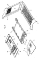
- the embodiment of the invention shown in Fig. 1 shows a as Combination chip card reader trained contacting unit 1, which is provided via a standard PCMCIA interface is contacted with a computer are:
- the contact unit 1 consists of a housing 2 with a base plate 3, a connector panel 4 on the in the direction of insertion according to the arrow front end, a slide guide 5 at the opposite end and a cover element extending parallel and at a distance from the base plate 3 6, which - like the base plate 3 - the connection panel 4 with the slide-in guide 5 rigidly connects.
- the base plate 3 and the cover element 6 are as one-piece sheet metal part formed according to FIG. 3.
- the cover element 6 consists - like the base plate 3 - of sheet metal and is closed a U-shaped cross section bent sideways to on both long sides of the Contact unit 1 to provide a side sheet metal cover 12, the PCB frame 27 or the PCMCIA circuit board 7 covers up to the lower longitudinal edge, in order to obtain a complete lateral housing surround of the printed circuit board 7.
- the side The area between the sheet metal covers 12 and the base plate 3 remains open, so that the chip card guide area is without cover and the Total width of the contact unit in the computer plug-in area only the standardized Width of the ISO chip card 9 corresponds.
- mounting and Contacting the chip card 9 inserted into the insertion channel 8 are at the insertion end, adjacent to the connector panel 4, corner side two stops 13 arranged in the insertion channel 8, their contact surfaces with the chip card 9 corresponding to its corner rounding or bevel are formed so that there is a centering guidance of the chip card movement in the desired end position when inserting.
- the shape in Fig. 1 by an enlarged circular section drawing is clarified.
- the base plate 3 is at the insertion slot 10 of the insertion guide 5, approximately Stops 13 opposite each other with slightly protruding clamping cams 14 made of metal or plastic, with which the inserted chip card is set in the insertion channel 8 to prevent it from slipping out unintentionally to prevent.
- the chip card 9 is thus locked in the transverse and longitudinal directions. For better insertion of the chip card, there are run-in slopes on the clamping cams and / or the insertion slot. For easier removal the inserted and fixed according to the description above chip card 9 in the cover element 6 and / or in the base plate 3 central part-circular recesses 15 provided the user with convenient access to the card enable.
- Complementary are the opposite of the clamping cams Areas of the cover element 6 set back in a partially circular shape at 16 in order to To facilitate insertion and locking of the chip card 9.
- the Evaluation of an additional mini chip card 17 enables by on the PCMCIA circuit board 7, an electrical contact element 18 is arranged, the provides a connection to the integrated circuit of the PCMCIA card and by the correspondingly arranged chip field 19 of the mini chip card 17 can be contacted.
- the contact element 18 arranged cassette holder 20 which can be folded out of the cover element, under which the cover element is cut out accordingly.
- Fig.1 the shown folded up position, the introduction of the mini-chip card 17th allows. After inserting it into the cassette compartment, it is placed on the level of the cover element 6 is folded and thus the contacting of the chip field 19 with the PCMCIA card via the contact element 18.
- the contact element 18 can be used as a plug or as a rubber strip 21 according to Figure 2 of the drawing.
- a contact unit is the cassette part through a longitudinal web 22 divided into two compartments, in the two correspondingly small Mini chip memory cards can be inserted through the conductive rubber 21st can be contacted on the left and through the plug part 23 on the right.
Landscapes
- Engineering & Computer Science (AREA)
- Physics & Mathematics (AREA)
- General Physics & Mathematics (AREA)
- Theoretical Computer Science (AREA)
- Artificial Intelligence (AREA)
- Computer Vision & Pattern Recognition (AREA)
- Computer Hardware Design (AREA)
- Microelectronics & Electronic Packaging (AREA)
- Coupling Device And Connection With Printed Circuit (AREA)
- Credit Cards Or The Like (AREA)
- Details Of Connecting Devices For Male And Female Coupling (AREA)
Description
Die Erfindung betrifft eine Kontaktiereinheit für ein kartenförmiges Trägerelement elektronischer Baugruppen, insbesondere eine PCMCIA- Karte, mit den Merkmalen des Oberbegriffs des Anspruchs 1. Eine derartige Kontaktiereinheit ist beispielsweise aus der EP 0 704 813 A2 bekannt. The invention relates to a contacting unit for a card-shaped carrier element of electronic assemblies, in particular a PCMCIA card, with the features of the preamble of claim 1. Such a contacting unit is known, for example, from EP 0 704 813 A2.
Im Bereich der Computertechnologie werden elektronische Baugruppen vorzugsweise auf kartenförmigen Trägerelementen angeordnet Diese weisen Kontaktbereiche auf und sind in Kontaktiereinheiten einschiebbar, wo sie elektrisch kontaktiert und in den Datenkreislauf integriert werden. Hierzu gehören die sogenannten Chip-Karten, die derzeit beispielsweise als Telefonkarten Verwendung finden. Sie weisen flächig angeordnete Kontaktfelder für die Kontaktierung eines Chips auf und werden in als Leseeinheiten ausgebildete Kontaktiereinheiten eingeschoben.In the field of computer technology, electronic assemblies are used preferably arranged on card-shaped support elements Contact areas open and can be inserted into contact units where they are electrical contacted and integrated into the data cycle. These include the So-called chip cards, which are currently used, for example, as telephone cards Find use. They have flat contact fields for the Contacting a chip and are designed as reading units Contact units inserted.
Ferner sind beispielsweise aus der DE 295 05 678 U1 oder der DE 296 02 632 U1 kartenförmige Trägerelemente nach PCMCIA-Norm bekannt, die ein genormtes matrixartiges, an ihrer vorderen Einsteckkante ausgebildetes, steckbares Anschlußkontaktfeld aufweisen und unterschiedlichste IC-Schaltkreise aufnehmen können. Derartige Karten können Speichererweiterungskarten, Laufwerkskarten, Modemkarten u. dgl. sein. Sie lassen sich in Kontaktiereinheiten mit einer entsprechenden Stiftmatrix kontaktieren, wozu sie in den Einschubschlitz, beispielsweise eines Computers eingeschoben werden. Furthermore, for example from DE 295 05 678 U1 or DE 296 02 632 U1 card-shaped carrier elements according to the PCMCIA standard are known which have a standardized matrix-like, plug-in connection contact field formed on their front insertion edge and can accommodate a wide variety of IC circuits. Such cards can memory expansion cards, drive cards, modem cards and. the like. They can be contacted in contacting units with a corresponding pin matrix, for which purpose they are inserted into the insertion slot, for example of a computer.
Aus der EP 0552 078 A1 ist ferner die Kombination dieser bekannten Kartensysteme bekannt, wodurch gleichzeitig eine PCMCIA-Karte und eine Chip-Karte in einen entsprechenden Modulaufnahmeschlitz eines Computers eingeschoben und gelesen werden können. Nachteilig sind hier das Freiliegen des Kontaktfeldes und die mangelhafte Führung der Chip-Karte, die darüber hinaus auch in ihrer Betriebsposition relativ zur PCMCIA-Karte bewegbar ist, so daß eine sichere Kontaktierung nicht gewährleistet ist.The combination of these is also known from EP 0552 078 A1 Card systems known, whereby a PCMCIA card and a chip card simultaneously into a corresponding module slot in a computer can be inserted and read. Disadvantages are the exposure of the Contact field and the poor management of the chip card beyond that is also movable in its operating position relative to the PCMCIA card, so that a secure contacting is not guaranteed.
Eine besondere Ausbildung der Chipkartenaufnahme und Möglichkeit zum einfachen Anschluß an den Computer wird hierzu in der DE 43 10 517 A1 vorgeschlagen, indem an der Kontaktiereinheit der PCMCIA-Karte ein Einschubkanal für die Chip-Karte und eine Einschubführung ausgebildet sind, die einen gegenüber der PCMCIA-Karte vorstehenden Bereich aufweist, der ein sicheres Einstecken der gesamten Kontaktiereinheit in den Modulaufnahmeschlitz des Computers ermöglicht. Nachteiligerweise weicht dieser Vorschlag jedoch stark von der normierten Ausgestaltung der PCMCIA-Karte ab und kann ebenfalls nicht sicherstellen, daß die Chip-Karte in ihrer Kontaktierungsposition unverschiebbar ist. Ein sicherer Betrieb im Sinne einer Vielfachbetätigung an Automaten und dgl. kann mit den vorbekannten Kontaktiereinheiten nicht gewährleistet werden. Darüber hinaus ist durch die an den Längsseiten völlig offene Konstruktion des Gehäuses die mechanische Stabilität der Kontaktiereinheit und deren Torsionssteifigkeit gering, so daß die Funktionssicherheit im Langzeitbetrieb gefährdet ist.Special training in chip card recording and the possibility of simple connection to the computer is in DE 43 10 517 A1 proposed by adding a contact to the PCMCIA card Insertion channel for the chip card and an insertion guide are formed has an area protruding from the PCMCIA card, which is a secure insertion of the entire contact unit into the module slot of the computer. Unfortunately, this proposal gives way strongly on the standardized design of the PCMCIA card and also cannot ensure that the chip card is immovable in its contacting position is. Safe operation in the sense of multiple operation on machines and the like. cannot be guaranteed with the known contacting units. In addition, the completely open construction on the long sides of the Housing the mechanical stability of the contact unit and its torsional rigidity low, so that the functional safety in long-term operation is at risk.
Ausgehend von diesem Stand der Technik liegt der Erfindung die Aufgabe zugrunde, eine Kontaktiereinheit der eingangs genannten Art unter Meidung der beschriebenen Nachteile dadurch zu verbessern, daß eine sichere Halterung, Kontaktierung und Führung in der Kombination einer PCMCIA-Karte mit einer oder mehreren zusätzlich einschiebbaren Chip-Karten gewährleistet ist und das Gehäuse der Kontaktiereinheit bei kleinsten Abmessungen eine hohe Torsionssteifigkeit, Festigkeit und damit Dauerhaltbarkeit aufweist.Based on this prior art, the invention has for its object to improve a contacting unit of the type mentioned while avoiding the disadvantages described in that a secure mounting, contacting and guidance in the combination of a PCMCIA card with one or more additional insertable chip -Cards is guaranteed and the housing of the contact unit with the smallest dimensions has high torsional rigidity, strength and thus durability.
Die Aufgabe ist bei einer Kontaktiereinheit mit den Merkmalen des Oberbegriffs des Anspruchs 1 erfindungsgemäß durch die Merkmale des kennzeichnenden Teils des Anspruchs 1 gelöst. The object is achieved in a contacting unit with the features of the preamble of claim 1 according to the invention by the features of the characterizing part of claim 1 .
Hierdurch wird die Stabilität der Kontaktiereinheit in ihrer Gesamtheit deutlich erhöht und, eine sichere Positionierung der eingeschobenen Chip-Karte in ihrer Kontaktierungsposition erreicht und der Anwendungsbereich der erfindungsgemäßen Kontaktiereinheit erweitert, wozu sie aufgrund Ihrer Stabilität und Kompaktheit geeignet ist. As a result, the stability of the contacting unit as a whole is significantly increased and, a secure positioning of the inserted chip card in its contacting position is achieved and the area of application of the contacting unit according to the invention is expanded, for which it is suitable due to its stability and compactness.
Eine weitere Verbesserung kann gemäß einer zweckmäßigen Ausgestaltung der Erfindung dadurch herbeigeführt werden, daß an der Einschubführung für die Chip-Karte eine Verriegelungeinrichtung, vorzugsweise in Form zweier mit den Anschlägen korrespondierender Klemmnocken, vorgesehen wird, mit der die Chip-Karte in ihrer Endposition - bei Bedarf wieder entnehmbar - gesichert wird.A further improvement can be according to an expedient embodiment of the Invention can be brought about in that on the insertion guide for the chip card a locking device, preferably in the form of two with the Stops corresponding clamp cams are provided with which the chip card is secured in its end position - removable if necessary.
Vorzugsweise besteht die Kontaktiereinheit aus einem Gehäuse mit einem die Leiterplatte der PCMCIA-Karte haltenden Rahmen, an dessen einer Stirnseite die Einschubführung und an dessen anderer Stirnseite das Anschlußfeld angeordnet sind, die durch die mit Abstand parallel zur Leiterplatte verlaufende Basisplatte miteinander verbunden sind derart, daß ein Einschubkanal für die Chip-Karte gebildet ist, der endseitig durch die beiden Anschläge und Klemmnocken begrenzt ist, wobei die seitlichen Abdeckungen zwischen Einschubführung und Anschlußfeld den Rahmen bis zur Dicke der Leiterplatte bedecken und den Einschubkanal seitlich freilassen. Vorteilhafterweise sind die seitlichen Abdeckungen an einem den Rahmen an der Oberseite abschließenden Deckelelement, insbesondere aus Blech, durch leistenförmige Abbiegungen zur U-Querschnittsform ausgebildet, um die Gehäusefestigkeit weiter zu erhöhen.The contacting unit preferably consists of a housing with a die Circuit board of the PCMCIA card holding frame, on one end of which the Slide-in guide and the other side of the connector panel are by the base plate running parallel to the circuit board at a distance are interconnected such that an insertion channel for the chip card is formed, which is limited at the end by the two stops and clamping cams is, the side covers between the slide-in guide and the connector panel cover the frame to the thickness of the circuit board and the insertion channel leave at the side. The side covers are advantageously on one the frame at the top closing cover element, in particular Sheet metal, formed by strip-shaped bends to form a U cross-section to further increase the housing strength.
Diesem Ziel dient auch der weitere Vorschlag der Erfindung, den Rahmen als einstückiges Kunststoffteil auszubilden und mit der Basisplatte und dem Deckelelement zu einer Einheit zu verbinden, wobei die Basisplatte und das Deckelelement als einstückiges Blechteil ausgebildet sind. Die Einschubführung kann in zweckmäßiger Ausgestaltung der Erfindung mit Einlaufschrägen ausgestattet sein und es kann der den Klemmnocken gegenüberliegende Bereich mit einer Ausnehmung zurückspringend ausgebildet sein, um die Einführung, Entarretierung und Entnahme der Chip-Karte zu vereinfachen. Das elektrische Kontaktelement ist vorzugsweise ein Leitgummistreifen. Die Mini-Chip-Kartenaufnahme kann z.B. durch einen oder mehrere Stege in Fächer zur Aufnahme mehrerer Mini-Chip-Karten unterteilt sein, so daß ein Kombichipkartenlesegerät geschaffen ist, das eine PCMCIA-Karte mit einer Chip-Karte nach DIN/ISO 7816 und einer oder mehreren Mini-Chip-Karten kombiniert. Eine derartige Kontaktiereinheit nach der Erfindung erlaubt das Einbringen der Chip- und Mini-Chip-Karten ohne verbreiterten Kartenführungsbereich auch bei einem Lesesystem der PCMCIA-Norm entsprechenden Kartentypen I, II oder III. Dabei kann ergänzend in der Basisplatte ein Fenster in der Größe des Chip-Kartenlesers eingebracht sein, um mit einem fremden Kartensystem eine Personalisierung des Moduls vornehmen zu können, z.B. für das Nachladen des Lesers für zusätzliche Daten oder Veränderungen.The further proposal of the invention, the frame as form one-piece plastic part and with the base plate and To connect the cover element to a unit, the base plate and the Cover element are formed as a one-piece sheet metal part. The slide-in guide can in an expedient embodiment of the invention with chamfers be equipped and it can be the area opposite the clamping cams be recessed with a recess to facilitate the introduction, Simplify unlocking and removal of the chip card. The electrical contact element is preferred a conductive rubber strip. The mini chip card holder can e.g. by one or several webs divided into compartments to hold several mini-chip cards be so that a combination chip card reader is created that a PCMCIA card with a chip card according to DIN / ISO 7816 and one or more mini chip cards combined. Such a contacting unit according to the invention allows the insertion of the chip and mini-chip cards without a widened card guiding area even with a reading system that complies with the PCMCIA standard Card types I, II or III. A window can also be added to the base plate the size of the chip card reader to be brought in with someone else Card system to be able to personalize the module, e.g. For reloading the reader for additional data or changes.
Zweckmäßigerweise ist die Mini-Chip-Kartenaufnahme als Kassettenmechanismus mit einer Rast/Entrasteinrichtung versehen, vorzugsweise in einer Anordnung, die eine Entriegelung im gesteckten Betriebszustand der Kontaktiereinheit nicht ermöglicht, wobei über die schrägstehende Kassettenlage in Öffungsstellung während des Schließvorgangs eine Kontaktselbstreinigung dadurch vorgenommen wird, daß eine Kontaktflächenreibung zwischen Chip und elektrischem Kontaktelement bewirkt wird. Durch die im Nutzungszustand geschlossene Kassette werden die Kontaktelemente darüber hinaus gegen Verschmutzungen und Zugriff geschützt. Dazu kann es vorteilhaft sein, in der Mini-Chip-Kartenaufnahme Andruck- oder Haltefedern vorzusehen, mit denen die eingesetzte Karte in Kontaktfunktionslage gebracht wird. Zusätzlich können seitliche Andruckfedern vorgesehen sein, die die eingesetzte Karte seitlich klemmen und dadurch Schutz gegen Herausfallen bei geöffneter Kassette bieten.The mini-chip card holder is expediently used as a cassette mechanism provided with a locking / unlocking device, preferably in one Arrangement that unlocks the inserted operating state of the contact unit not possible, with the inclined cassette in Opening position during the closing process a contact self-cleaning is made that a contact surface friction between the chip and electrical contact element is effected. By the closed in the state of use Cassette will also be the contact elements against contamination and access protected. It can be advantageous to do this in the mini-chip card holder Provide pressure or retaining springs with which the inserted card is brought into contact function position. In addition, lateral Pressure springs are provided which laterally clamp the card inserted and thus offer protection against falling out when the cassette is open.
Weitere Einzelheiten, Vorteile und Merkmale der Erfindung ergeben sich aus der nachfolgenden Beschreibung der zugehörigen Zeichnung, in der zwei bevorzugte Ausführungsformen eines erfindungsgemäßen Kombichipkartenlesers schematisch dargestellt sind. In der Zeichnung zeigt:
- Fig. 1
- eine Kontaktiereinheit perspektivisch mit in Einsteckvorbereitung befindlichen Chip-Karten;
- Fig. 2
- eine modifizierte Kontaktiereinheit und
- Fig. 3
- eine Explosionsdarstellung der Kontaktiereinheit der Fig. 2 perspektivisch.
- Fig. 1
- a contacting unit in perspective with chip cards in preparation for insertion;
- Fig. 2
- a modified contact unit and
- Fig. 3
- an exploded view of the contact unit of FIG. 2 in perspective.
Das in Fig. 1 dargestellte Ausführungsbeispiel der Erfindung zeigt eine als
Kombichipkartenleser ausgebildete Kontaktiereinheit 1, die vorgesehen ist, über
eine normgemäße PCMCIA-Schnittstelle mit einem Computer kontaktiert zu
werden: Die Kontaktiereinheit 1 besteht aus einem Gehäuse 2 mit einer Basisplatte
3, einem Anschlußfeld 4 an dem in Einschubrichtung gemäß Pfeil
vorderen Ende, einer Einschubführung 5 am gegenüberliegenden Ende und
einem parallel mit Abstand zur Basisplatte 3 sich erstreckenden Deckelelement
6, welches - wie die Basisplatte 3 - das Anschlußfeld 4 mit der Einschubführung
5 starr verbindet. Die Basisplatte 3 und das Deckelelement 6 sind als
einstückiges Blechteil entsprechend Fig. 3 ausgebildet. Dabei werden die
genannten Elemente von einem innenliegenden Rahmen 27 aus PCB getragen
(siehe Fig. 3), der eine PCMCIA-Leiterplatte 7 mit Abstand parallel zur
Basisplatte 3 derart hält, daß dazwischen ein Einschubkanal 8 für eine ISO 7816
Chip-Karte 9 gebildet wird, die über einen Einschubschlitz 10 der
Einschubführung 5 in die Kontaktiereinheit 1 einschiebbar ist. Die Chip-Karte 9
läßt sich in Richtung des gezeigten Doppelpfeils in die Kontaktiereinheit 1
einschieben und aus dieser wieder herausziehen, wobei über das auf die
Oberfläche angeordnete Chipfeld 11 der Chip-Karte 9 und Kontaktelemente 11'
auf der Unterseite der PCMCIA-Leiterplatte 7 eine Kontaktierung vornehmbar ist,
die eine Verarbeitung der Chip-Karte über die PCMCIA-Karte ermöglichen, wenn
die letztgenannte in den Einschubschlitz eines elektronischen
Verarbeitungsgerätes eingesetzt ist und mit dessen PCMCIA-Schnittstelle über
das Anschlußfeld 4 verbunden ist:The embodiment of the invention shown in Fig. 1 shows a as
Combination chip card reader trained contacting unit 1, which is provided via
a standard PCMCIA interface is contacted with a computer
are: The contact unit 1 consists of a
Das Deckelelement 6 besteht - wie die Basisplatte 3 - aus Blech und ist zu
einem U-förmigen Querschnitt seitlich abgebogen, um an beiden Längsseiten der
Kontaktiereinheit 1 eine seitliche Blechabdeckung 12 bereitzustellen, die den
PCB-Rahmen 27 bzw. die PCMCIA-Leiterplatte 7 bis zur unteren Längskante abdeckt,
um eine komplette seitliche Gehäuseeinfassung der Leiterplatte 7 zu erhalten.
Dabei ist das Deckelelement 6 und sind ggfs. die Blechabdeckungen 12
mit der Einschubführung 5 sowie dem Anschlußfeld 4 fest, insbesondere durch
Verschweißen, verbunden, um ein insgesamt torsionssteifes durch den
eingesetzten Rahmen 27 stabilisiertes Gehäuse 2 auszubilden. Der seitliche
Bereich zwischen den Blechabdeckungen 12 und der Basisplatte 3 bleibt offen,
so daß der Chip-Kartenführungsbereich ohne Abdeckung ist und die
Gesamtbreite der Kontaktiereinheit im Computersteckbereich nur der genormten
Breite der ISO-Chip-Karte 9 entspricht. Um trotz des seitlich offenen Chip-Kartenführungsbereichs
eine sichere Positionierung, Halterung und
Kontaktierung der in den Einschubkanal 8 eingeschobenen Chip-Karte 9 zu erreichen,
sind am Einsteckende, dem Anschlußfeld 4 benachbart, eckenseitig
zwei Anschläge 13 im Einschubkanal 8 angeordnet, deren Berührungsflächen
mit der Chip-Karte 9 korrespondierend zu deren Eckrundung oder -schräge
ausgebildet sind, so daß sich eine zentrierende Führung der Chip-Kartenbewegung
in die gewünschte Endposition beim Einschieben ergibt. Damit
ist sowohl das Einstecken der Chip-Karte in den Einschubkanal 8 durch die
Einschubführung 5 als auch die Endpositionierung durch die Anschläge 13
geführt, deren Form in Fig. 1 durch eine vergrößerte Kreisausschnittszeichnung
näher verdeutlicht ist.The
Die Basisplatte 3 ist am Einschubschlitz 10 der Einschubführung 5, etwa den
Anschlägen 13 gegenüberliegend mit geringfügig hochstehenden Klemmnocken
14 aus Metall oder Kunststoff versehen, mit denen die eingeschobene Chip-Karte
im Einschubkanal 8 festgesetzt wird, um ein ungewolltes Herausrutschen
zu verhindern. Die Chip-Karte 9 ist somit in Quer- und Längsrichtung arretiert.
Zur besseren Einführung der Chip-Karte können Einlaufschrägen an den Klemmnocken
und/oder dem Einschubschlitz ausgebildet sein. Zur leichteren Entnahme
der eingeschobenen und gemäß obiger Beschreibung fixierten Chip-Karte 9 sind
im Deckelelement 6 und/oder in der Basisplatte 3 mittige teilkreisförmige Aussparungen
15 vorgesehen, die dem Benutzer einen günstigen Zugriff zur Karte
ermöglichen. Ergänzend sind die den Klemmnocken gegenüberliegenden
Bereiche des Deckelelements 6 teilkreisförmig bei 16 zurückgesetzt, um die
Einführung und Verriegelung der Chip-Karte 9 zu erleichtern.The
Mit der als Kombichipkartenleser ausgebildeten Kontaktiereinheit 1 ist ferner die
Auswertung einer zusätzlichen Mini-Chip-Karte 17 ermöglicht, indem auf der
PCMCIA-Leiterplatte 7 ein elektrisches Kontaktelement 18 angeordnet ist, das
einen Anschluß an den integrierten Schaltkreis der PCMCIA-Karte bereitstellt
und durch das korrespondierend angeordnete Chipfeld 19 der Mini-Chip-Karte
17 kontaktierbar ist. Zu deren Halterung ist über, dem Kontaktelement 18 eine
aus dem Deckelelement herausklappbare Kassettenaufnahme 20 angeordnet,
unter der das Deckelelement entsprechend ausgeschnitten ist. In Fig.1 ist die
hochgeklappte Stellung dargestellt, die die Einführung der Mini-Chip-Karte 17
ermöglicht. Nach deren Einschub in das Kassettenfach wird dieses in die Ebene
des Deckelelements 6 eingeklappt und wird damit die Kontaktierung des Chipfeldes
19 mit über das Kontaktelement 18 mit der PCMCIA-Karte vorgenommen.
Dazu kann das Kontaktelement 18 als Stecker oder auch als Leitgummistreifen
21 gemäß Fig.2 der Zeichnung ausgebildet sein. Bei dem dort dargestellte Ausführungsbeispiel
einer Kontaktiereinheit ist der Kassettenteil durch einen Längssteg
22 in zwei Fächer unterteilt, in die zwei entsprechend klein ausgebildete
Minichip-Speicherkarten eingesetzt werden können, die durch das Leitgummi 21
links und durch den Steckerteil 23 rechts kontaktierbar sind.With the contacting unit 1 designed as a combination chip card reader, the
Evaluation of an additional
Die Kassettenaufnahme der Fig. 2 weist einen auf das Deckelelement 6 aufgesetzten
Kassettenrahmen 24 mit Gelenkteil für den Klappmechanismus und vorn
angebrachtem Rast- und Entrastmechanismus 25 auf. Aufgrund der schrägen
Kassettenlage beim Beladen mit bestimmtem Anstellwinkel findet beim Schließen
eine Kontaktselbstreinigung statt, da die beiderseitigen Kontaktflächen während
der Schließbewegung der Kassette aneinanderreiben mit einer sich in der
Positionierung verändernden Reibkante. Durch die im Benutzungszustand völlig
geschlossene Kassette sind die Kontaktelemente vor Zugriff und Verschmutzung
geschützt.2 has one placed on the
Im Kassettenrahmen sind neben dem Rastmechanismus 25 Andruck- und Haltefedern
26 angeordnet, durch die die eingeschobenen Chip-Karten in die Kontaktfunktionslage
gebracht werden. Zusätzlich können sich in der
Kassettenaufnahme 20 seitlich Andruckfedern befinden, die die Karten seitlich
einklemmen und Schutz gegen Herausfallen bei geöffnetem Zustand der.
Kassette bieten. In addition to the locking mechanism, there are 25 pressure and retaining springs in the
- 11
- Kontaktiereinheitcontacting
- 22
- Gehäusecasing
- 33
- Basisplattebaseplate
- 44
- Anschlußfeldconnection panel
- 55
- Einschubführunginsertion guide
- 66
- Deckelelementcover element
- 77
- PCMCIA-LeiterplattePCMCIA board
- 88th
- Einschubkanalinsertion channel
- 99
- Chip-KarteSmart card
- 1010
- Einschubschlitzslot
- 1111
- Chipfeldchip box
- 11'11 '
- Kontaktelementecontact elements
- 1212
- Blechabdeckungmetal cover
- 1313
- Anschlägeattacks
- 1414
- Klemmnockenclamping cams
- 1515
- Aussparungen, AusnehmungRecesses, recess
- 1616
- Teilkreis-AusnehmungenPartial circle recesses
- 1717
- Mini-Chip-KarteMini chip card
- 1818
- Kontaktelementcontact element
- 1919
- Chipfeldchip box
- 2020
- Kassettenaufnahmecassette holder
- 2121
- LeitgummistreifenLeitgummistreifen
- 2222
- Längssteglongitudinal web
- 2323
- Steckerteilplug part
- 2424
- Kassettenrahmencassette frame
- 2525
- Rast-/EntrastmechanismusLatching / Entrastmechanismus
- 2626
- Andruck- und HaltefedernPressure and holding springs
- 2727
- Rahmenframe
Claims (13)
- Contacting unit for a card-shaped carrier element for electronic modules, in particular in accordance with the PCMCIA Standard, with a housing (2) having a slot-shaped insertion channel (8) for the card-shaped carrier element, in particular a chip card (9), in which a circuit board (7) is disposed which, in addition to a connecting field (4) arranged at one edge is provided on one surface with contact elements (11') for contacting the card-shaped carrier element (9), where the card-shaped carrier element (9) may be inserted in parallel with the circuit board (7) into the slot shaped insertion channel (8) of housing (2) of the contacting unit (1) that is formed between a base plate (3) of the housing (2) and the circuit board (7) so as to be open on its side and has an insertion guide (5) for the card-shaped carrier element (9) at its end which is opposite to the connecting field (4), and where two end stops (13) that limit the depth of insertion of the card-shaped carrier element (9) at the comers are provided at the connecting field (4), where the end stops have a sloping contour matching the comer shape of the card-shaped carrier element (9), or a radiused contour that matches the shape of the comer of the card-shaped carrier element (9),
characterised in that the insertion guide (5) for the card-shaped carrier element (9) is extended beyond the insertion area in the form of a side cover (12) into the area of the connecting field (4) and that the circuit board (7) has at least one further electrical contacting element (18), in particular a plug (23), by means of which a mini chip card holder (20) of the contacting unit (1) that can be folded out from the surface of the contacting unit (1) may be electronically contacted, where insertion and removal of a mini chip card (17) can be effected with the mini chip card holder (20) folded out, whereas in the closed state of the mini chip card holder (20) electrical contacting of the mini chip card (17) inserted into the mini chip card holder (20), in particular for the reading function, is effected. - Contacting unit in accordance with Claim 1, characterised in that a latching mechanism, preferably in the form of two locating cams (14) corresponding to the end stops (13), is provided at the insertion guide (5) for the card-shaped carrier element (9), with which the card-shaped carrier element (9) can be latched - removably, if required - in its final position.
- Contacting unit in accordance with Claim 1 or 2, characterised in that the contacting unit (1) consists of a housing (2) with a frame (27) holding the circuit board (7), where the insertion guide (5) is provided at one facing end of the housing, and the connecting field (4) at the opposite facing end of the housing and these are connected by means of a base plate (3) extending at a distance from, and in parallel with, the circuit board (7) in such a manner that the insertion channel (8) for the card-shaped carrier element (9) is formed which is limited at the end by the two end stops (13) and locating cams (14), where the side covers (12) between the insertion guide (5) and the connecting field (4) cover the frame (27) up to the thickness of the circuit board (7) and leave the insertion channel (8) open on its side.
- Contacting unit in accordance with Claim 3, characterised in that the frame (27) is designed as a one-piece plastics part and is made into a single unit with the base plate (3) and one cover element (6) of housing (2), where the base plate (3) and the cover element (6) are formed as a one-piece sheet metal part.
- Contacting unit in accordance with Claim 3 or Claim 4, characterised in that the side covers (12) are formed into U-shaped channels from a cover element (6) made in particular of sheet metal that finishes the top of the frame (27).
- Contacting unit in accordance with one of Claims 1 to 5, characterised in that the insertion guide (5) has sloping insert portions.
- Contacting unit in accordance with one of Claims 2 to 6, characterised in that the area opposite to the locating cams (14) is formed with a cut out recess (15).
- Contacting unit in accordance with one of Claims 1 to 7, characterised in that the electrical contacting element (18) is a conductive rubber strip (21).
- Contacting unit in accordance with one of Claims 1 to 8, characterised in that the mini chip card holder (20) is subdivided by one or several webs (22) into compartments for the accommodation of several mini chip cards (17) so that a combined chip card reader in accordance with the PCMCIA standard is obtained which combines a card-shaped carrier element (9) in accordance with DIN/ISO 7816, and in particular a chip card (9) and one or several mini chip cards (17).
- Contacting unit in accordance with one of Claims 1 to 9, characterised in that there is a window of the size of the chip card reader in the base plate (3) of the housing (2) so as to be able to personalise the module in an alien card system.
- Contacting unit in accordance with one of Claims 1 to 10, characterised in that the mini chip card holder (20), as a cassette mechanism, is provided with a latching/releasing mechanism (25), preferably in an arrangement which does not allow release in inserted operating condition of the contacting unit (1) where, owing to the sloping cassette position in the open position, self-cleaning of the contacts is achieved, due to friction between the contact faces of the chip field (19) of a mini chip card (17) and the electrical contacting element (18).
- Contacting element in accordance with one of Claims 1 to 11, characterised in that compression or retaining springs (26) are provided in the mini chip card holder (20) with which a mini chip card (17) inserted into the mini chip card holder (20) can be brought into the functional contact position.
- Contacting unit in accordance with one of claims 1 to 12, characterised in that lateral compression springs are provided which clamp a mini chip card (17) inserted into the mini chip card holder (20) laterally and hence protect it from falling out when the mini chip card holder (20) is open.
Priority Applications (1)
| Application Number | Priority Date | Filing Date | Title |
|---|---|---|---|
| EP03027001A EP1418528B1 (en) | 1996-04-22 | 1997-04-05 | Chip card reader |
Applications Claiming Priority (2)
| Application Number | Priority Date | Filing Date | Title |
|---|---|---|---|
| DE29607253U | 1996-04-22 | ||
| DE29607253U DE29607253U1 (en) | 1996-04-22 | 1996-04-22 | Combi chip card reader |
Related Child Applications (1)
| Application Number | Title | Priority Date | Filing Date |
|---|---|---|---|
| EP03027001A Division EP1418528B1 (en) | 1996-04-22 | 1997-04-05 | Chip card reader |
Publications (3)
| Publication Number | Publication Date |
|---|---|
| EP0803833A2 EP0803833A2 (en) | 1997-10-29 |
| EP0803833A3 EP0803833A3 (en) | 1998-08-05 |
| EP0803833B1 true EP0803833B1 (en) | 2003-11-26 |
Family
ID=8022915
Family Applications (2)
| Application Number | Title | Priority Date | Filing Date |
|---|---|---|---|
| EP97105660A Expired - Lifetime EP0803833B1 (en) | 1996-04-22 | 1997-04-05 | Combined chip card reader |
| EP03027001A Expired - Lifetime EP1418528B1 (en) | 1996-04-22 | 1997-04-05 | Chip card reader |
Family Applications After (1)
| Application Number | Title | Priority Date | Filing Date |
|---|---|---|---|
| EP03027001A Expired - Lifetime EP1418528B1 (en) | 1996-04-22 | 1997-04-05 | Chip card reader |
Country Status (5)
| Country | Link |
|---|---|
| US (1) | US5877488A (en) |
| EP (2) | EP0803833B1 (en) |
| JP (1) | JP3689528B2 (en) |
| DE (3) | DE29607253U1 (en) |
| SG (1) | SG54496A1 (en) |
Families Citing this family (97)
| Publication number | Priority date | Publication date | Assignee | Title |
|---|---|---|---|---|
| DE19629086A1 (en) | 1996-07-18 | 1998-01-29 | Siemens Ag | Portable data transmission device and fastener |
| DE19629351C2 (en) * | 1996-07-20 | 2002-10-24 | Wolfgang Neifer | Mobile chip card reading module |
| DE29617034U1 (en) | 1996-09-30 | 1996-12-05 | Stocko Metallwarenfabriken Henkels & Sohn GmbH & Co, 42327 Wuppertal | PC card adapter |
| JPH10302030A (en) * | 1997-02-28 | 1998-11-13 | Toshiba Corp | Connection device and information processing device |
| DE29704984U1 (en) * | 1997-03-19 | 1997-05-07 | Stocko Metallwarenfabriken Henkels & Sohn GmbH & Co, 42327 Wuppertal | Adapter for contacting card-shaped carrier elements |
| DE19716694A1 (en) * | 1997-04-21 | 1998-10-22 | Scm Microsystems Gmbh | Interface for IC card |
| EP0976082B1 (en) | 1997-04-18 | 2002-02-27 | SCM Microsystems GmbH | Interface device for chip cards |
| DE19716423C1 (en) * | 1997-04-18 | 1998-11-05 | Robert Schneider | Chip card reader e.g. for computer |
| DE19729397A1 (en) * | 1997-07-09 | 1998-11-05 | Siemens Ag | Reception arrangement for card-shaped data carrier |
| US6392881B1 (en) * | 1997-09-22 | 2002-05-21 | Citizen Watch Co., Ltd. | Portable electronic device |
| US6074616A (en) * | 1998-01-05 | 2000-06-13 | Biosite Diagnostics, Inc. | Media carrier for an assay device |
| US6392894B1 (en) | 1998-01-05 | 2002-05-21 | Biosite Incorporated | Media carrier for an assay device |
| US6015092A (en) * | 1998-02-05 | 2000-01-18 | Postlewaite; William M. | Smart card reader having angled smart card holder |
| DE59801853D1 (en) * | 1998-02-20 | 2001-11-29 | Stocko Contact Gmbh & Co Kg | Vertical, short chip card reader |
| DE29811425U1 (en) * | 1998-06-29 | 1998-09-17 | Stocko Metallwarenfabriken Henkels & Sohn GmbH & Co, 42327 Wuppertal | Contact unit for a card-shaped carrier element of electronic assemblies, in particular according to the PCMCIA standard |
| DE29812626U1 (en) | 1998-07-15 | 1998-11-12 | SCM Microsystems GmbH, 85276 Pfaffenhofen | Card readers for chip cards |
| KR20000009369A (en) | 1998-07-23 | 2000-02-15 | 윤종용 | Computer system capable of installation of pc card and booting method thereof |
| US6062887A (en) * | 1998-08-31 | 2000-05-16 | Motorola, Inc. | Electronic device with dual card reader employing a drawer |
| DE29817004U1 (en) | 1998-09-22 | 1999-01-28 | SCM Microsystems GmbH, 85276 Pfaffenhofen | Retrofittable interface device for a data processing device |
| US6240301B1 (en) * | 1998-10-29 | 2001-05-29 | Ericcson Inc. | Diversity antenna in a SIM card package |
| US6840801B1 (en) * | 1998-10-29 | 2005-01-11 | Steinbeck Cannery, Llc | Docking apparatus for PC card devices |
| EP1004979A1 (en) * | 1998-11-24 | 2000-05-31 | CANAL+ Société Anonyme | Portable electronic card |
| US6705529B1 (en) * | 1998-11-26 | 2004-03-16 | Nokia Mobile Phones, Ltd. | Data card holder and reader therefor |
| US6402032B1 (en) * | 1998-12-03 | 2002-06-11 | Integrated Technology Express Inc. | Integrated smart card reader and computer input/output IC system |
| DE29821644U1 (en) * | 1998-12-04 | 1999-02-18 | Stocko Metallwarenfab Henkels | Authentication system for PC cards |
| US6293464B1 (en) * | 1999-01-05 | 2001-09-25 | Jared Joseph Smalley, Jr. | Card reader |
| US7036738B1 (en) | 1999-05-03 | 2006-05-02 | Microsoft Corporation | PCMCIA-compliant smart card secured memory assembly for porting user profiles and documents |
| US7117369B1 (en) | 1999-05-03 | 2006-10-03 | Microsoft Corporation | Portable smart card secured memory system for porting user profiles and documents |
| DE29909222U1 (en) * | 1999-05-28 | 1999-08-05 | STOCKO Contact GmbH & Co. KG, 42327 Wuppertal | PC card chip card reader |
| DE19925146C2 (en) * | 1999-06-02 | 2003-01-09 | Itt Mfg Enterprises Inc | Plug-in card for electronic devices |
| US6315205B1 (en) | 1999-07-06 | 2001-11-13 | Itt Manufacturing Enterprises, Inc. | Adaptor for smart card |
| EP1073006A1 (en) * | 1999-07-26 | 2001-01-31 | Molex Incorporated | Chip card ejector system |
| US6213403B1 (en) * | 1999-09-10 | 2001-04-10 | Itt Manufacturing Enterprises, Inc. | IC card with fingerprint sensor |
| DE19947162C1 (en) * | 1999-10-01 | 2000-09-28 | Itt Mfg Enterprises Inc | Plug-in card for electronic equipment has frame element attached to housing part; chip card can be inserted into frame element to contacting device at end of frame element |
| US7487908B1 (en) * | 1999-10-23 | 2009-02-10 | Ultracard, Inc. | Article having an embedded accessible storage member, apparatus and method for using same |
| US8397998B1 (en) | 1999-10-23 | 2013-03-19 | Ultracard, Inc. | Data storage device, apparatus and method for using same |
| JP4053704B2 (en) * | 2000-01-05 | 2008-02-27 | 株式会社東芝 | IC card with built-in wireless interface function, antenna module, information processing device |
| CN1142669C (en) * | 2000-01-20 | 2004-03-17 | 国际商业机器公司 | Handheld device, smart card interface device and data transmission method |
| JP2001291070A (en) * | 2000-04-04 | 2001-10-19 | Jst Mfg Co Ltd | Connector device |
| US6824063B1 (en) * | 2000-08-04 | 2004-11-30 | Sandisk Corporation | Use of small electronic circuit cards with different interfaces in an electronic system |
| US7107378B1 (en) * | 2000-09-01 | 2006-09-12 | Sandisk Corporation | Cooperative interconnection and operation of a non-volatile memory card and an input-output card |
| AUPR008400A0 (en) * | 2000-09-12 | 2000-10-05 | Canon Kabushiki Kaisha | User configurable remote control |
| JP2002109484A (en) * | 2000-09-26 | 2002-04-12 | Toshiba Corp | Portable information devices |
| JP4671484B2 (en) * | 2000-10-11 | 2011-04-20 | ケル株式会社 | Card connector |
| CN1217450C (en) * | 2000-11-03 | 2005-08-31 | 安弗诺-图歇尔电子有限公司 | Intelligence card connector for connecting two intelligence cards |
| JP2002280097A (en) * | 2001-03-19 | 2002-09-27 | Jst Mfg Co Ltd | Flash memory card connector, connection structure using the same, and electronic device using the connection structure |
| US20020162884A1 (en) * | 2001-05-07 | 2002-11-07 | Speas Gary W. | Low-power smart-card module |
| DE20201237U1 (en) * | 2002-01-28 | 2002-06-13 | SCM Microsystems GmbH, 85737 Ismaning | Smart card reader |
| US7440774B2 (en) | 2002-04-08 | 2008-10-21 | Socket Mobile, Inc. | Wireless enabled memory module |
| US20030211763A1 (en) * | 2002-05-07 | 2003-11-13 | Roger Wu | Compact flash card having energizing device |
| DE20209185U1 (en) * | 2002-06-13 | 2003-10-23 | STOCKO Contact GmbH & Co. KG, 42327 Wuppertal | PC card chip card reader |
| US6786415B2 (en) * | 2002-08-06 | 2004-09-07 | Jung-Hua Yiu | Memory card connector |
| FR2845801B1 (en) * | 2002-10-14 | 2005-06-17 | Itt Mfg Enterprises Inc | ELECTRICAL CONNECTOR FOR THE SIMULTANEOUS CONNECTION OF TWO INTEGRATED CIRCUIT (S) CHARTS |
| EP1418527A1 (en) * | 2002-11-08 | 2004-05-12 | Motorola, Inc. | Multiple SIM card holding apparatus |
| US7367503B2 (en) * | 2002-11-13 | 2008-05-06 | Sandisk Corporation | Universal non-volatile memory card used with various different standard cards containing a memory controller |
| US20050055479A1 (en) * | 2002-11-21 | 2005-03-10 | Aviad Zer | Multi-module circuit card with inter-module direct memory access |
| US8037229B2 (en) * | 2002-11-21 | 2011-10-11 | Sandisk Technologies Inc. | Combination non-volatile memory and input-output card with direct memory access |
| USD492688S1 (en) | 2002-12-09 | 2004-07-06 | Sandisk Corporation | Memory card |
| JP4019965B2 (en) * | 2003-02-10 | 2007-12-12 | ソニー株式会社 | IC card adapter device |
| US6830194B2 (en) * | 2003-03-05 | 2004-12-14 | Wem Technology Inc. | Built-in multifunctional card reader |
| US6888724B2 (en) * | 2003-03-29 | 2005-05-03 | John Shaie | Network card device having protective structure |
| US7305535B2 (en) * | 2003-04-17 | 2007-12-04 | Sandisk Corporation | Memory cards including a standard security function |
| DE10350233A1 (en) * | 2003-10-27 | 2005-05-19 | Behr Gmbh & Co. Kg | Connector for joining consumer to bus system, for motor vehicle heating or air conditioning system, has flat cable contacting piece with electronic circuitry fixed in housing |
| US7209995B2 (en) * | 2003-12-09 | 2007-04-24 | Sandisk Corporation | Efficient connection between modules of removable electronic circuit cards |
| US8177129B2 (en) * | 2004-02-17 | 2012-05-15 | Timothy D. Larin | Interactive multimedia smart affinity card with flash memory |
| US7177159B2 (en) * | 2004-05-03 | 2007-02-13 | 3 View Technology Co., Ltd. | Packaging structure of electronic card |
| US6942153B1 (en) * | 2004-05-25 | 2005-09-13 | Unitech Electronics Co.,Inc. | Handheld computer |
| HK1063994A2 (en) * | 2004-06-09 | 2004-12-17 | 龙杰智能卡有限公司 | Smart card reader with contactless access capability |
| USD529029S1 (en) * | 2004-06-11 | 2006-09-26 | J.S.T. Mfg. Co., Ltd. | Memory card adapter |
| JP4707339B2 (en) * | 2004-07-12 | 2011-06-22 | 京セラ株式会社 | PC card |
| JP4698185B2 (en) * | 2004-09-02 | 2011-06-08 | 京セラ株式会社 | Information equipment card |
| TWI316713B (en) * | 2004-09-10 | 2009-11-01 | Murata Manufacturing Co | Card-type device |
| DE102005061688A1 (en) * | 2005-12-21 | 2007-07-05 | Stocko Contact Gmbh & Co. Kg | contacting |
| EP1873680A1 (en) * | 2006-06-23 | 2008-01-02 | ddm hopt + schuler GmbH & Co. KG. | Tamper proof card reader |
| SG148876A1 (en) * | 2007-06-08 | 2009-01-29 | Jst Mfg Co Ltd | Card connector |
| SG148874A1 (en) * | 2007-06-08 | 2009-01-29 | Mea Technologies Pte Ltd | Card connector |
| US7572152B2 (en) * | 2007-06-27 | 2009-08-11 | Sandisk Il Ltd. | Memory interface card with SIM functions |
| USD615983S1 (en) | 2007-12-06 | 2010-05-18 | Sony Corporation | Adapter for memory card |
| USD616429S1 (en) * | 2008-03-31 | 2010-05-25 | Nokia Corporation | Tray for a handset |
| US7713091B2 (en) * | 2008-09-12 | 2010-05-11 | Getac Technology Corp. | Adaptor device for connecting and accessing data card and computer device incorporating the adaptor device |
| USD642578S1 (en) * | 2009-09-30 | 2011-08-02 | Sony Corporation | Memory card adapter |
| US8152545B1 (en) * | 2011-07-19 | 2012-04-10 | Cheng Uei Precision Industry Co., Ltd. | Card connector |
| CN103311721B (en) * | 2012-03-16 | 2015-10-21 | 莫仕连接器(成都)有限公司 | Double SIM card pallet, connector modules and electric connector |
| USD707682S1 (en) * | 2012-12-05 | 2014-06-24 | Logomotion, S.R.O. | Memory card |
| USD759022S1 (en) | 2013-03-13 | 2016-06-14 | Nagrastar Llc | Smart card interface |
| USD758372S1 (en) | 2013-03-13 | 2016-06-07 | Nagrastar Llc | Smart card interface |
| US9647997B2 (en) | 2013-03-13 | 2017-05-09 | Nagrastar, Llc | USB interface for performing transport I/O |
| USD729808S1 (en) * | 2013-03-13 | 2015-05-19 | Nagrastar Llc | Smart card interface |
| US9888283B2 (en) | 2013-03-13 | 2018-02-06 | Nagrastar Llc | Systems and methods for performing transport I/O |
| WO2016086331A1 (en) * | 2014-12-04 | 2016-06-09 | 璩泽明 | Chip card, as well as carrier plate for carrying same, and method for forming same |
| USD780763S1 (en) | 2015-03-20 | 2017-03-07 | Nagrastar Llc | Smart card interface |
| USD864968S1 (en) | 2015-04-30 | 2019-10-29 | Echostar Technologies L.L.C. | Smart card interface |
| CN105768385A (en) * | 2016-02-25 | 2016-07-20 | 广东康城物业管理服务有限公司 | A portable key chain owner card |
| US9887476B2 (en) * | 2016-05-03 | 2018-02-06 | Futurewei Technologies, Inc. | Multi-portion connector for use with differently-sized cards |
| JP1647726S (en) | 2018-02-01 | 2019-12-09 | ||
| USD930000S1 (en) | 2018-10-12 | 2021-09-07 | Huawei Technologies Co., Ltd. | Memory card |
| EP3739500B1 (en) * | 2019-05-13 | 2022-11-02 | ddm hopt + schuler GmbH & Co. KG. | Tamper-proof card reader with a bonded multilayer protective hood |
Family Cites Families (25)
| Publication number | Priority date | Publication date | Assignee | Title |
|---|---|---|---|---|
| US3777120A (en) * | 1972-06-23 | 1973-12-04 | Addressograph Multigraph | Device for selectively passing and blocking sheets of planar material depending upon the orientation thereof |
| DE3445185A1 (en) * | 1984-12-11 | 1986-06-12 | Nixdorf Computer Ag, 4790 Paderborn | RECORDING UNIT FOR A DATA CARD CONTAINING AN ELECTRONIC CIRCUIT |
| JPS625363U (en) * | 1985-03-25 | 1987-01-13 | ||
| DE3869178D1 (en) * | 1987-04-09 | 1992-04-23 | Schlumberger Ind Sa | DEVICE FOR READING / WRITING ELECTRONIC MEMORY CARDS, PROTECTED AGAINST DESTRUCTION. |
| US5184282A (en) * | 1989-02-27 | 1993-02-02 | Mips Co., Ltd. | IC card adapter |
| US5254988A (en) * | 1990-01-26 | 1993-10-19 | Canon Kabushiki Kaisha | Data communication system with card mounting portion |
| DE4008655C2 (en) * | 1990-01-30 | 2001-03-22 | Amphenol Tuchel Elect | Contacting device, especially for a sim |
| FR2681711B1 (en) * | 1991-09-20 | 1996-08-02 | Itt Composants Instr | PORTABLE CASE FOR AN ELECTRONIC MEMORY CARD |
| FR2686172B1 (en) * | 1992-01-14 | 1996-09-06 | Gemplus Card Int | PLUG - IN CARD FOR A MICROCOMPUTER FORMING A CARD READER WITH FLUSHED CONTACTS. |
| DE4345451C2 (en) * | 1993-03-31 | 2002-06-13 | Wolfgang Neifer | Device for reading chip cards |
| US5337220A (en) * | 1993-09-10 | 1994-08-09 | The Whitaker Corporation | Electronic card and connector assembly for use therewith |
| FR2713406B3 (en) * | 1993-12-01 | 1996-04-05 | Pontarlier Connectors | Contact frame and card connector. |
| FR2717625B1 (en) * | 1994-03-21 | 1996-06-28 | Pontarlier Connectors | Case for microcircuit card reader. |
| FR2717626B1 (en) * | 1994-03-21 | 1996-04-19 | Pontarlier Connectors | Case for microcircuit card reader. |
| DE9405615U1 (en) * | 1994-03-30 | 1994-06-30 | Celectronic Volker Czmok Elektronische Geräte GmbH, 13405 Berlin | Chip card reader / writer (terminal) as a PCMCIA card for reading chip card data and / or overwriting the chip card data with information from the computer |
| US5477418A (en) * | 1994-07-15 | 1995-12-19 | Intel Corporation | I/O connector for add in printed circuit cards for computer systems |
| JP2898887B2 (en) * | 1994-08-31 | 1999-06-02 | 沖電気工業株式会社 | IC card reader |
| JP3559319B2 (en) * | 1994-09-29 | 2004-09-02 | 株式会社東芝 | IC card information processing device |
| DE19506606C2 (en) * | 1995-02-24 | 1996-12-19 | Amphenol Tuchel Elect | Smart card reader |
| DE29505678U1 (en) * | 1995-04-01 | 1995-06-14 | Stocko Metallwarenfabriken Henkels Und Sohn Gmbh & Co, 42327 Wuppertal | Contact unit for card-shaped carrier elements |
| DE29506344U1 (en) * | 1995-04-12 | 1995-08-03 | Stocko Metallwarenfabriken Henkels Und Sohn Gmbh & Co, 42327 Wuppertal | Contact unit for card-shaped carrier elements |
| DE29514654U1 (en) * | 1995-09-12 | 1995-11-02 | CS COMPUTER SYSTEME GMBH, 82065 Baierbrunn | Device for electronically reading and / or writing cards |
| EP0768613A3 (en) * | 1995-10-16 | 1998-12-09 | Oki Electric Industry Co., Ltd. | IC card for portable type electronic apparatus and card insertion method |
| DE29518707U1 (en) * | 1995-11-25 | 1996-01-18 | Stocko Metallwarenfabriken Henkels Und Sohn Gmbh & Co, 42327 Wuppertal | Contact unit for card-shaped carrier elements of electronic assemblies |
| DE29602632U1 (en) * | 1996-02-05 | 1996-05-30 | Neifer, Wolfgang, 85354 Freising | Mobile chip card reading module |
-
1996
- 1996-04-22 DE DE29607253U patent/DE29607253U1/en not_active Expired - Lifetime
-
1997
- 1997-04-05 EP EP97105660A patent/EP0803833B1/en not_active Expired - Lifetime
- 1997-04-05 DE DE59712300T patent/DE59712300D1/en not_active Expired - Lifetime
- 1997-04-05 EP EP03027001A patent/EP1418528B1/en not_active Expired - Lifetime
- 1997-04-05 DE DE59711042T patent/DE59711042D1/en not_active Expired - Lifetime
- 1997-04-21 SG SG1997001265A patent/SG54496A1/en unknown
- 1997-04-22 US US08/842,162 patent/US5877488A/en not_active Expired - Lifetime
- 1997-04-22 JP JP11877697A patent/JP3689528B2/en not_active Expired - Fee Related
Also Published As
| Publication number | Publication date |
|---|---|
| DE29607253U1 (en) | 1996-07-04 |
| EP0803833A3 (en) | 1998-08-05 |
| EP1418528B1 (en) | 2005-05-04 |
| EP0803833A2 (en) | 1997-10-29 |
| JP3689528B2 (en) | 2005-08-31 |
| SG54496A1 (en) | 1998-11-16 |
| JPH1074244A (en) | 1998-03-17 |
| US5877488A (en) | 1999-03-02 |
| EP1418528A3 (en) | 2004-06-23 |
| EP1418528A2 (en) | 2004-05-12 |
| DE59712300D1 (en) | 2005-06-09 |
| DE59711042D1 (en) | 2004-01-08 |
Similar Documents
| Publication | Publication Date | Title |
|---|---|---|
| EP0803833B1 (en) | Combined chip card reader | |
| EP0775964B1 (en) | Contact unit for card-shaped carriers with electronic components | |
| DE69230516T2 (en) | Carrying case for electronic memory card | |
| DE69904494T2 (en) | ELECTRICAL CONNECTOR FOR SIMULTANEOUSLY CONNECTING TWO ELECTRONIC MEMORY CARDS | |
| EP0866413B1 (en) | Adapter for contacting card-shaped carriers | |
| EP0924640B1 (en) | Adapter for contacting of smart cards | |
| DE19521721B4 (en) | Shielded contacting device | |
| DE19846366C2 (en) | Plug-in card for electronic devices | |
| EP0735507B1 (en) | Contact unit for card-form carrier elements | |
| DE10038287A1 (en) | Plug-in card for electronic devices | |
| DE60025936T2 (en) | SWITCHING DEVICE FOR CARD CONNECTORS | |
| EP1056032B1 (en) | Chip card reader | |
| DE29811425U1 (en) | Contact unit for a card-shaped carrier element of electronic assemblies, in particular according to the PCMCIA standard | |
| DE69730294T2 (en) | Radio modem equipped with a memory card reader | |
| EP1553663A2 (en) | Contact unit for card-shaped carriers with electronic components | |
| DE102005061688A1 (en) | contacting | |
| DE10326344B4 (en) | Card stud | |
| EP1436765B1 (en) | Adapter for contacting smart cards | |
| DE69525002T2 (en) | DEVICE FOR EXCHANGING INFORMATION WITH AN ELECTRONIC MEMORY CARD AND CAR RADIO PROVIDED WITH SUCH A DEVICE | |
| DE69803549T2 (en) | CARD READER CONNECTION | |
| EP1423818A1 (en) | Reading device for different types of cards | |
| DE69522919T2 (en) | CHIP CARD HOLDER | |
| DE19925076B4 (en) | Dual SIM card reader | |
| DE19815549C2 (en) | Plug-in card for electronic devices | |
| DE102005043660A1 (en) | card connectors |
Legal Events
| Date | Code | Title | Description |
|---|---|---|---|
| PUAI | Public reference made under article 153(3) epc to a published international application that has entered the european phase |
Free format text: ORIGINAL CODE: 0009012 |
|
| AK | Designated contracting states |
Kind code of ref document: A2 Designated state(s): DE FR GB IT |
|
| PUAL | Search report despatched |
Free format text: ORIGINAL CODE: 0009013 |
|
| AK | Designated contracting states |
Kind code of ref document: A3 Designated state(s): DE FR GB IT |
|
| 17P | Request for examination filed |
Effective date: 19980820 |
|
| 17Q | First examination report despatched |
Effective date: 20020227 |
|
| GRAH | Despatch of communication of intention to grant a patent |
Free format text: ORIGINAL CODE: EPIDOS IGRA |
|
| GRAS | Grant fee paid |
Free format text: ORIGINAL CODE: EPIDOSNIGR3 |
|
| RAP1 | Party data changed (applicant data changed or rights of an application transferred) |
Owner name: STOCKO CONTACT GMBH & CO. KG |
|
| GRAA | (expected) grant |
Free format text: ORIGINAL CODE: 0009210 |
|
| RAP1 | Party data changed (applicant data changed or rights of an application transferred) |
Owner name: STOCKO CONTACT GMBH & CO. KG |
|
| AK | Designated contracting states |
Kind code of ref document: B1 Designated state(s): DE FR GB IT |
|
| REG | Reference to a national code |
Ref country code: GB Ref legal event code: FG4D Free format text: NOT ENGLISH |
|
| REF | Corresponds to: |
Ref document number: 59711042 Country of ref document: DE Date of ref document: 20040108 Kind code of ref document: P |
|
| GBT | Gb: translation of ep patent filed (gb section 77(6)(a)/1977) |
Effective date: 20040206 |
|
| ET | Fr: translation filed | ||
| PLBE | No opposition filed within time limit |
Free format text: ORIGINAL CODE: 0009261 |
|
| STAA | Information on the status of an ep patent application or granted ep patent |
Free format text: STATUS: NO OPPOSITION FILED WITHIN TIME LIMIT |
|
| 26N | No opposition filed |
Effective date: 20040827 |
|
| REG | Reference to a national code |
Ref country code: FR Ref legal event code: PLFP Year of fee payment: 20 |
|
| PGFP | Annual fee paid to national office [announced via postgrant information from national office to epo] |
Ref country code: GB Payment date: 20160421 Year of fee payment: 20 |
|
| PGFP | Annual fee paid to national office [announced via postgrant information from national office to epo] |
Ref country code: IT Payment date: 20160427 Year of fee payment: 20 Ref country code: FR Payment date: 20160421 Year of fee payment: 20 |
|
| PGFP | Annual fee paid to national office [announced via postgrant information from national office to epo] |
Ref country code: DE Payment date: 20160629 Year of fee payment: 20 |
|
| REG | Reference to a national code |
Ref country code: DE Ref legal event code: R071 Ref document number: 59711042 Country of ref document: DE |
|
| REG | Reference to a national code |
Ref country code: GB Ref legal event code: PE20 Expiry date: 20170404 |
|
| PG25 | Lapsed in a contracting state [announced via postgrant information from national office to epo] |
Ref country code: GB Free format text: LAPSE BECAUSE OF EXPIRATION OF PROTECTION Effective date: 20170404 |