EP0803814A1 - Verbesserte Prüfbarkeit durch Takt-Transformation - Google Patents
Verbesserte Prüfbarkeit durch Takt-Transformation Download PDFInfo
- Publication number
- EP0803814A1 EP0803814A1 EP97302563A EP97302563A EP0803814A1 EP 0803814 A1 EP0803814 A1 EP 0803814A1 EP 97302563 A EP97302563 A EP 97302563A EP 97302563 A EP97302563 A EP 97302563A EP 0803814 A1 EP0803814 A1 EP 0803814A1
- Authority
- EP
- European Patent Office
- Prior art keywords
- flip
- flops
- circuit
- flop
- states
- Prior art date
- Legal status (The legal status is an assumption and is not a legal conclusion. Google has not performed a legal analysis and makes no representation as to the accuracy of the status listed.)
- Withdrawn
Links
- 230000009466 transformation Effects 0.000 title abstract description 3
- 238000000034 method Methods 0.000 claims abstract description 90
- 238000012360 testing method Methods 0.000 claims abstract description 51
- 238000013461 design Methods 0.000 claims abstract description 29
- 238000000638 solvent extraction Methods 0.000 claims description 16
- 238000005192 partition Methods 0.000 claims description 3
- 230000004913 activation Effects 0.000 claims 1
- 230000001131 transforming effect Effects 0.000 abstract description 3
- 230000001627 detrimental effect Effects 0.000 description 14
- 230000008569 process Effects 0.000 description 11
- 230000004044 response Effects 0.000 description 9
- 238000001514 detection method Methods 0.000 description 8
- 238000013459 approach Methods 0.000 description 7
- 230000000875 corresponding effect Effects 0.000 description 6
- 239000013598 vector Substances 0.000 description 6
- 230000000694 effects Effects 0.000 description 4
- 238000003775 Density Functional Theory Methods 0.000 description 3
- 230000001276 controlling effect Effects 0.000 description 3
- 230000002349 favourable effect Effects 0.000 description 3
- 230000007257 malfunction Effects 0.000 description 3
- 230000008901 benefit Effects 0.000 description 2
- 238000007796 conventional method Methods 0.000 description 2
- 238000012545 processing Methods 0.000 description 2
- 238000004088 simulation Methods 0.000 description 2
- 230000003213 activating effect Effects 0.000 description 1
- 230000009286 beneficial effect Effects 0.000 description 1
- 201000003231 brachydactyly type D Diseases 0.000 description 1
- 230000008859 change Effects 0.000 description 1
- 230000000295 complement effect Effects 0.000 description 1
- 239000000470 constituent Substances 0.000 description 1
- 230000002596 correlated effect Effects 0.000 description 1
- 125000004122 cyclic group Chemical group 0.000 description 1
- 230000003247 decreasing effect Effects 0.000 description 1
- 230000002950 deficient Effects 0.000 description 1
- 230000001419 dependent effect Effects 0.000 description 1
- 238000010586 diagram Methods 0.000 description 1
- 230000003993 interaction Effects 0.000 description 1
- 238000004519 manufacturing process Methods 0.000 description 1
Images

Classifications
-
- G—PHYSICS
- G01—MEASURING; TESTING
- G01R—MEASURING ELECTRIC VARIABLES; MEASURING MAGNETIC VARIABLES
- G01R31/00—Arrangements for testing electric properties; Arrangements for locating electric faults; Arrangements for electrical testing characterised by what is being tested not provided for elsewhere
- G01R31/28—Testing of electronic circuits, e.g. by signal tracer
- G01R31/317—Testing of digital circuits
- G01R31/3181—Functional testing
- G01R31/3185—Reconfiguring for testing, e.g. LSSD, partitioning
- G01R31/318533—Reconfiguring for testing, e.g. LSSD, partitioning using scanning techniques, e.g. LSSD, Boundary Scan, JTAG
- G01R31/318552—Clock circuits details
-
- G—PHYSICS
- G01—MEASURING; TESTING
- G01R—MEASURING ELECTRIC VARIABLES; MEASURING MAGNETIC VARIABLES
- G01R31/00—Arrangements for testing electric properties; Arrangements for locating electric faults; Arrangements for electrical testing characterised by what is being tested not provided for elsewhere
- G01R31/28—Testing of electronic circuits, e.g. by signal tracer
- G01R31/317—Testing of digital circuits
- G01R31/3181—Functional testing
- G01R31/3185—Reconfiguring for testing, e.g. LSSD, partitioning
- G01R31/318533—Reconfiguring for testing, e.g. LSSD, partitioning using scanning techniques, e.g. LSSD, Boundary Scan, JTAG
- G01R31/318583—Design for test
- G01R31/318586—Design for test with partial scan or non-scannable parts
Definitions
- the present invention relates generally to the field of automatic test generation (ATG) for sequential digital logic circuits (i.e., sequential test generation or STG) and more particularly to a design for testability (DFT) method for increasing the testability of such circuits.
- ATG automatic test generation
- DFT design for testability
- the STG system then automatically generates circuit stimuli which, when applied to the primary inputs of a fabricated instance of the given circuit design, will result in a response at the circuit's primary outputs which will identify (with a reasonable degree of certainty) whether the fabricated circuit is operating in accordance with the given circuit design.
- STG systems typically perform their task (and measure the quality of their result) based on a fault "model” in which only a comparatively small number of possible malfunctions are considered.
- the most common such model the "stuck-at” fault model, enumerates the set of malfunctions in which each circuit lead (i.e., each input to and each output from a circuit element) may be individually “stuck” at one of its possible values (e.g., logic 0 or logic 1). In this manner, the number of possible faults to be considered is limited to twice the number of circuit leads.
- the "stuck-at" fault model has become well accepted as providing a reasonable correspondence to the set of likely physical errors which typically result from the fabrication process.
- testability Much of the attention in the field of test generation, therefore, has focused on the problem of circuit "testability.” In other words, STG can be made easier by modifying the circuit to be tested so as to improve its testability, without affecting the (normal) operation of the circuit. Specifically, the testability problem can be alleviated by applying certain Design for Testability (DFT) techniques in the circuit design.
- DFT Design for Testability
- the two most popular DFT techniques are referred to as "full scan” and "partial scan” design. Using full scan, all the circuit flip-flops are replaced by scanable flip-flops which are connected so as to operate like a shift register during testing.
- the present invention provides for a method of increasing the testability of sequential circuit designs with use of a clock transformation technique which avoids the limitations of the prior art.
- circuit states which are difficult to reach, but are nonetheless required to detect at least one fault of the circuit are identified.
- hard-to-reach states are identified by estimating joint line probabilities for each pair of flip-flops in the circuit, and then comparing these probability estimates to a preselected threshold value.
- flip-flops controlled by common clock lines and which must be simultaneously assigned values in order to reach these states are partitioned into independently clocked groups of flip-flops. In this manner, these hard-to-reach and needed states are transformed into easy-to-reach states, which, in turn, results in transforming difficult-to-detect faults into easy-to-detect faults.
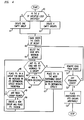
- Figure 1 shows an illustrative testing process for a sequential logic circuit which has been advantageously re-designed for increased testability with use of an illustrative embodiment of the method of the present invention.
- Figure 2A shows an example circuit to which the method of the present invention may be advantageously applied.
- Figure 2B shows the example circuit of Figure 2A after it has been advantageously re-designed for testability with use of an illustrative embodiment of the method of the present invention.
- Figure 3 shows an example circuit in which state probabilities may be estimated in accordance with an illustrative embodiment of the method of the present invention.
- Figure 4 shows a flow chart of an illustrative partitioning procedure in accordance with one illustrative embodiment of the present invention.
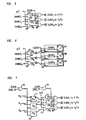
- Figure 5 shows a first illustrative implementation of an approach to clock gating in accordance with an illustrative embodiment of the present invention.
- Figure 6 shows a second illustrative implementation of an approach to clock gating in accordance with an illustrative embodiment of the present invention.
- Figure 7 shows a third illustrative implementation of an approach to clock gating in accordance with an illustrative embodiment of the present invention.
- Figure 1 shows an illustrative testing process for a sequential logic circuit which has been advantageously re-designed for increased testability with use of an illustrative embodiment of the method of the present invention.
- test generator 11 generates input stimuli and a corresponding expected output response based on a circuit description of the sequential circuit to be tested.
- the circuit design has been advantageously modified in accordance with an illustrative embodiment of the method of the present invention, as shown, for example, in Figure 4, below.
- Test generator 11 may, for example, comprise a general purpose computer system and software executing thereon.
- Each fabricated instance of circuit 12 comprises a plurality of interconnected circuit elements (e.g., gates 13 and flip-flops 18), one or more primary inputs 14 and one or more primary outputs 15.
- ATE Automatic Test Equipment
- a typical ATE system comprises hardware components (in addition to the controlling computer) which are adapted to apply stimuli to a fabricated instance of a circuit, measure the responses from the fabricated instance of the circuit, and compare the measured response to a predetermined expected response.
- the fabricated instance of the circuit to be tested is usually "plugged into” the ATE system by means of a standardized interface.
- the original design of circuit 12 has been modified so as to add circuit elements 17, three "test control inputs," and the interconnections associated therewith.
- the "CLOCK" primary input had been directly connected to the clock inputs of flip-flops 18.
- the two flip-flops (18) may be made independently controllable when the circuit is placed in a special "test mode" with use of the added N/ T ⁇ (i.e., normal mode/not test mode) primary input.
- the input stimuli generated by test generator 11 places the circuit in the test mode, and then operates the "enable” primary inputs so as to advantageously allow for independent clocking of the flip-flops as determined by the test generation process.
- flip-flops are driven by some (combinational) logic whose inputs consist of primary inputs and/or outputs of other flip-flops.
- the values of all of the flip-flops in the circuit define what is referred to as the "state" of the circuit.
- some states are more difficult to reach than others. (That is, some combinations of flip-flop values may be difficult to achieve.
- there may be unreachable states also referred to as "illegal" states.
- Hard-to-reach-states and illegal states collectively will be referred to herein as hard states. Specifically, hard states are caused by the need to drive correlated values into flip-flops which are controlled by a common clock.
- any fault whose detection requires the circuit to enter a hard state is necessarily difficult to detect -- that is, it is difficult to generate a test for such a fault. If the hard state is, in fact, illegal, then the fault is undetectable (i.e., it is impossible to generate a test for the fault).
- the detrimental correlation between flip-flops which results in difficult-to-detect faults is advantageously cancelled by transforming the common clocking into independent clocking during testing.
- detrimental relations among flip-flops are identified by finding hard states which are needed for the detection of faults.
- hard states are identified by analyzing each pair of flip-flops which are controlled by the same clock, and estimating the probability of obtaining each of the four possible combination of logic values (00, 01, 10, and 11) by a procedure described in detail below. (Such a probability of two or more lines of a circuit having a given set of values is known as a "joint line probability.") States whose probability measure is below a preselected threshold value are advantageously characterized as hard states.
- a state defined by a combination of two flip-flop values actually represents a group of 2 n-2 possible circuit states with similar properties (i.e., all states having the particular two values on the given two flip-flops in combination with one of the possible sets of values on the other n-2 flip-flops).
- the word "state” will be used herein to denote such a group of states.
- a partitioning procedure uses this information to assign flip-flops into different groups, so that the total detrimental effect of any common clocking is advantageously minimized.
- this illustrative embodiment advantageously identifies hard and needed states caused by sequentially reconvergent fanout (some hard and needed states may also be caused by loops -- in alternative embodiments of the present invention these states may also be advantageously identified).
- the correlation measure is based on the joint line probabilities for pairs of flip-flop outputs.
- computing joint line probabilities precisely is computationally complex, the following approximate method is advantageously used.
- f be a boolean function. Suppose that a random value is independently assigned to each variable x upon which f depends. Let p x be the probability that x is assigned a logic 1. There is a particular probability that f will evaluate to a logic 1 for such a randomly chosen valuation of the variables.
- the probability of f can be computed in one pass over the BDD using the following relations:
- 0,
- p x
- this computation may be advantageously performed when f is the logic driving one of the flip-flops in the circuit.
- the line probabilities of the primary inputs and of the flip-flop outputs are supplied as inputs. It may be assumed that the primary input probabilities are given (e.g., without additional information, the primary input probabilities may be assumed to be independent and uniform -- thus, p x may be assigned a value of .5 when x is a primary input), and the flip-flop output probabilities may be advantageously estimated using conventional techniques such as that presented in J. Monteiro, S. Devadas, and B. Lin, "A Methodology for Efficient Estimation of Switching Activity in Sequential Logic Circuits," Proc.
- the first of the above probabilities i.e., 0
- the precise value for the probability of each of the latter three combinations is actually 1/3.
- BDDs cannot be built for some of the flip-flops in a given circuit -- in such a case a flip-flop probability of 0.5 may be arbitrarily assumed, although this assumption may result in not identifying some of the hard states.
- flip-flop probabilities may be computed by conventional simulation techniques using random input vectors. That is, a large number of randomly chosen input vectors are applied to the circuit, and for each flip-flop, the frequency with which the flip-flop obtains each of the two logic values is determined.
- Such simulation techniques are familiar to those of ordinary skill in the art.
- the probability P S of state S may then be used as a measure of the difficulty of reaching state S .
- S is said be hard (i.e ., difficult-to-reach) if P S is below a preselected threshold value, such as, for example, 0.1.
- N S denote the number of faults that require S for their detection. If N s > 0, then S is a hard and needed state.
- FIG. 4 shows an illustrative partitioning procedure in accordance with one embodiment of the present invention.
- This partitioning procedure can operate in either of two modes.
- the first mode it attempts to create as many groups with independent clocks as are needed to reduce DE F to 0. Therefore, the number of groups, K, is bounded only by the number of flip-flops in the circuit.
- the user-specified K could be provided (or determined) a priori, and the first mode could be avoided altogether.
- the circuit may be advantageously modeled by a graph where each vertex (i.e ., node) represents one flip-flop in the circuit.
- An edge (A,B) exists between two flip-flops A and B, if and only if DE AB > 0, i.e., the combination of flip-flops A and B contributes to the hard and needed states.
- a weight of DE AB is assigned to each edge. Initially each group is empty. At the completion of the procedure, however, each flip-flop in the circuit is assigned to a group.
- the illustrative procedure of Figure 4 processes each of the edges of the graph in decreasing weight order as follows. For each unassigned flip-flop of the edge being processed, the procedure places the flip-flop in its "most favorable" group (if it has not already been assigned). A group G is said to be most favorable to flip-flop A, if placing A in G introduces a minimal increase in DE G as compared to placing A in other groups. In the first of the aforementioned modes, where the user has not specified a maximum number of groups, no increase is acceptable (i.e ., the "minimal" increase must equal 0), since, in this mode, the goal is to reduce DE F to zero -- if no such group is found, a new group is created and the flip-flop is placed therein.
- decision 40 initially determines which of the two aforementioned modes is being used. If the procedure is operating in the mode in which the user has not specified a maximum number of groups, step 41 creates one initial group. Otherwise, step 42 creates the user-specified number of groups, K. Then in step 43 the edges of the graph are rank ordered by their weights, and the first iteration of the primary execution loop begins.
- step 44 The edge with the maximum weight is selected in step 44, and that edge is checked to identify a flip-flop i of that edge, which flip-flop has not yet been assigned to a group (decision 45). Assuming such a flip-flop is identified, the processing continues differently based on the mode in which the process is operating (decision 46). If the number of groups was not user-specified, step 48 places flip-flop i in a group, G , for which no increase in the group's detrimental effect value, DE G , results therefrom, if any such group can be found. If there is no such group (decision 49), a new group is created for flip-flop i in step 50.
- step 47 places flip-flop i in the "most favorable" group -- i.e., the group for which a minimum increase in its detrimental effect value, DE G , results from adding flip-flop i thereto.
- step 51 After flip-flop i has been assigned to a group, flow returns to decision 45 to continue processing for any other unassigned flip-flop of the given edge, if any. If all (i.e., both) of the flip-flops of that edge have been assigned, the edge is removed from the graph in step 51, and decision 52 determines if there are more edges to process. If so, control returns to the beginning of the primary loop (i.e., step 44). If not, step 53 places any remaining (i.e., unassigned) flip-flops into arbitrary groups.
- the flip-flops of a given circuit are partitioned into several groups, such that each group may be advantageously controlled by an independent clock during testing.
- this may be achieved by gating the original clock signal based on a first illustrative implementation as shown in Figure 5.
- signal N/ T ⁇ is set to a logic 0 value, thereby enabling the independent operation of each clock signal, CLOCK i , based on its corresponding enabling signal, ENABLE i .
- this DFT technique advantageously does not introduce any delay penalty.
- this implementation may, in some cases, lead to clock skew problems, since the original clock distribution is modified by the addition of gates 57, 58 and 59, and the fanout therefrom.
- FIG. 6 shows a second illustrative implementation in accordance with an illustrative embodiment of the present invention, which implementation overcomes the potential clock skewing problem by distributing the enabling signals rather than the gated clocks, and by placing clock gating AND gates 64, 65 and 66 adjacent to the controlled flip-flops. That is, in this case, enabling gates 61, 62 and 63 provide the fanout to each corresponding group of flip-flops. Therefore, the routing of the original CLOCK signal need not be changed, and the potential clock skew problem may thereby be advantageously avoided. Note that in a standard-cell ASIC (Application Specific Integrated Circuit) circuit implementation, it may be advantageous to provide the clock control gate as part of the flip-flop cell itself.
- ASIC Application Specific Integrated Circuit
- Figure 7 shows a third illustrative implementation of an approach to clock gating in accordance with an illustrative embodiment of the present invention, which implementation advantageously overcomes this problem by introducing K additional flip-flops (flip-flops 71, 72 and 73 in the figure) in which the enabling values may be temporarily stored.
- signal N/ T ⁇ is held at a logic 1 value
- signal LOAD_EV load enabling value
- CLOCK i CLOCK
- the enabling values may be advantageously loaded by setting signal LOAD_EV to a logic 1, which also ensures that the CLOCK i signals are inactive for all the flip-flops in the original circuit, by disabling AND gates 78, 79 and 80 (due to AND gate 74). Therefore, the state of the circuit does not change during the loading process.
- the test generator can advantageously generate sequences assuming that each clock has an individual enabling primary input. Then, after the test sequences have been generated, one additional vector is inserted therein to load the appropriate set of enabling values whenever the set of active clocks changes.
- the approaches of the illustrative implementations shown in Figures 6 and 7 may be advantageously combined to both reduce additional pin requirements and to avoid clock skew problems.
- the cost (i.e., in additional components and pins) of applying this illustrative third implementation and avoiding clock skew is 2 primary inputs, K enable flip-flops, K OR gates, and N+ 2 AND gates.
- edges in the graph which represent pairs of flip-flops, may easily be replaced by generalized n-tuples of flip-flops. Otherwise the procedure operates in essentially the same manner as described above and shown in Figure 4.
- the method of the present invention may be advantageously combined with other DFT methods.
- clock partitioning alone may be inadequate if used on a circuit that is not initializable.
- Such conventional DFT methods include, for example, partial or full scan, the use of partial reset, and the use of partial observation techniques, each of which is familiar to those of ordinary skill in the art.
- partial reset a subset of the flip-flops receive an additional primary input which is used as a direct set or reset signal.
- partial observation a subset of flip-flops are typically XOR'd together and connected to one additional output.
- partial reset and partial observation flip-flops may be based on any of a number of conventional methods, such as, for example, those presented in P. Parikh and M. Abramovici, "On Combining DFT Techniques", Proc. Int'l. Test Conf., pp. 423-429, 1995. Note also that when partial observation is used, the flip-flops can be observed either at the D-input or at the Q-output.
- the techniques of the present invention are advantageously combined with certain other DFT techniques as follows: first, partial reset techniques are applied to the original circuit; second, partial observation techniques are applied to the circuit resultant therefrom; and third, the illustrative method described above in accordance with the present invention is applied to the circuit which results from the application of both the partial reset and the partial observation techniques.
- each set of flip-flops sharing a common clock line may, for example, be individually partitioned according to the principles and methods described above.
Landscapes
- Engineering & Computer Science (AREA)
- General Engineering & Computer Science (AREA)
- Physics & Mathematics (AREA)
- General Physics & Mathematics (AREA)
- Tests Of Electronic Circuits (AREA)
- Test And Diagnosis Of Digital Computers (AREA)
- Design And Manufacture Of Integrated Circuits (AREA)
Applications Claiming Priority (2)
| Application Number | Priority Date | Filing Date | Title |
|---|---|---|---|
| US637026 | 1996-04-24 | ||
| US08/637,026 US5625630A (en) | 1996-04-24 | 1996-04-24 | Increasing testability by clock transformation |
Publications (1)
| Publication Number | Publication Date |
|---|---|
| EP0803814A1 true EP0803814A1 (de) | 1997-10-29 |
Family
ID=24554239
Family Applications (1)
| Application Number | Title | Priority Date | Filing Date |
|---|---|---|---|
| EP97302563A Withdrawn EP0803814A1 (de) | 1996-04-24 | 1997-04-15 | Verbesserte Prüfbarkeit durch Takt-Transformation |
Country Status (4)
| Country | Link |
|---|---|
| US (1) | US5625630A (de) |
| EP (1) | EP0803814A1 (de) |
| JP (1) | JPH1049567A (de) |
| CA (1) | CA2197815A1 (de) |
Families Citing this family (27)
| Publication number | Priority date | Publication date | Assignee | Title |
|---|---|---|---|---|
| US5748646A (en) * | 1996-02-02 | 1998-05-05 | Matsushita Electric Industrial Co., Ltd. | Design-for-testability method for path delay faults and test pattern generation method for path delay faults |
| US5875196A (en) * | 1997-01-03 | 1999-02-23 | Nec Usa, Inc. | Deriving signal constraints to accelerate sequential test generation |
| FR2773652B1 (fr) * | 1998-01-14 | 2002-10-11 | Sgs Thomson Microelectronics | Circuit de generation d'un signal d'activation commande |
| US6823486B2 (en) | 2000-06-05 | 2004-11-23 | Fujitsu Limited | Automatic test pattern generation for functional register transfer level circuits using assignment decision diagrams |
| US7073143B1 (en) * | 2000-11-06 | 2006-07-04 | Cadence Design Systems, Inc. | Solving constraint satisfiability problem for circuit designs |
| US6728917B2 (en) | 2001-02-09 | 2004-04-27 | Agere Systems Inc. | Sequential test pattern generation using combinational techniques |
| US7017096B2 (en) * | 2002-03-26 | 2006-03-21 | Agere Systems Inc. | Sequential test pattern generation using clock-control design for testability structures |
| US7127695B2 (en) * | 2002-07-18 | 2006-10-24 | Incentia Design Systems Corp. | Timing based scan chain implementation in an IC design |
| US7124342B2 (en) * | 2004-05-21 | 2006-10-17 | Syntest Technologies, Inc. | Smart capture for ATPG (automatic test pattern generation) and fault simulation of scan-based integrated circuits |
| JP4562136B2 (ja) * | 2003-11-19 | 2010-10-13 | 財団法人北九州産業学術推進機構 | グラフ幅削減装置及びグラフ幅削減方法、並びに論理回路合成装置及び論理回路合成方法 |
| US7231615B2 (en) * | 2003-12-08 | 2007-06-12 | Cadence Design Systems, Inc. | Methods and apparatus for transforming sequential logic designs into equivalent combinational logic |
| JP4752029B2 (ja) * | 2005-03-30 | 2011-08-17 | 国立大学法人九州工業大学 | 半導体論理回路装置のテスト方法及びテストプログラム |
| WO2007013306A1 (ja) * | 2005-07-26 | 2007-02-01 | Kyushu Institute Of Technology | 半導体論理回路装置のテストベクトル生成方法及びテストベクトル生成プログラム |
| WO2013100783A1 (en) | 2011-12-29 | 2013-07-04 | Intel Corporation | Method and system for control signalling in a data path module |
| US10331583B2 (en) | 2013-09-26 | 2019-06-25 | Intel Corporation | Executing distributed memory operations using processing elements connected by distributed channels |
| KR20170025447A (ko) * | 2015-08-28 | 2017-03-08 | 삼성전자주식회사 | 클락 파워를 줄일 수 있는 집적 회로를 설계하는 방법 |
| US11086816B2 (en) | 2017-09-28 | 2021-08-10 | Intel Corporation | Processors, methods, and systems for debugging a configurable spatial accelerator |
| US10502782B2 (en) | 2017-11-10 | 2019-12-10 | International Business Machines Corporation | Synthesis for random testability using unreachable states in integrated circuits |
| US11307873B2 (en) | 2018-04-03 | 2022-04-19 | Intel Corporation | Apparatus, methods, and systems for unstructured data flow in a configurable spatial accelerator with predicate propagation and merging |
| US10891240B2 (en) | 2018-06-30 | 2021-01-12 | Intel Corporation | Apparatus, methods, and systems for low latency communication in a configurable spatial accelerator |
| US11200186B2 (en) | 2018-06-30 | 2021-12-14 | Intel Corporation | Apparatuses, methods, and systems for operations in a configurable spatial accelerator |
| US10853073B2 (en) | 2018-06-30 | 2020-12-01 | Intel Corporation | Apparatuses, methods, and systems for conditional operations in a configurable spatial accelerator |
| US10817291B2 (en) | 2019-03-30 | 2020-10-27 | Intel Corporation | Apparatuses, methods, and systems for swizzle operations in a configurable spatial accelerator |
| US10915471B2 (en) | 2019-03-30 | 2021-02-09 | Intel Corporation | Apparatuses, methods, and systems for memory interface circuit allocation in a configurable spatial accelerator |
| US11037050B2 (en) | 2019-06-29 | 2021-06-15 | Intel Corporation | Apparatuses, methods, and systems for memory interface circuit arbitration in a configurable spatial accelerator |
| US12086080B2 (en) | 2020-09-26 | 2024-09-10 | Intel Corporation | Apparatuses, methods, and systems for a configurable accelerator having dataflow execution circuits |
| US12340155B2 (en) * | 2022-04-29 | 2025-06-24 | Synopsys, Inc. | Detecting instability in combinational loops in electronic circuit designs |
Family Cites Families (3)
| Publication number | Priority date | Publication date | Assignee | Title |
|---|---|---|---|---|
| JPH03201035A (ja) * | 1989-10-24 | 1991-09-02 | Matsushita Electric Ind Co Ltd | 検査系列生成方法 |
| US5450415A (en) * | 1992-11-25 | 1995-09-12 | Matsushita Electric Industrial Co., Ltd. | Boundary scan cell circuit and boundary scan test circuit |
| US5513123A (en) * | 1994-06-30 | 1996-04-30 | Nec Usa, Inc. | Non-scan design-for-testability of RT-level data paths |
-
1996
- 1996-04-24 US US08/637,026 patent/US5625630A/en not_active Expired - Lifetime
-
1997
- 1997-02-18 CA CA002197815A patent/CA2197815A1/en not_active Abandoned
- 1997-04-14 JP JP9095433A patent/JPH1049567A/ja active Pending
- 1997-04-15 EP EP97302563A patent/EP0803814A1/de not_active Withdrawn
Non-Patent Citations (6)
| Title |
|---|
| ABRAMOVICI M ET AL: "THE BEST FLIP-FLOPS TO SCAN", PROCEEDINGS OF THE INTERNATIONAL TEST CONFERENCE, NASHVILLE, OCT. 28 - 30, 1991, 1 January 1991 (1991-01-01), INSTITUTE OF ELECTRICAL AND ELECTRONICS ENGINEERS, pages 166 - 173, XP000272247 * |
| AGRAWAL V.D., SETH S.C., DEOGUN J.S.: "Design for testability and test generation with two clocks.", 4TH CSI/IEEE INTERNATIONAL SYMPOSIUM ON VLSI DESIGN, 4 January 1994 (1994-01-04) - 8 January 1994 (1994-01-08), NEW DELHI, INDIA, pages 112 - 117, XP002035831 * |
| EINSPAHR K.L., SETH S.C., AGRAWAL V.D.: "Improving circuit testability by clock control", 6TH GREAT LAKES SYMPOSIUM ON VLSI, 22 March 1996 (1996-03-22) - 23 March 1996 (1996-03-23), AMES, IA, USA, pages 288 - 293, XP002035829 * |
| LONG D.E.,IYER M.A., ABRAMOVICI M.: "Identifying sequentially untestable faults using illegal states", 13TH VLSI TEST SYMPOSIUM, 30 April 1995 (1995-04-30) - 3 May 1995 (1995-05-03), PRINCETON,NJ,USA, pages 4 - 11, XP002035830 * |
| RAJAN K.B., LONG D.E., ABRAMOVICI M.: "Increasing testability by clock transformation (Getting Rid of Those Darn States)", 14TH IEEE VLSI TEST SYMPOSIUM, 28 April 1996 (1996-04-28) - 1 May 1996 (1996-05-01), PRINCETON, NJ, USA, pages 224 - 230, XP002035832 * |
| WEN-CHANG FANG ET AL: "CLOCK GROUPING: A LOW COST DFT METHODOLOGY FOR DELAY TESTING", PROCEEDINGS OF THE DESIGN AUTOMATION CONFERENCE, SAN DIEGO, JUNE 6 - 10, 1994, no. CONF. 31, 6 June 1994 (1994-06-06), INSTITUTE OF ELECTRICAL AND ELECTRONICS ENGINEERS, pages 94 - 99, XP000488987 * |
Also Published As
| Publication number | Publication date |
|---|---|
| US5625630A (en) | 1997-04-29 |
| CA2197815A1 (en) | 1997-10-25 |
| JPH1049567A (ja) | 1998-02-20 |
Similar Documents
| Publication | Publication Date | Title |
|---|---|---|
| US5625630A (en) | Increasing testability by clock transformation | |
| Edirisooriya et al. | Diagnosis of scan path failures | |
| Agrawal et al. | Combinational ATPG theorems for identifying untestable faults in sequential circuits | |
| US5043986A (en) | Method and integrated circuit adapted for partial scan testability | |
| US5748497A (en) | System and method for improving fault coverage of an electric circuit | |
| US5132974A (en) | Method and apparatus for designing integrated circuits for testability | |
| US7644333B2 (en) | Restartable logic BIST controller | |
| US5448576A (en) | Boundary scan architecture extension | |
| Ghosh et al. | Design for hierarchical testability of RTL circuits obtained by behavioral synthesis | |
| US5257268A (en) | Cost-function directed search method for generating tests for sequential logic circuits | |
| JPH04278475A (ja) | 先読みパターン発生及びシミュレーションの方法及びシステム | |
| Wen et al. | A highly-guided X-filling method for effective low-capture-power scan test generation | |
| US5640402A (en) | Fast flush load of LSSD SRL chains | |
| JP2002286810A (ja) | スキャン方式3重み加重ランダムス・ビルトイン・セルフテストのテストセット生成方法、スキャン方式ビルトイン・セルフテスト回路 | |
| Lin et al. | Pseudofunctional testing | |
| US5566187A (en) | Method for identifying untestable faults in logic circuits | |
| JP4024707B2 (ja) | クロック制御式テスト容易化デザイン構成を用いたシーケンシャルテストパターン生成 | |
| EP1327890B1 (de) | Optimierungsverfahren einer Vielzahl von Tests für digitale integrierte Schaltungen | |
| US6334200B1 (en) | Testable integrated circuit, integrated circuit design-for-testability method, and computer-readable medium storing a program for implementing the design-for-testability method | |
| Chen et al. | Overall consideration of scan design and test generation | |
| US5691990A (en) | Hybrid partial scan method | |
| Pomeranz et al. | Application of homing sequences to synchronous sequential circuit testing | |
| US6728917B2 (en) | Sequential test pattern generation using combinational techniques | |
| US6920597B2 (en) | Uniform testing of tristate nets in logic BIST | |
| EP0342787A2 (de) | Suchverfahren zur Prüfvektorerzeugung für sequentielle Logikschaltungen |
Legal Events
| Date | Code | Title | Description |
|---|---|---|---|
| PUAI | Public reference made under article 153(3) epc to a published international application that has entered the european phase |
Free format text: ORIGINAL CODE: 0009012 |
|
| AK | Designated contracting states |
Kind code of ref document: A1 Designated state(s): DE FR GB IT |
|
| 17P | Request for examination filed |
Effective date: 19980416 |
|
| STAA | Information on the status of an ep patent application or granted ep patent |
Free format text: STATUS: THE APPLICATION HAS BEEN WITHDRAWN |
|
| 18W | Application withdrawn |
Withdrawal date: 19990203 |