EP0802619B1 - Vorrichtung mit gestapelten Thyristoren und Freilaufdioden - Google Patents
Vorrichtung mit gestapelten Thyristoren und Freilaufdioden Download PDFInfo
- Publication number
- EP0802619B1 EP0802619B1 EP97400840A EP97400840A EP0802619B1 EP 0802619 B1 EP0802619 B1 EP 0802619B1 EP 97400840 A EP97400840 A EP 97400840A EP 97400840 A EP97400840 A EP 97400840A EP 0802619 B1 EP0802619 B1 EP 0802619B1
- Authority
- EP
- European Patent Office
- Prior art keywords
- thyristor
- anode
- cathode
- drl
- cooling device
- Prior art date
- Legal status (The legal status is an assumption and is not a legal conclusion. Google has not performed a legal analysis and makes no representation as to the accuracy of the status listed.)
- Expired - Lifetime
Links
- 238000001816 cooling Methods 0.000 claims description 104
- 239000004065 semiconductor Substances 0.000 claims description 26
- 230000004224 protection Effects 0.000 claims description 13
- 239000003990 capacitor Substances 0.000 claims description 5
- 239000004020 conductor Substances 0.000 claims 11
- 230000008520 organization Effects 0.000 claims 2
- 238000010586 diagram Methods 0.000 description 6
- 230000008901 benefit Effects 0.000 description 4
- 230000009850 completed effect Effects 0.000 description 2
- 230000002441 reversible effect Effects 0.000 description 2
- 230000004087 circulation Effects 0.000 description 1
- 239000002131 composite material Substances 0.000 description 1
- 239000012212 insulator Substances 0.000 description 1
- 239000007788 liquid Substances 0.000 description 1
- 238000004519 manufacturing process Methods 0.000 description 1
- 230000004048 modification Effects 0.000 description 1
- 238000012986 modification Methods 0.000 description 1
- 230000000717 retained effect Effects 0.000 description 1
Images


Classifications
-
- H—ELECTRICITY
- H02—GENERATION; CONVERSION OR DISTRIBUTION OF ELECTRIC POWER
- H02M—APPARATUS FOR CONVERSION BETWEEN AC AND AC, BETWEEN AC AND DC, OR BETWEEN DC AND DC, AND FOR USE WITH MAINS OR SIMILAR POWER SUPPLY SYSTEMS; CONVERSION OF DC OR AC INPUT POWER INTO SURGE OUTPUT POWER; CONTROL OR REGULATION THEREOF
- H02M7/00—Conversion of AC power input into DC power output; Conversion of DC power input into AC power output
- H02M7/42—Conversion of DC power input into AC power output without possibility of reversal
- H02M7/44—Conversion of DC power input into AC power output without possibility of reversal by static converters
- H02M7/48—Conversion of DC power input into AC power output without possibility of reversal by static converters using discharge tubes with control electrode or semiconductor devices with control electrode
- H02M7/505—Conversion of DC power input into AC power output without possibility of reversal by static converters using discharge tubes with control electrode or semiconductor devices with control electrode using devices of a thyratron or thyristor type requiring extinguishing means
- H02M7/515—Conversion of DC power input into AC power output without possibility of reversal by static converters using discharge tubes with control electrode or semiconductor devices with control electrode using devices of a thyratron or thyristor type requiring extinguishing means using semiconductor devices only
- H02M7/519—Conversion of DC power input into AC power output without possibility of reversal by static converters using discharge tubes with control electrode or semiconductor devices with control electrode using devices of a thyratron or thyristor type requiring extinguishing means using semiconductor devices only in a push-pull configuration
-
- H—ELECTRICITY
- H02—GENERATION; CONVERSION OR DISTRIBUTION OF ELECTRIC POWER
- H02M—APPARATUS FOR CONVERSION BETWEEN AC AND AC, BETWEEN AC AND DC, OR BETWEEN DC AND DC, AND FOR USE WITH MAINS OR SIMILAR POWER SUPPLY SYSTEMS; CONVERSION OF DC OR AC INPUT POWER INTO SURGE OUTPUT POWER; CONTROL OR REGULATION THEREOF
- H02M7/00—Conversion of AC power input into DC power output; Conversion of DC power input into AC power output
- H02M7/003—Constructional details, e.g. physical layout, assembly, wiring or busbar connections
Definitions
- the present invention relates to semiconductor devices of power as well as their devices electrical interface, in general, and door, more particularly on a stacked device thyristors and freewheeling diodes.
- the semiconductor elements of power one can quote the thyristors, the diodes and freewheeling diodes.
- These power semiconductor elements are cooled by means of cooling devices dissipating heat by circulation of a liquid cooling.
- Each of the power semiconductor elements are sandwiched between two holding elements, one or both of the holding elements holding can be a cooling device.
- the holding means ensures electrical continuity between two semiconductor elements power or between a semiconductor element of power and a protection circuit.
- Power semiconductor element assemblies and holding elements may be different due to that they derive from the retained electrical diagram.
- An object of the invention is therefore a device for stack of thyristors and freewheeling diodes, allowing a single wiring whatever the function power of the power semiconductor device.
- Another object of the invention is a device for stack of thyristors and freewheeling diodes, requiring a minimum of cooling devices.
- the stacking device GTO thyristors and DRL freewheeling diodes for semiconductor device said stacking device having electrical supply connection terminals + HT, -HT and PM output of said stacking device, said stacking device, is characterized in that the geometrical arrangement of the wiring of said terminals of electrical connection + HT, PM and -HT is predetermined from way to allow to modify the arrangement of said GTO thyristors and said DRL freewheeling diodes in said stack in order to obtain different functions of the semiconductor device.
- An advantage of the stacking device of the invention is the use of electrical connection means standard, for example a bus bar, to connect electrically the stacking device and the circuit protection of this device.
- Another advantage of the stacking device the invention is the possibility of optimizing the number of cooling devices while maintaining a single connection for several applications of the device semiconductor.
- Another advantage of the stacking device the invention is the realization of a line of products standards of the mixed bridge type with forced switching or of the type inverter.
- Another advantage of the stacking device the invention is the production of standard products with high thermal power or less thermal power always keeping a unique connection.
- the GTO thyristor stacking device, DRL freewheel diodes and D diodes of the invention is for semiconductor devices of the type converter.
- the stacking device has terminals for electrical connection of power + HT, -HT and output PM.
- the stacking device is completed by electrical connection terminals Cs, Cc between diodes Ds, Dc and a protection circuit P.
- the stacking device is such that the geometrical arrangement of the wiring of the connection terminals electric + HT, PM and -HT is predetermined.
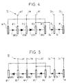
- the device to stack 1A for mixed bridge with forced switching includes successively a first cooling device R1, a first thyristor GTOs, a second device for R2 cooling, a first free-wheeling diode DRLs, a third cooling device R3, a second DRLi freewheeling diode, a fourth cooling R4, a second thyristor GTOi and a fifth cooling device R5.
- the cathode of the first GTOs thyristor is connected to the PM terminal.
- the cathode of the second thyristor GTOi is connected to the potential -HT.
- the anode of the first free-wheeling diode DRLs is connected to the PM terminal.
- the anode of the first GTOs thyristor is connected to the potential + HT.
- the anode of the second thyristor GTOi is connected to the terminal PM.
- the + HV connection terminal is connected to the cathode of the first free-wheeling diode DRLs and at the anode of the first thyristor GTOs.
- the anode of the second thyristor GTO'i is connected to the PM terminal.
- the anode of the second free-wheeling diode DRL'i is connected to the potential -HT.
- connection terminal -HT is connected to the cathode of the second thyristor GTO'i and at the anode of the second diode of DRL'i freewheel.
- the device to 1D stack for inverter successively has a first cooling device R'1, a first thyristor GTO's, a second cooling device R'2, a first free-wheeling diode DRL's, a first conductive element M'1, a second freewheeling diode DRL'i, a third cooling device R'3, a second thyristor GTO'i and a third device for cooling R'5.
- the anode of the first GTO's thyristor is connected to the potential + HT.
- the anode of the first free-wheeling diode DRL's is connected to the PM terminal.
- the cathode of the second free-wheeling diode DRL'i is connected to the PM terminal.
- GTO s thyristor cathode is connected to terminal PM.
- the cathode of the second freewheeling diode DRL "i is connected to the PM terminal.
- the device to 1F stack for chopper successively has a first conductive element M "1, a first wheel diode free DRL “s, a first cooling device R” 1, a GTO “s thyristor, a second cooling R “2, an insulating element I", a third cooling device R “3, a second wheel diode free DRL “i and a fourth cooling device R "4.
- the + HV connection terminal is connected to the cathode of the first free-wheeling diode DRL “s and at the anode of thyristor GTO "s.
- connection terminal -HT is connected to the anode of the second freewheeling diode DRL "i.
- the cathode of the first diode Ds is connected to the potential -HT.
- the anode of the first diode Ds and the cathode of the second diode Dc are connected to the terminal Cs.
- the anode of the second diode Dc is connected to the terminal CC.
- a capacitance Cs of the protection circuit P is disposed between the PM output electrical connection terminal and the common terminal Cs of the first Ds and second diode Dc.
- the third cooling devices R “3 (figure 7) and the third R “3 or fourth R” 4 devices cooling (figure 8) can be replaced by conductive elements in the case of a thermal power at transmit less.
Landscapes
- Engineering & Computer Science (AREA)
- Power Engineering (AREA)
- Inverter Devices (AREA)
- Rectifiers (AREA)
- Power Conversion In General (AREA)
Claims (12)
- Vorrichtung mit gestapelten Thyristoren (GTO) und Freilaufdioden (DRL) für Halbleitervorrichtungen, wobei die genannte Stapelvorrichtung Stromversorgungsanschlüsse +HT, -HT und einen Ausgangsanschluss PM der genannten Stapelvorrichtung aufweist, sowie Kühlvorrichtungen, wobei die Dioden (DRL) und die Thyristoren (GTO) jeweils im Stapel zwischen den Kühlvorrichtungen eingefügt sind, dadurch gekennzeichnet, dass die geometrische Anordnung der Kühlvorrichtungen im Stapel und der Verkabelung der Anschlussklemmen unverändert ist und die Anordnung der Freilaufdioden und der Thyristoren zwischen den Kühlvorrichtungen im Stapel in Abhängigkeit vom Typ der Halbleitervorrichtung veränderlich ist.
- Vorrichtung (1A) nach Patentanspruch 1 für Wandler, nacheinander eine erste Kühlvorrichtung (R1) aufweisend, einen ersten Thyristor (GTOs), eine zweite Kühlvorrichtung (R2), eine erste Freilaufdiode (DRLs), eine dritte Kühlvorrichtung (R3), eine zweite Freilaufdiode (DRLi), eine vierte Kühlvorrichtung (R4), einen zweiten Thyristor (GTOi) und eine fünfte Kühlvorrichtung (R5), wobei die genannte Anschlussklemme (+HT) mit der Anode des ersten Thyristors (GTOs) und der Kathode der ersten Freilaufdiode (DRLs) verbunden ist, die genannte Anschlussklemme (PM) mit der Anode der genannten ersten Freilaufdiode (DRLs) verbunden ist und mit der Kathode der zweiten Freilaufdiode (DRLi), sowie mit der Kathode des genannten ersten Thyristors (GTOs) und der Anode des zweiten Thyristors (GTOi), wobei die genannte Anschlussklemme (-HT) mit der Anode der genannten zweiten Freilaufdiode (DRLi) und der Kathode des genannten zweiten Thyristors (GTOi) verbunden ist.
- Vorrichtung (1A) nach Patentanspruch 2, in der die dritte Kühlvorrichtung R3 durch ein Leiterelement M ersetzt ist.
- Vorrichtung (1B) nach Patentanspruch 1 für Wandler, nacheinander eine erste Kühlvorrichtung R1 aufweisend, eine erste Freilaufdiode DRLs, eine zweite Kühlvorrichtung R2, einen ersten Thyristor GTOs, eine dritte Kühlvorrichtung R3, einen zweiten Thyristor GTOi, eine vierte Kühlvorrichtung R4, eine zweite Freilaufdiode DRLi und eine fünfte Kühlvorrichtung R5, wobei die genannte Anschlussklemme +HT mit der Kathode der ersten Freilaufdiode DRLs und der Anode des ersten Thyristors GTOs verbunden ist, die genannte Anschlussklemme PM mit der Kathode des genannten ersten Thyristors GTOs verbunden ist und mit der Anode des zweiten Thyristors GTOi, sowie mit der Anode der genannten ersten Freilaufdiode DRLs und der Kathode der zweiten Freilaufdiode DRLi, während die genannte Anschlussklemme -HT mit der Kathode des genannten zweiten Thyristors GTOi und der Anode der genannten zweiten Freilaufdiode DRLi verbunden ist.
- Vorrichtung (1B) nach Patentanspruch 4, in der die erste Kühlvorrichtung R1 und die fünfte R5 durch Leiterelemente M ersetzt sind.
- Vorrichtung (1C) nach Patentanspruch 1 für Wandler, nacheinander ein erstes Leiterelement M'1 aufweisend, eine erste Freilaufdiode DRL's, eine erste Kühlvorrichtung R'1, einen ersten Thyristor GTO's, eine zweite Kühlvorrichtung R'2, einen zweiten Thyristor GTO'i, eine dritte Kühlvorrichtung R'3, eine zweite Freilaufdiode DRL'i und ein zweites Leiterelement M'2, wobei die genannte Anschlussklemme +HT mit der Kathode der ersten Freilaufdiode DRL's und der Anode des ersten Thyristors GTO's verbunden ist, die genannte Anschlussklemme PM mit der Kathode des genannten ersten Thyristors GTO's verbunden ist und mit der Anode des zweiten Thyristors GTO'i, sowie mit der Anode der genannten ersten Freilaufdiode DRL's und der Kathode der zweiten Freilaufdiode DRL'i, während die genannte Anschlussklemme -HT mit der Kathode des genannten zweiten Thyristors GTO'i und der Anode der genannten zweiten Freilaufdiode DRL'i verbunden ist.
- Vorrichtung (1D) nach Patentanspruch 1 für Wandler, nacheinander eine erste Kühlvorrichtung R'1 aufweisend, einen ersten Thyristor GTO's, eine zweite Kühlvorrichtung R'2, eine erste Freilaufdiode DRL's, ein erstes Leiterelement M'1, eine zweite Freilaufdiode DRL'i, eine dritte Kühlvorrichtung R'3, einen zweiten Thyristor GTO'i und eine vierte Kühlvorrichtung R'4, wobei die genannte Anschlussklemme +HT mit der Anode des ersten Thyristors GTO's und der Kathode der ersten Freilaufdiode DRL's verbunden ist, die genannte Anschlussklemme PM mit der Anode der genannten ersten Freilaufdiode DRL's verbunden ist und mit der Kathode der zweiten Freilaufdiode DRL'i, sowie mit der Kathode des genannten ersten Thyristors GTO's und der Anode des zweiten Thyristors GTO'i, während die genannte Anschlussklemme -HT mit der Anode der genannten zweiten Freilaufdiode DRL'i und der Kathode des genannten zweiten Thyristors GTO'i verbunden ist.
- Vorrichtung (1E) nach Patentanspruch 1 für Wandler, nacheinander ein erstes Leiterelement M''1 aufweisend, eine erste Freilaufdiode DRL''s, eine erste Kühlvorrichtung R''1, einen Thyristor GTO''s, eine zweite Kühlvorrichtung R''2, eine zweite Freilaufdiode DRL''i, eine dritte Kühlvorrichtung R''3, ein Isolationselement I'' und ein zweites Leiterelement M''2, wobei die genannte Anschlussklemme +HT mit der Kathode der ersten Freilaufdiode DRL''s und der Anode des Thyristors GTO"s verbunden ist, die genannte Anschlussklemme PM mit der Kathode des genannten ersten Thyristors GTO''s verbunden ist und mit der Kathode der zweiten Freilaufdiode DRL''i, sowie mit der Anode der genannten ersten Freilaufdiode DRL''s, während die genannte Anschlussklemme -HT mit der Anode der genannten zweiten Freilaufdiode DRL''i verbunden ist.
- Vorrichtung (1E) nach Patentanspruch 8, in der die dritte Kühlvorrichtung R''3 durch ein Leiterelement ersetzt ist.
- Vorrichtung (1F) nach Patentanspruch 1 für Wandler, nacheinander ein erstes Leiterelement M''1 aufweisend, eine erste Freilaufdiode DRL''s, eine erste Kühlvorrichtung R''1, einen Thyristor GTO''s, eine zweite Kühlvorrichtung R''2, ein Isolationselement I'', eine dritte Kühlvorrichtung R''3, eine zweite Freilaufdiode DRL''i und eine vierte Kühlvorrichtung R''4, wobei die genannte Anschlussklemme +HT mit der Kathode der ersten Freilaufdiode DRL"s und der Anode des Thyristors GTO''s verbunden ist, die genannte Anschlussklemme PM mit der Kathode des genannten Thyristors GTO''s verbunden ist, sowie mit der Anode der genannten ersten Freilaufdiode DRL''s und mit der Kathode der zweiten Freilaufdiode DRL''i, während die genannte Anschlussklemme -HT mit der Anode der genannten zweiten Freilaufdiode DRL''i verbunden ist.
- Vorrichtung (1F) nach Patentanspruch 10, in der die dritte Kühlvorrichtung R''3 oder die vierte Kühlvorrichtung R''4 durch ein Leiterelement ersetzt ist.
- Vorrichtung nach irgendeinem der Patentansprüche 1 bis 11, die vervollständigt wird durch nacheinander eine erste Diode Ds, eine Kühlvorrichtung R, eine zweite Diode Dc und ein Leiterelement M, wobei die genannte erste Diode Ds und die zweite Dc durch die Spannung der Potentiale -HT und +HT über einen Kondensator Cc einer Schutzschaltung P invers vorgespannt sind, wobei ein Kondensator Cs der genannten Schutzschaltung P zwischen der genannten Ausgangsklemme PM und der gemeinsamen Klemme Cs der genannten ersten Diode Ds und der zweiten Dc angeordnet ist.
Applications Claiming Priority (2)
| Application Number | Priority Date | Filing Date | Title |
|---|---|---|---|
| FR9604870 | 1996-04-18 | ||
| FR9604870A FR2747857B1 (fr) | 1996-04-18 | 1996-04-18 | Dispositif a empilement de thyristors et de diodes de roue libre |
Publications (2)
| Publication Number | Publication Date |
|---|---|
| EP0802619A1 EP0802619A1 (de) | 1997-10-22 |
| EP0802619B1 true EP0802619B1 (de) | 2001-12-05 |
Family
ID=9491341
Family Applications (1)
| Application Number | Title | Priority Date | Filing Date |
|---|---|---|---|
| EP97400840A Expired - Lifetime EP0802619B1 (de) | 1996-04-18 | 1997-04-14 | Vorrichtung mit gestapelten Thyristoren und Freilaufdioden |
Country Status (5)
| Country | Link |
|---|---|
| US (1) | US5898582A (de) |
| EP (1) | EP0802619B1 (de) |
| DE (1) | DE69708741T2 (de) |
| ES (1) | ES2167690T3 (de) |
| FR (1) | FR2747857B1 (de) |
Families Citing this family (3)
| Publication number | Priority date | Publication date | Assignee | Title |
|---|---|---|---|---|
| EP1178593A1 (de) * | 2000-08-02 | 2002-02-06 | ABB Industrie AG | Halbleiter-Spannstapelsatz |
| KR20090028733A (ko) | 2006-07-07 | 2009-03-19 | 에이비비 리써치 리미티드 | 전기적으로 동력 및 냉각 장치를 제어하기 위한 회로 장치 |
| US10230260B2 (en) | 2015-09-23 | 2019-03-12 | Abb Schweiz Ag | Fast utility disconnect switch for single conversion UPS |
Family Cites Families (11)
| Publication number | Priority date | Publication date | Assignee | Title |
|---|---|---|---|---|
| US4338652A (en) * | 1980-02-26 | 1982-07-06 | Westinghouse Electric Corp. | Stack module and stack loader therefor |
| GB2094547B (en) * | 1981-03-09 | 1985-01-03 | Aei Semiconductor Ltd | Stack mounted electrical components |
| IT8167940A0 (it) * | 1981-07-06 | 1981-07-06 | Ferrero Guilio Spa | Volante di sicurezza per autoveicoli |
| JPS589349A (ja) * | 1981-07-10 | 1983-01-19 | Hitachi Ltd | Gtoスタツク |
| DE3577787D1 (de) * | 1984-11-28 | 1990-06-21 | Bbc Brown Boveri & Cie | Induktionsarme anoden-kathodenbeschaltung eines abschaltbaren leistungsthyristors. |
| US4868712A (en) * | 1987-02-04 | 1989-09-19 | Woodman John K | Three dimensional integrated circuit package |
| US4864385A (en) * | 1987-12-29 | 1989-09-05 | Hitachi, Ltd. | Power semiconductors connected antiparallel via heatsinks |
| US5204804A (en) * | 1992-01-15 | 1993-04-20 | General Electric Company | GTO module with piggyback bypass diode |
| US5270913A (en) * | 1992-04-06 | 1993-12-14 | D.C. Transformation, Inc. | Compact and efficient transformerless power conversion system |
| JP3153408B2 (ja) * | 1994-03-10 | 2001-04-09 | 株式会社日立製作所 | 直列多重電力変換器 |
| JP2735497B2 (ja) * | 1995-01-31 | 1998-04-02 | 株式会社東芝 | スナバ回路 |
-
1996
- 1996-04-18 FR FR9604870A patent/FR2747857B1/fr not_active Expired - Fee Related
-
1997
- 1997-04-14 EP EP97400840A patent/EP0802619B1/de not_active Expired - Lifetime
- 1997-04-14 DE DE69708741T patent/DE69708741T2/de not_active Expired - Fee Related
- 1997-04-14 ES ES97400840T patent/ES2167690T3/es not_active Expired - Lifetime
- 1997-04-17 US US08/837,394 patent/US5898582A/en not_active Expired - Lifetime
Also Published As
| Publication number | Publication date |
|---|---|
| US5898582A (en) | 1999-04-27 |
| DE69708741D1 (de) | 2002-01-17 |
| DE69708741T2 (de) | 2002-09-26 |
| ES2167690T3 (es) | 2002-05-16 |
| EP0802619A1 (de) | 1997-10-22 |
| FR2747857B1 (fr) | 1998-05-22 |
| FR2747857A1 (fr) | 1997-10-24 |
Similar Documents
| Publication | Publication Date | Title |
|---|---|---|
| US4492975A (en) | Gate turn-off thyristor stack | |
| US4513168A (en) | Three-terminal solar cell circuit | |
| EP2452360A1 (de) | Leistungselektronikmodul | |
| EP3878011B1 (de) | Elektronisches leistungssystem | |
| JPS59165471A (ja) | 太陽電池モジユ−ル | |
| CH693195A5 (fr) | Dispositif convertisseur de puissance. | |
| FR2803702A1 (fr) | Ensemble de conversion de puissance electrique | |
| FR2687009A1 (fr) | Composant de protection pour circuit automobile. | |
| EP0802619B1 (de) | Vorrichtung mit gestapelten Thyristoren und Freilaufdioden | |
| EP3484039B1 (de) | Schaltmodul für spannungswechsel- oder gleichrichter | |
| US4456782A (en) | Solar cell device | |
| EP3344024B1 (de) | Drehstrom-umschaltmodul | |
| US20060175630A1 (en) | Electronic power module comprising a rubber seal and corresponding production method | |
| EP0944163A1 (de) | Struktur zur industriellen Realisierung eines Mehrpegelumrichters | |
| FR2814907A1 (fr) | Module electronique de puissance et bras d'onduleur comportant un tel module | |
| FR3157724A1 (fr) | Sous-module d’un bras d’un convertisseur HVDC de type MMC, et convertisseur MMC comprenant un tel module | |
| EP4218374B1 (de) | Elektronisches leistungssystem | |
| FR2843247A1 (fr) | Dispositif d'alimentation d'un element de commande d'un composant electronique de puissance actif. | |
| FR2742941A1 (fr) | Dispositif electronique de puissance et dispositif d'alimentation de moteur | |
| EP0119134B1 (de) | Zusammenbau-Anordnung für elektronische Leistungsbauelemente auf einem Kühlkörper und Anwendung für Monophasen- oder Polyphasen-Brücken | |
| EP4572112A1 (de) | Leistungsmodul und statischer stromwandler | |
| WO2019186080A1 (fr) | Élément modulaire de commutation de puissance et ensemble démontable de plusieurs éléments modulaires | |
| WO2018114881A1 (fr) | Puce(s) multipole(s) de puissance integrant de maniere monolithique des cellules de decoupage asymetriques et module(s) de puissance multi-phase utilisant la ou plusieurs desdites puces multipole(s) | |
| WO2019166722A1 (fr) | Module de commutation de puissance et dispositif électronique de puissance intégrant celui-ci | |
| FR3082660A1 (fr) | Element modulaire de commutation de puissance et ensemble demontable de plusieurs elements modulaires |
Legal Events
| Date | Code | Title | Description |
|---|---|---|---|
| PUAI | Public reference made under article 153(3) epc to a published international application that has entered the european phase |
Free format text: ORIGINAL CODE: 0009012 |
|
| AK | Designated contracting states |
Kind code of ref document: A1 Designated state(s): BE CH DE ES GB IT LI SE |
|
| 17P | Request for examination filed |
Effective date: 19980127 |
|
| 17Q | First examination report despatched |
Effective date: 19990331 |
|
| GRAG | Despatch of communication of intention to grant |
Free format text: ORIGINAL CODE: EPIDOS AGRA |
|
| GRAG | Despatch of communication of intention to grant |
Free format text: ORIGINAL CODE: EPIDOS AGRA |
|
| GRAH | Despatch of communication of intention to grant a patent |
Free format text: ORIGINAL CODE: EPIDOS IGRA |
|
| GRAH | Despatch of communication of intention to grant a patent |
Free format text: ORIGINAL CODE: EPIDOS IGRA |
|
| GRAA | (expected) grant |
Free format text: ORIGINAL CODE: 0009210 |
|
| AK | Designated contracting states |
Kind code of ref document: B1 Designated state(s): BE CH DE ES GB IT LI SE |
|
| REG | Reference to a national code |
Ref country code: CH Ref legal event code: EP |
|
| REG | Reference to a national code |
Ref country code: CH Ref legal event code: NV Representative=s name: CABINET ROLAND NITHARDT CONSEILS EN PROPRIETE INDU |
|
| REG | Reference to a national code |
Ref country code: GB Ref legal event code: IF02 |
|
| GBT | Gb: translation of ep patent filed (gb section 77(6)(a)/1977) |
Effective date: 20011206 |
|
| REF | Corresponds to: |
Ref document number: 69708741 Country of ref document: DE Date of ref document: 20020117 |
|
| REG | Reference to a national code |
Ref country code: ES Ref legal event code: FG2A Ref document number: 2167690 Country of ref document: ES Kind code of ref document: T3 |
|
| PLBE | No opposition filed within time limit |
Free format text: ORIGINAL CODE: 0009261 |
|
| STAA | Information on the status of an ep patent application or granted ep patent |
Free format text: STATUS: NO OPPOSITION FILED WITHIN TIME LIMIT |
|
| 26N | No opposition filed | ||
| PGFP | Annual fee paid to national office [announced via postgrant information from national office to epo] |
Ref country code: ES Payment date: 20090422 Year of fee payment: 13 |
|
| PGFP | Annual fee paid to national office [announced via postgrant information from national office to epo] |
Ref country code: SE Payment date: 20090416 Year of fee payment: 13 Ref country code: IT Payment date: 20090428 Year of fee payment: 13 Ref country code: DE Payment date: 20090422 Year of fee payment: 13 |
|
| PGFP | Annual fee paid to national office [announced via postgrant information from national office to epo] |
Ref country code: BE Payment date: 20090528 Year of fee payment: 13 |
|
| PGFP | Annual fee paid to national office [announced via postgrant information from national office to epo] |
Ref country code: CH Payment date: 20090417 Year of fee payment: 13 |
|
| PGFP | Annual fee paid to national office [announced via postgrant information from national office to epo] |
Ref country code: GB Payment date: 20090421 Year of fee payment: 13 |
|
| BERE | Be: lapsed |
Owner name: S.A. *GEC ALSTHOM TRANSPORT Effective date: 20100430 |
|
| EUG | Se: european patent has lapsed | ||
| REG | Reference to a national code |
Ref country code: CH Ref legal event code: PL |
|
| GBPC | Gb: european patent ceased through non-payment of renewal fee |
Effective date: 20100414 |
|
| PG25 | Lapsed in a contracting state [announced via postgrant information from national office to epo] |
Ref country code: LI Free format text: LAPSE BECAUSE OF NON-PAYMENT OF DUE FEES Effective date: 20100430 Ref country code: DE Free format text: LAPSE BECAUSE OF NON-PAYMENT OF DUE FEES Effective date: 20101103 Ref country code: CH Free format text: LAPSE BECAUSE OF NON-PAYMENT OF DUE FEES Effective date: 20100430 |
|
| PG25 | Lapsed in a contracting state [announced via postgrant information from national office to epo] |
Ref country code: BE Free format text: LAPSE BECAUSE OF NON-PAYMENT OF DUE FEES Effective date: 20100430 Ref country code: GB Free format text: LAPSE BECAUSE OF NON-PAYMENT OF DUE FEES Effective date: 20100414 Ref country code: IT Free format text: LAPSE BECAUSE OF NON-PAYMENT OF DUE FEES Effective date: 20100414 |
|
| REG | Reference to a national code |
Ref country code: ES Ref legal event code: FD2A Effective date: 20110715 |
|
| PG25 | Lapsed in a contracting state [announced via postgrant information from national office to epo] |
Ref country code: ES Free format text: LAPSE BECAUSE OF NON-PAYMENT OF DUE FEES Effective date: 20110705 |
|
| PG25 | Lapsed in a contracting state [announced via postgrant information from national office to epo] |
Ref country code: ES Free format text: LAPSE BECAUSE OF NON-PAYMENT OF DUE FEES Effective date: 20100415 |
|
| PG25 | Lapsed in a contracting state [announced via postgrant information from national office to epo] |
Ref country code: SE Free format text: LAPSE BECAUSE OF NON-PAYMENT OF DUE FEES Effective date: 20100415 |