EP0792028A2 - Solid-state antenna switch and field-effect transistor - Google Patents
Solid-state antenna switch and field-effect transistor Download PDFInfo
- Publication number
- EP0792028A2 EP0792028A2 EP97101898A EP97101898A EP0792028A2 EP 0792028 A2 EP0792028 A2 EP 0792028A2 EP 97101898 A EP97101898 A EP 97101898A EP 97101898 A EP97101898 A EP 97101898A EP 0792028 A2 EP0792028 A2 EP 0792028A2
- Authority
- EP
- European Patent Office
- Prior art keywords
- field
- effect transistor
- drain
- electrode
- channel
- Prior art date
- Legal status (The legal status is an assumption and is not a legal conclusion. Google has not performed a legal analysis and makes no representation as to the accuracy of the status listed.)
- Withdrawn
Links
- 230000005669 field effect Effects 0.000 title claims abstract description 64
- 230000005684 electric field Effects 0.000 claims abstract description 6
- 230000008878 coupling Effects 0.000 claims description 16
- 238000010168 coupling process Methods 0.000 claims description 16
- 238000005859 coupling reaction Methods 0.000 claims description 16
- 239000004065 semiconductor Substances 0.000 claims description 13
- 239000000758 substrate Substances 0.000 claims description 13
- 230000015556 catabolic process Effects 0.000 description 20
- 238000002955 isolation Methods 0.000 description 6
- 229910000530 Gallium indium arsenide Inorganic materials 0.000 description 3
- KXNLCSXBJCPWGL-UHFFFAOYSA-N [Ga].[As].[In] Chemical compound [Ga].[As].[In] KXNLCSXBJCPWGL-UHFFFAOYSA-N 0.000 description 3
- JBRZTFJDHDCESZ-UHFFFAOYSA-N AsGa Chemical compound [As]#[Ga] JBRZTFJDHDCESZ-UHFFFAOYSA-N 0.000 description 2
- GPXJNWSHGFTCBW-UHFFFAOYSA-N Indium phosphide Chemical compound [In]#P GPXJNWSHGFTCBW-UHFFFAOYSA-N 0.000 description 2
- 229910052581 Si3N4 Inorganic materials 0.000 description 2
- 239000000969 carrier Substances 0.000 description 2
- 238000010586 diagram Methods 0.000 description 2
- 239000013642 negative control Substances 0.000 description 2
- BASFCYQUMIYNBI-UHFFFAOYSA-N platinum Chemical compound [Pt] BASFCYQUMIYNBI-UHFFFAOYSA-N 0.000 description 2
- HQVNEWCFYHHQES-UHFFFAOYSA-N silicon nitride Chemical compound N12[Si]34N5[Si]62N3[Si]51N64 HQVNEWCFYHHQES-UHFFFAOYSA-N 0.000 description 2
- 229910001218 Gallium arsenide Inorganic materials 0.000 description 1
- XUIMIQQOPSSXEZ-UHFFFAOYSA-N Silicon Chemical compound [Si] XUIMIQQOPSSXEZ-UHFFFAOYSA-N 0.000 description 1
- RTAQQCXQSZGOHL-UHFFFAOYSA-N Titanium Chemical compound [Ti] RTAQQCXQSZGOHL-UHFFFAOYSA-N 0.000 description 1
- 229910045601 alloy Inorganic materials 0.000 description 1
- 239000000956 alloy Substances 0.000 description 1
- 150000001875 compounds Chemical class 0.000 description 1
- PCHJSUWPFVWCPO-UHFFFAOYSA-N gold Chemical compound [Au] PCHJSUWPFVWCPO-UHFFFAOYSA-N 0.000 description 1
- 229910052737 gold Inorganic materials 0.000 description 1
- 239000010931 gold Substances 0.000 description 1
- 239000000463 material Substances 0.000 description 1
- KJLLKLRVCJAFRY-UHFFFAOYSA-N mebutizide Chemical compound ClC1=C(S(N)(=O)=O)C=C2S(=O)(=O)NC(C(C)C(C)CC)NC2=C1 KJLLKLRVCJAFRY-UHFFFAOYSA-N 0.000 description 1
- 229910052751 metal Inorganic materials 0.000 description 1
- 239000002184 metal Substances 0.000 description 1
- 229910052697 platinum Inorganic materials 0.000 description 1
- 239000013641 positive control Substances 0.000 description 1
- 229910052710 silicon Inorganic materials 0.000 description 1
- 239000010703 silicon Substances 0.000 description 1
- 229910052719 titanium Inorganic materials 0.000 description 1
- 239000010936 titanium Substances 0.000 description 1
Images


Classifications
-
- H—ELECTRICITY
- H01—ELECTRIC ELEMENTS
- H01L—SEMICONDUCTOR DEVICES NOT COVERED BY CLASS H10
- H01L21/00—Processes or apparatus adapted for the manufacture or treatment of semiconductor or solid state devices or of parts thereof
- H01L21/02—Manufacture or treatment of semiconductor devices or of parts thereof
- H01L21/04—Manufacture or treatment of semiconductor devices or of parts thereof the devices having potential barriers, e.g. a PN junction, depletion layer or carrier concentration layer
- H01L21/18—Manufacture or treatment of semiconductor devices or of parts thereof the devices having potential barriers, e.g. a PN junction, depletion layer or carrier concentration layer the devices having semiconductor bodies comprising elements of Group IV of the Periodic Table or AIIIBV compounds with or without impurities, e.g. doping materials
-
- H—ELECTRICITY
- H01—ELECTRIC ELEMENTS
- H01L—SEMICONDUCTOR DEVICES NOT COVERED BY CLASS H10
- H01L29/00—Semiconductor devices specially adapted for rectifying, amplifying, oscillating or switching and having potential barriers; Capacitors or resistors having potential barriers, e.g. a PN-junction depletion layer or carrier concentration layer; Details of semiconductor bodies or of electrodes thereof ; Multistep manufacturing processes therefor
- H01L29/40—Electrodes ; Multistep manufacturing processes therefor
- H01L29/402—Field plates
-
- H—ELECTRICITY
- H01—ELECTRIC ELEMENTS
- H01L—SEMICONDUCTOR DEVICES NOT COVERED BY CLASS H10
- H01L29/00—Semiconductor devices specially adapted for rectifying, amplifying, oscillating or switching and having potential barriers; Capacitors or resistors having potential barriers, e.g. a PN-junction depletion layer or carrier concentration layer; Details of semiconductor bodies or of electrodes thereof ; Multistep manufacturing processes therefor
- H01L29/66—Types of semiconductor device ; Multistep manufacturing processes therefor
- H01L29/68—Types of semiconductor device ; Multistep manufacturing processes therefor controllable by only the electric current supplied, or only the electric potential applied, to an electrode which does not carry the current to be rectified, amplified or switched
- H01L29/76—Unipolar devices, e.g. field effect transistors
- H01L29/772—Field effect transistors
- H01L29/80—Field effect transistors with field effect produced by a PN or other rectifying junction gate, i.e. potential-jump barrier
- H01L29/812—Field effect transistors with field effect produced by a PN or other rectifying junction gate, i.e. potential-jump barrier with a Schottky gate
- H01L29/8124—Field effect transistors with field effect produced by a PN or other rectifying junction gate, i.e. potential-jump barrier with a Schottky gate with multiple gate
-
- H—ELECTRICITY
- H03—ELECTRONIC CIRCUITRY
- H03K—PULSE TECHNIQUE
- H03K17/00—Electronic switching or gating, i.e. not by contact-making and –breaking
- H03K17/51—Electronic switching or gating, i.e. not by contact-making and –breaking characterised by the components used
- H03K17/56—Electronic switching or gating, i.e. not by contact-making and –breaking characterised by the components used by the use, as active elements, of semiconductor devices
- H03K17/687—Electronic switching or gating, i.e. not by contact-making and –breaking characterised by the components used by the use, as active elements, of semiconductor devices the devices being field-effect transistors
-
- H—ELECTRICITY
- H04—ELECTRIC COMMUNICATION TECHNIQUE
- H04B—TRANSMISSION
- H04B1/00—Details of transmission systems, not covered by a single one of groups H04B3/00 - H04B13/00; Details of transmission systems not characterised by the medium used for transmission
- H04B1/38—Transceivers, i.e. devices in which transmitter and receiver form a structural unit and in which at least one part is used for functions of transmitting and receiving
- H04B1/40—Circuits
- H04B1/44—Transmit/receive switching
- H04B1/48—Transmit/receive switching in circuits for connecting transmitter and receiver to a common transmission path, e.g. by energy of transmitter
Definitions
- the present invention relates to a solid-state switch for selectively coupling an antenna to transmitting and receiving circuits, and to a type of field-effect transistor useful in this switch and other switches.
- TDMA time-division multiple-access
- Solid-state switches comprising diodes or transistors are commonly employed, as electromechanical switches would be too slow.
- a bridge network of field-effect transistors can be used as an antenna switch.
- the network acts as a double-pole double-throw (DPDT) switch, coupling the transmitting and receiving circuits alternately to the antenna and to ground.
- DPDT double-pole double-throw
- the field-effect transistors in such a switch must have a low resistance in the on-state.
- the transistors also need to have a very high resistance in the off-state.
- Another object of the invention is to provide a field-effect transistor combining a low on-resistance with a high source-drain breakdown voltage.
- Yet another object is to provide a field-effect transistor combining a low on-resistance with a high gate-drain breakdown voltage.
- the invented field-effect transistor has a semiconductor substrate, source, channel, drain, source electrode, gate electrode, and drain electrode as in conventional field-effect transistors. All of these elements are covered by an insulating layer, also as in conventional field-effect transistors. A covering electrode is formed on the insulating layer, overlying at least part of the channel between the gate electrode and drain. One voltage is applied to the covering electrode when the field-effect transistor is switched on, and another voltage is applied when the field-effect transistor is switched off. The voltage applied in the off-state creates an electric field that hinders current flow in the channel.
- the invented antenna switch has a first field-effect transistor that couples an antenna to a receiving circuit, and a second field-effect transistor that couples the antenna to a transmitting circuit.
- the first field-effect transistor is of the invented type.
- Embodiments of the invention will be described below with reference to the drawings. Embodiments of the invented field-effect transistor will be described first, followed by an embodiment of the invented antenna switch.
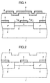
- the first embodiment is a field-effect transistor comprising a gallium-arsenide (GaAs) substrate 1, an source n + region 2, a channel 3, a drain n + region 4, a source electrode 5, a gate electrode 6, a drain electrode 7, an insulating layer 8, and a novel covering electrode 9.
- GaAs gallium-arsenide
- the distance L sg from the source region 2 to the gate electrode 6 and the distance L gd from the gate electrode 6 to the drain region 4 are both equal to one micrometer (1 ⁇ m).
- the insulating layer 8 in FIG. 1 is a silicon-nitride (SiN) layer approximately one thousand angstroms (1000 ⁇ ) thick.
- the novel covering electrode 9 is a patterned metal film comprising titanium, platinum, gold, or an alloy thereof. The covering electrode 9 overlies the entire channel 3 and extends even farther, from a point over the source electrode 5 to a point over the drain electrode 7.
- the gate electrode 6 and covering electrode 9 have respective contact points (not shown) for connection to an external control circuit (not shown), which can apply a gate voltage V g to the gate electrode 6, and a control voltage V c to the covering electrode 9.
- the source and drain electrodes 5 and 7 also have contact points (not shown) for connection to external circuits.
- a positive control voltage V c is also applied to the covering electrode 9.
- the electric field created by the positive voltages at the gate electrode 6 and covering electrode 9 draws carriers (in this case electrons) into the channel 3, so that current can flow between the source and drain regions 2 and 4.
- the gate electrode 6 and covering electrode 9 are internally interconnected, and the external control circuit applies a single gate voltage V g to both electrodes 6 and 9.
- FIG. 2 shows a conventional field-effect transistor, using the same reference numerals as in FIG. 1. Except for the lack of a covering electrode, the conventional field-effect transistor is identical to the first embodiment. A detailed description of the individual elements of the conventional field-effect transistor in FIG. 2, and of the corresponding elements in FIG. 1, will be omitted.
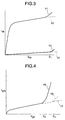
- FIG. 3 illustrates the relationship between source-drain voltage (V ds ), shown on the horizontal axis, and source-drain current (I ds ), shown on the vertical axis, in the symmetric transistors of FIGs. 1 and 2.
- Solid line 11 characterizes the conventional transistor (FIG. 2) in the on-state.
- Dotted line 12 characterizes the first embodiment (FIG. 1) in the on-state, with the same positive voltage applied to both the gate electrode 6 and covering electrode 9. The on-resistance of the transistors can be determined from these characteristics 11 and 12.
- Solid line 13 characterizes the conventional transistor in the off-state.
- Dotted line 14 characterizes the first embodiment in the off-state, with a control voltage V c of minus ten volts (-10 V) applied to the covering electrode 9.
- V c minus ten volts
- the source-drain voltage-current characteristics of the conventional transistor and the first embodiment are identical up to a certain voltage V 1 , at which point the conventional transistor begins to experience source-drain breakdown.
- the breakdown leads to a sharp rise in off-state leakage current in the conventional field-effect transistor.
- the first embodiment continues to maintain good source-drain isolation even above voltage V 1 , allowing only a small leakage current to pass.
- FIG. 4 illustrates the relation between gate-drain voltage (V gd ), shown on the horizontal axis, and gate-drain reverse current (I gdo ), shown on the vertical axis, for the transistors of FIGs. 1 and 2 when the source electrode 5 is left open (not connected).
- Solid line 15 characterizes the conventional transistor.
- Dotted line 16 characterizes the first embodiment when a control voltage V c of -3 V is applied to the covering electrode 9.
- Dash-dot line 17 characterizes the first embodiment when V c is -10 V.
- gate-drain breakdown occurs at voltage V 2 .
- V c is -3 V
- V c gate-drain breakdown does not occur until the higher voltage V 3 is reached, and the breakdown is less severe.
- V c is -10 V breakdown does not occur until a still higher voltage (not shown) is reached.
- the covering electrode 9 in the first embodiment can provide a significant improvement in source-drain and gate-drain breakdown characteristics, with no increase in on-resistance below the breakdown point.
- the covering electrode 9 can be internally coupled to the gate electrode 6, as noted above.
- the improvement in breakdown characteristics will then be limited, but the transistor will not require any extra terminals or leads, and can be controlled in exactly the same way as a conventional field-effect transistor.
- the covering electrode 9 enables the first embodiment to satisfy the conflicting requirements of low on-resistance and very high off-resistance.
- FIG. 5 illustrates a second embodiment of the invented field-effect transistor, using the same reference numerals as in FIG. 1 except for the covering electrode.
- the difference between the first and second embodiments is that the covering electrode 18 in the second embodiment extends only from a point over the gate electrode 6 to a point over the drain electrode 7, thus overlying only that part of the channel 3 disposed between the gate electrode 6 and drain 4.
- the covering electrode 18 may be either independently connected to an external control circuit, or internally connected to the gate electrode 6.
- the covering electrode 18 covers only part of the area from the gate electrode 6 to the drain electrode 7.
- the second embodiment provides improved breakdown characteristics similar to those in the first embodiment.
- the same improvement in gate-drain breakdown voltage is achieved as in the first embodiment.
- the covering electrode 18 since no part of the covering electrode 18 is disposed directly over the source n + region 2 or source electrode 5, capacitive coupling between the source and covering electrode is greatly reduced.
- the transistor conducts very little direct current in the off-state, alternating current is weakly coupled from the drain electrode 7 to the source electrode 5, due to unwanted capacitive coupling of the source and drain electrodes 5 and 7 to the covering electrode 9.
- the second embodiment substantially eliminates one part of this capacitive coupling link, thereby improving the isolation of the source electrode 5 from alternating-current waveforms, such as carrier-signal waveforms, that might be applied to the drain electrode 7.
- FIG. 6 illustrates a third embodiment, using the same reference numerals as in FIG. 1.
- the third embodiment is identical to the first embodiment except that the transistor is asymmetric: the distance L gd from the gate electrode 6 to the drain 4 exceeds the distance L sg from the source 2 to the gate electrode 6.
- L sg is 1 ⁇ m and L gd is 2 ⁇ m.
- the covering electrode 9 can either receive an independent control voltage V c , or be coupled internally to the gate electrode 6 and receive the gate voltage V g .
- the increased distance L gd in the third embodiment increases the length of the channel 3, leading to a somewhat increased on-resistance, but also increases the breakdown voltages in the off-state. Specifically, the doubling of L gd in the third embodiment produces substantially a 33% increase in on-resistance, but a 20% improvement (increase) in the source-drain breakdown voltage, and a 40& improvement (increase) in the gate-drain breakdown voltage.
- FIG. 7 illustrates a fourth embodiment, using the same reference numerals as in FIG. 5.
- the fourth embodiment is identical to the second embodiment except that, as in the third embodiment, L gd exceeds L sg .
- the fourth embodiment combines the advantages of the second and third embodiments: reduced capacitive coupling between the source and drain, and improved source-drain and gate-drain breakdown characteristics.
- the fourth embodiment thus provides excellent alternating-current and direct-current isolation performance in the off-state, with only a slightly increased resistance in the on-state.
- This embodiment couples an antenna to the transmitting and receiving circuits of a device such as a portable telephone set.
- the antenna switch 20 comprises a bridge network of four field-effect transistors Q 1 to Q 4 .
- the letters S and D identify the source and drain of each transistor.
- Transistors Q 1 and Q 4 have the asymmetric structure of the fourth embodiment.
- Transistors Q 2 and Q 3 are conventional symmetric field-effect transistors of the type shown in FIG. 2, without covering electrodes.
- the antenna 21 is coupled to the drain electrodes of transistors Q 1 and Q 2 .
- the receiving circuit (RX) 22 is coupled to the source electrode of transistor Q 1 and to the drain electrode of transistor Q 3 .
- the transmitting circuit (TX) 23 is coupled to the source electrode of transistor Q 2 and to the drain electrode of transistor Q 4 .
- the source electrodes of transistors Q 3 and Q 4 are coupled to a ground terminal 24.
- the control circuit coupled to the gate and covering electrodes of the transistors has been omitted to avoid obscuring the invention with irrelevant detail.
- FIGs. 9 and 10 are network diagrams illustrating the operation of the invented antenna switch.
- transistors Q 1 and Q 4 are switched on, as indicated by solid lines in FIG. 9, while transistors Q 2 and Q 3 are switched off, as indicated by dashed lines.
- the slightly increased on-resistance of transistor Q 1 presents no problem in this state, because the receiving circuit 22 itself has a much higher input impedance.
- the slightly increased on-resistance of transistor Q 4 presents no problem either, because the transmitting circuit 23 is switched off in the receiving state.
- the signal received at the antenna 21 is of course a low-voltage signal, so the conventional breakdown characteristics of transistors Q 2 and Q 3 are adequate to prevent leakage of received signal power to the transmitting circuit 23 or ground terminal 24.
- transistors Q 2 and Q 3 are switched on, as indicated by solid lines in FIG. 10, while transistors Q 1 and Q 4 are switched off, as indicated by dashed lines.
- the strong, high-frequency carrier signal output by the transmitting circuit 23 is coupled with little loss to the antenna 21, because of the low on-resistance of the conventional transistor Q 2 .
- Coupling of this power to the receiving circuit 22 or ground is blocked by the novel transistors Q 1 and Q 4 .
- Direct-current coupling is blocked because of the high source-drain breakdown voltages of these transistors, while capacitive coupling is blocked because their covering electrodes cover only the area between the gate electrode and drain, substantially eliminating capacitive coupling to the source electrode. Thus very little transmitting power is lost in the antenna switch 20.
- the receiving circuit 22 is coupled to the ground terminal 24 through transistor Q 3 . Since the on-resistance of transistor Q 3 is much lower than the input impedance of the receiving circuit 22, the very small amount of transmitting power that leaks through transistor Q 1 is shunted almost entirely to ground; substantially none of the leaking power enters the receiving circuit 22.
- the invented antenna switch 20 is able to combine a low antenna insertion-loss characteristic with excellent isolation of the receiving circuit 22 from the transmitting circuit 23.
- the present invention has been described in relation to an antenna switching circuit, but can be practiced in numerous other circuits as well.
- the invented field-effect transistors can be applied in any type of circuit requiring enhanced isolation performance, including microwave modulating and demodulating circuits, microwave switches, and inverters that chop direct-current power at microwave frequencies. Very high-frequency operation is possible if the gate length of the transistors is shortened, to raise the cut-off frequency f T .
- the circuit configuration of the switch 20 in FIG. 8 is applicable to double-pole double-throw switches in general, and is not limited to antenna switches.
- the semiconductor substrate of the invented transistors is not limited to gallium arsenide.
- Other compound semiconductor materials such as indium-phosphide (InP) and indium-gallium-arsenide (InGaAs), can be used.
- InP and InGaAs have excellent high-frequency characteristics.
- the invention can also be practiced with a silicon semiconductor substrate, and with p-channel transistors instead of n-channel transistors.
Landscapes
- Engineering & Computer Science (AREA)
- Microelectronics & Electronic Packaging (AREA)
- Power Engineering (AREA)
- Physics & Mathematics (AREA)
- Condensed Matter Physics & Semiconductors (AREA)
- General Physics & Mathematics (AREA)
- Computer Hardware Design (AREA)
- Ceramic Engineering (AREA)
- Computer Networks & Wireless Communication (AREA)
- Signal Processing (AREA)
- Manufacturing & Machinery (AREA)
- Junction Field-Effect Transistors (AREA)
- Semiconductor Integrated Circuits (AREA)
- Metal-Oxide And Bipolar Metal-Oxide Semiconductor Integrated Circuits (AREA)
- Transceivers (AREA)
- Variable-Direction Aerials And Aerial Arrays (AREA)
- Details Of Aerials (AREA)
- Thin Film Transistor (AREA)
- Electronic Switches (AREA)
- Waveguide Switches, Polarizers, And Phase Shifters (AREA)
Abstract
Description
- The present invention relates to a solid-state switch for selectively coupling an antenna to transmitting and receiving circuits, and to a type of field-effect transistor useful in this switch and other switches.
- The antennas of time-division multiple-access (TDMA) digital wireless telephone sets, for example, must be switched rapidly between transmitting and receiving functions. Solid-state switches comprising diodes or transistors are commonly employed, as electromechanical switches would be too slow. In particular, a bridge network of field-effect transistors can be used as an antenna switch. The network acts as a double-pole double-throw (DPDT) switch, coupling the transmitting and receiving circuits alternately to the antenna and to ground.
- To avoid loss of transmitting power, and to provide adequate coupling to ground, the field-effect transistors in such a switch must have a low resistance in the on-state. To prevent leakage of transmitted signals into the receiving circuit, however, the transistors also need to have a very high resistance in the off-state. These are conflicting requirements, since a low on-resistance comes from a short channel, while a high off-resistance normally demands a long channel. To isolate receiving and control circuits from the high power output by the transmitter, the transistors must also have high source-drain and gate-drain breakdown voltages, but this too normally requires a long channel, which is incompatible with a low on-resistance.
- It is accordingly an object of the present invention to provide a solid-state antenna switch that combines low-resistance coupling with good isolation.
- Another object of the invention is to provide a field-effect transistor combining a low on-resistance with a high source-drain breakdown voltage.
- Yet another object is to provide a field-effect transistor combining a low on-resistance with a high gate-drain breakdown voltage.
- The invented field-effect transistor has a semiconductor substrate, source, channel, drain, source electrode, gate electrode, and drain electrode as in conventional field-effect transistors. All of these elements are covered by an insulating layer, also as in conventional field-effect transistors. A covering electrode is formed on the insulating layer, overlying at least part of the channel between the gate electrode and drain. One voltage is applied to the covering electrode when the field-effect transistor is switched on, and another voltage is applied when the field-effect transistor is switched off. The voltage applied in the off-state creates an electric field that hinders current flow in the channel.
- The invented antenna switch has a first field-effect transistor that couples an antenna to a receiving circuit, and a second field-effect transistor that couples the antenna to a transmitting circuit. The first field-effect transistor is of the invented type.
- In the attached drawings:
- FIG. 1 is a sectional view of a first embodiment of the invented field-effect transistor;
- FIG. 2 is a sectional view of a conventional field-effect transistor;
- FIG. 3 illustrates source-drain current-voltage characteristics of the invented and conventional field-effect transistors;
- FIG. 4 illustrates gate-drain current-voltage characteristics of the invented and conventional field-effect transistors;
- FIG. 5 is a sectional view of a second embodiment of the invented field-effect transistor;
- FIG. 6 is a sectional view of a third embodiment of the invented field-effect transistor;
- FIG. 7 is a sectional view of a fourth embodiment of the invented field-effect transistor;
- FIG. 8 is a schematic diagram of an embodiment of the invented antenna switch;
- FIG. 9 shows the antenna switch in the receiving state; and
- FIG. 10 shows the antenna switch in the transmitting state.
- Embodiments of the invention will be described below with reference to the drawings. Embodiments of the invented field-effect transistor will be described first, followed by an embodiment of the invented antenna switch.
- Referring to FIG. 1, the first embodiment is a field-effect transistor comprising a gallium-arsenide (GaAs)
substrate 1, an source n+ region 2, achannel 3, a drain n+ region 4, asource electrode 5, agate electrode 6, adrain electrode 7, aninsulating layer 8, and anovel covering electrode 9. The distance Lsg from thesource region 2 to thegate electrode 6 and the distance Lgd from thegate electrode 6 to thedrain region 4 are both equal to one micrometer (1 µm). - The
insulating layer 8 in FIG. 1 is a silicon-nitride (SiN) layer approximately one thousand angstroms (1000 Å) thick. Thenovel covering electrode 9 is a patterned metal film comprising titanium, platinum, gold, or an alloy thereof. The coveringelectrode 9 overlies theentire channel 3 and extends even farther, from a point over thesource electrode 5 to a point over thedrain electrode 7. - The
gate electrode 6 and coveringelectrode 9 have respective contact points (not shown) for connection to an external control circuit (not shown), which can apply a gate voltage Vg to thegate electrode 6, and a control voltage Vc to thecovering electrode 9. The source anddrain electrodes - When the transistor is switched on by application of a positive gate voltage Vg, a positive control voltage Vc is also applied to the
covering electrode 9. The electric field created by the positive voltages at thegate electrode 6 and coveringelectrode 9 draws carriers (in this case electrons) into thechannel 3, so that current can flow between the source anddrain regions - When the transistor is switched off by application of a ground voltage or negative voltage to the
gate electrode 6, a negative control voltage Vc is applied to thecovering electrode 9. The electric field created by the negative control voltage Vc drives carriers (electrons) out of thechannel 3, thus hindering the flow of current between the source anddrain regions - In a variation of the first embodiment, the
gate electrode 6 and coveringelectrode 9 are internally interconnected, and the external control circuit applies a single gate voltage Vg to bothelectrodes - For comparison, FIG. 2 shows a conventional field-effect transistor, using the same reference numerals as in FIG. 1. Except for the lack of a covering electrode, the conventional field-effect transistor is identical to the first embodiment. A detailed description of the individual elements of the conventional field-effect transistor in FIG. 2, and of the corresponding elements in FIG. 1, will be omitted.
- The symmetry of the transistor in FIG. 1 makes the two n+ regions 2 and 4 interchangeable: either
region - FIG. 3 illustrates the relationship between source-drain voltage (Vds), shown on the horizontal axis, and source-drain current (Ids), shown on the vertical axis, in the symmetric transistors of FIGs. 1 and 2.
-
Solid line 11 characterizes the conventional transistor (FIG. 2) in the on-state. Dottedline 12 characterizes the first embodiment (FIG. 1) in the on-state, with the same positive voltage applied to both thegate electrode 6 and coveringelectrode 9. The on-resistance of the transistors can be determined from thesecharacteristics -
Solid line 13 characterizes the conventional transistor in the off-state. Dottedline 14 characterizes the first embodiment in the off-state, with a control voltage Vc of minus ten volts (-10 V) applied to thecovering electrode 9. The off-state characteristics - As FIG. 3 shows, the source-drain voltage-current characteristics of the conventional transistor and the first embodiment are identical up to a certain voltage V1, at which point the conventional transistor begins to experience source-drain breakdown. The breakdown leads to a sharp rise in off-state leakage current in the conventional field-effect transistor. The first embodiment continues to maintain good source-drain isolation even above voltage V1, allowing only a small leakage current to pass.
- FIG. 4 illustrates the relation between gate-drain voltage (Vgd), shown on the horizontal axis, and gate-drain reverse current (Igdo), shown on the vertical axis, for the transistors of FIGs. 1 and 2 when the
source electrode 5 is left open (not connected).Solid line 15 characterizes the conventional transistor.Dotted line 16 characterizes the first embodiment when a control voltage Vc of -3 V is applied to the coveringelectrode 9. Dash-dot line 17 characterizes the first embodiment when Vc is -10 V. In the conventional transistor, gate-drain breakdown occurs at voltage V2. In the first embodiment, when Vc is -3 V, gate-drain breakdown does not occur until the higher voltage V3 is reached, and the breakdown is less severe. When Vc is -10 V, breakdown does not occur until a still higher voltage (not shown) is reached. - As FIGs. 3 and 4 indicate, the covering
electrode 9 in the first embodiment can provide a significant improvement in source-drain and gate-drain breakdown characteristics, with no increase in on-resistance below the breakdown point. - If applying a separate control voltage Vc to the covering
electrode 9 is inconvenient, the coveringelectrode 9 can be internally coupled to thegate electrode 6, as noted above. The improvement in breakdown characteristics will then be limited, but the transistor will not require any extra terminals or leads, and can be controlled in exactly the same way as a conventional field-effect transistor. - In either case, the covering
electrode 9 enables the first embodiment to satisfy the conflicting requirements of low on-resistance and very high off-resistance. - FIG. 5 illustrates a second embodiment of the invented field-effect transistor, using the same reference numerals as in FIG. 1 except for the covering electrode. The difference between the first and second embodiments is that the covering
electrode 18 in the second embodiment extends only from a point over thegate electrode 6 to a point over thedrain electrode 7, thus overlying only that part of thechannel 3 disposed between thegate electrode 6 anddrain 4. As in the first embodiment, the coveringelectrode 18 may be either independently connected to an external control circuit, or internally connected to thegate electrode 6. - In a variation of the second embodiment, the covering
electrode 18 covers only part of the area from thegate electrode 6 to thedrain electrode 7. - The second embodiment provides improved breakdown characteristics similar to those in the first embodiment. In particular, the same improvement in gate-drain breakdown voltage is achieved as in the first embodiment. In addition, since no part of the covering
electrode 18 is disposed directly over the source n+ region 2 orsource electrode 5, capacitive coupling between the source and covering electrode is greatly reduced. - In the first embodiment, although the transistor conducts very little direct current in the off-state, alternating current is weakly coupled from the
drain electrode 7 to thesource electrode 5, due to unwanted capacitive coupling of the source anddrain electrodes electrode 9. The second embodiment substantially eliminates one part of this capacitive coupling link, thereby improving the isolation of thesource electrode 5 from alternating-current waveforms, such as carrier-signal waveforms, that might be applied to thedrain electrode 7. - FIG. 6 illustrates a third embodiment, using the same reference numerals as in FIG. 1. The third embodiment is identical to the first embodiment except that the transistor is asymmetric: the distance Lgd from the
gate electrode 6 to thedrain 4 exceeds the distance Lsg from thesource 2 to thegate electrode 6. Specifically, Lsg is 1 µm and Lgd is 2 µm. As in the first embodiment, the coveringelectrode 9 can either receive an independent control voltage Vc, or be coupled internally to thegate electrode 6 and receive the gate voltage Vg. - The increased distance Lgd in the third embodiment increases the length of the
channel 3, leading to a somewhat increased on-resistance, but also increases the breakdown voltages in the off-state. Specifically, the doubling of Lgd in the third embodiment produces substantially a 33% increase in on-resistance, but a 20% improvement (increase) in the source-drain breakdown voltage, and a 40& improvement (increase) in the gate-drain breakdown voltage. - FIG. 7 illustrates a fourth embodiment, using the same reference numerals as in FIG. 5. The fourth embodiment is identical to the second embodiment except that, as in the third embodiment, Lgd exceeds Lsg. The fourth embodiment combines the advantages of the second and third embodiments: reduced capacitive coupling between the source and drain, and improved source-drain and gate-drain breakdown characteristics. The fourth embodiment thus provides excellent alternating-current and direct-current isolation performance in the off-state, with only a slightly increased resistance in the on-state.
- Next, an embodiment of the invented antenna switch will be described. This embodiment couples an antenna to the transmitting and receiving circuits of a device such as a portable telephone set.
- Referring to FIG. 8, the
antenna switch 20 comprises a bridge network of four field-effect transistors Q1 to Q4. The letters S and D identify the source and drain of each transistor. Transistors Q1 and Q4 have the asymmetric structure of the fourth embodiment. Transistors Q2 and Q3 are conventional symmetric field-effect transistors of the type shown in FIG. 2, without covering electrodes. - The
antenna 21 is coupled to the drain electrodes of transistors Q1 and Q2. The receiving circuit (RX) 22 is coupled to the source electrode of transistor Q1 and to the drain electrode of transistor Q3. The transmitting circuit (TX) 23 is coupled to the source electrode of transistor Q2 and to the drain electrode of transistor Q4. The source electrodes of transistors Q3 and Q4 are coupled to aground terminal 24. The control circuit coupled to the gate and covering electrodes of the transistors has been omitted to avoid obscuring the invention with irrelevant detail. - FIGs. 9 and 10 are network diagrams illustrating the operation of the invented antenna switch.
- In the receiving state, transistors Q1 and Q4 are switched on, as indicated by solid lines in FIG. 9, while transistors Q2 and Q3 are switched off, as indicated by dashed lines. The slightly increased on-resistance of transistor Q1 presents no problem in this state, because the receiving
circuit 22 itself has a much higher input impedance. The slightly increased on-resistance of transistor Q4 presents no problem either, because the transmittingcircuit 23 is switched off in the receiving state. The signal received at theantenna 21 is of course a low-voltage signal, so the conventional breakdown characteristics of transistors Q2 and Q3 are adequate to prevent leakage of received signal power to the transmittingcircuit 23 orground terminal 24. - In the transmitting state, transistors Q2 and Q3 are switched on, as indicated by solid lines in FIG. 10, while transistors Q1 and Q4 are switched off, as indicated by dashed lines. The strong, high-frequency carrier signal output by the transmitting
circuit 23 is coupled with little loss to theantenna 21, because of the low on-resistance of the conventional transistor Q2. Coupling of this power to the receivingcircuit 22 or ground is blocked by the novel transistors Q1 and Q4. Direct-current coupling is blocked because of the high source-drain breakdown voltages of these transistors, while capacitive coupling is blocked because their covering electrodes cover only the area between the gate electrode and drain, substantially eliminating capacitive coupling to the source electrode. Thus very little transmitting power is lost in theantenna switch 20. - In addition, in the transmitting state, the receiving
circuit 22 is coupled to theground terminal 24 through transistor Q3. Since the on-resistance of transistor Q3 is much lower than the input impedance of the receivingcircuit 22, the very small amount of transmitting power that leaks through transistor Q1 is shunted almost entirely to ground; substantially none of the leaking power enters the receivingcircuit 22. - By employing both field-effect transistors of the conventional symmetric type and novel transistors of the asymmetric type with covering electrodes, the invented
antenna switch 20 is able to combine a low antenna insertion-loss characteristic with excellent isolation of the receivingcircuit 22 from the transmittingcircuit 23. - The present invention has been described in relation to an antenna switching circuit, but can be practiced in numerous other circuits as well.
- The invented field-effect transistors can be applied in any type of circuit requiring enhanced isolation performance, including microwave modulating and demodulating circuits, microwave switches, and inverters that chop direct-current power at microwave frequencies. Very high-frequency operation is possible if the gate length of the transistors is shortened, to raise the cut-off frequency fT.
- The circuit configuration of the
switch 20 in FIG. 8 is applicable to double-pole double-throw switches in general, and is not limited to antenna switches. - The semiconductor substrate of the invented transistors is not limited to gallium arsenide. Other compound semiconductor materials, such as indium-phosphide (InP) and indium-gallium-arsenide (InGaAs), can be used. (InP and InGaAs have excellent high-frequency characteristics.) The invention can also be practiced with a silicon semiconductor substrate, and with p-channel transistors instead of n-channel transistors.
- Those skilled in the art will recognize that other variations are possible.
Claims (16)
- A field-effect transistor having a semiconductor substrate (1), a source (2) and a drain (4) formed in the semiconductor substrate, a channel (3) for conducting current in the semiconductor substrate between the source and the drain, a gate electrode (6) formed on the semiconductor substrate above part of the channel, for controlling said current, and an insulating layer (8) covering the semiconductor substrate and the gate electrode, also comprising:a covering electrode (9) formed on said insulating layer, overlying at least part of said channel, for receiving one voltage when said field-effect transistor is switched on and another voltage when said field-effect transistor is switched off, said other voltage creating an electric field that hinders current flow in said channel.
- The field-effect transistor of claim 1, wherein said gate electrode (6) and said covering electrode (9) receive independent voltages.
- The field-effect transistor of claim 1, wherein said covering electrode (9) is coupled to said gate electrode (6).
- The field-effect transistor of claim 1, wherein said source (2) and said drain (4) are equidistant from said gate electrode (6).
- The field-effect transistor of claim 4, wherein said covering electrode (9) overlies all of said channel (3).
- The field-effect transistor of claim 4, wherein said covering electrode (9) overlies at least part of said channel (3) disposed between said gate electrode (6) and said drain (4), and does not overlie any part of said channel disposed between said source (2) and said gate electrode.
- The field-effect transistor of claim 1, wherein said gate electrode (6) is farther from said drain (4) than from said source (2).
- The field-effect transistor of claim 7, wherein said covering electrode (9) overlies all of said channel (3).
- The field-effect transistor of claim 7, wherein said covering electrode (9) overlies at least part of said channel (3) disposed between said gate electrode (6) and said drain (4), and does not overlie any part of said channel disposed between said source (2) and said gate electrode.
- An antenna switching circuit having a first field-effect transistor (Q1) coupling an antenna (21) to a receiving circuit (22), and a second field-effect transistor (Q2) coupling said antenna to a transmitting circuit (23), wherein said first field-effect transistor has:a semiconductor substrate (1) with a source (2) coupled to said receiving circuit, a drain (4) coupled to said antenna, and a channel (3) for conducting current between said source and said drain;a gate electrode (6) formed on said semiconductor substrate, covering part of said channel, for controlling said current;an insulating layer (8) formed on said semiconductor substrate, covering said semiconductor substrate and said gate electrode; anda covering electrode (9) formed on said insulating layer, overlying at least part of said channel between said gate electrode and said drain, for receiving one voltage when said field-effect transistor is switched on and another voltage when said field-effect transistor is switched off, said other voltage creating an electric field that hinders current flow in said channel.
- The antenna switching circuit of claim 10 wherein, in said first field-effect transistor (Q1), said gate electrode (6) is farther from said drain (4) than from said source (2).
- The antenna switching circuit of claim 10 wherein, in said first field-effect transistor (Q1), said covering electrode (9) does not overlie any part of said channel (3) between said source (2) and said gate electrode (6).
- The antenna switching circuit of claim 10, wherein said second field-effect transistor (Q2) is symmetric.
- The antenna switching circuit of claim 10, also comprising:a ground terminal (24);a third field-effect transistor (Q3) coupling said receiving circuit to said ground terminal, said third field-effect transistor being switched on and off simultaneously with said second field-effect transistor (Q2); anda fourth field-effect transistor (Q4) coupling said transmitting circuit to said ground terminal, said fourth field-effect transistor being switched on and off simultaneously with said first field-effect transistor (Q1).
- The antenna switching circuit of claim 14, wherein said third field-effect transistor is symmetric.
- The antenna switching circuit of claim 14, wherein said fourth field-effect transistor has a covering electrode similar to the covering electrode of said first field-effect transistor.
Applications Claiming Priority (3)
| Application Number | Priority Date | Filing Date | Title |
|---|---|---|---|
| JP8033221A JPH09232827A (en) | 1996-02-21 | 1996-02-21 | Semiconductor device and transmission/reception changeover antenna switch circuit |
| JP3322196 | 1996-02-21 | ||
| JP33221/96 | 1996-02-21 |
Publications (2)
| Publication Number | Publication Date |
|---|---|
| EP0792028A2 true EP0792028A2 (en) | 1997-08-27 |
| EP0792028A3 EP0792028A3 (en) | 2001-12-12 |
Family
ID=12380401
Family Applications (1)
| Application Number | Title | Priority Date | Filing Date |
|---|---|---|---|
| EP97101898A Withdrawn EP0792028A3 (en) | 1996-02-21 | 1997-02-06 | Solid-state antenna switch and field-effect transistor |
Country Status (5)
| Country | Link |
|---|---|
| US (1) | US5872369A (en) |
| EP (1) | EP0792028A3 (en) |
| JP (1) | JPH09232827A (en) |
| KR (1) | KR100325087B1 (en) |
| CN (1) | CN1113417C (en) |
Cited By (15)
| Publication number | Priority date | Publication date | Assignee | Title |
|---|---|---|---|---|
| EP1326283A2 (en) * | 2002-01-08 | 2003-07-09 | NEC Compound Semiconductor Devices, Ltd. | Schottky gate field effect transistor |
| EP1363331A2 (en) * | 2002-04-17 | 2003-11-19 | Sanyo Electric Co., Ltd. | Semiconductor switching circuit device and manufacturing method thereof |
| EP1376694A2 (en) * | 2002-04-17 | 2004-01-02 | Sanyo Electric Co., Ltd. | Semiconductor switching circuit device |
| WO2006098801A1 (en) | 2005-03-11 | 2006-09-21 | Cree, Inc. | Wide bandgap transistors with gate-source field plates |
| US7501669B2 (en) | 2003-09-09 | 2009-03-10 | Cree, Inc. | Wide bandgap transistor devices with field plates |
| US7550783B2 (en) | 2004-05-11 | 2009-06-23 | Cree, Inc. | Wide bandgap HEMTs with source connected field plates |
| US7573078B2 (en) | 2004-05-11 | 2009-08-11 | Cree, Inc. | Wide bandgap transistors with multiple field plates |
| US7692263B2 (en) | 2006-11-21 | 2010-04-06 | Cree, Inc. | High voltage GaN transistors |
| US7709269B2 (en) | 2006-01-17 | 2010-05-04 | Cree, Inc. | Methods of fabricating transistors including dielectrically-supported gate electrodes |
| US7960756B2 (en) | 2006-01-17 | 2011-06-14 | Cree, Inc. | Transistors including supported gate electrodes |
| US8283699B2 (en) | 2006-11-13 | 2012-10-09 | Cree, Inc. | GaN based HEMTs with buried field plates |
| US8823057B2 (en) | 2006-11-06 | 2014-09-02 | Cree, Inc. | Semiconductor devices including implanted regions for providing low-resistance contact to buried layers and related devices |
| US9679981B2 (en) | 2013-06-09 | 2017-06-13 | Cree, Inc. | Cascode structures for GaN HEMTs |
| US9773877B2 (en) | 2004-05-13 | 2017-09-26 | Cree, Inc. | Wide bandgap field effect transistors with source connected field plates |
| US9847411B2 (en) | 2013-06-09 | 2017-12-19 | Cree, Inc. | Recessed field plate transistor structures |
Families Citing this family (19)
| Publication number | Priority date | Publication date | Assignee | Title |
|---|---|---|---|---|
| JP3111985B2 (en) * | 1998-06-16 | 2000-11-27 | 日本電気株式会社 | Field-effect transistor |
| JP3180776B2 (en) * | 1998-09-22 | 2001-06-25 | 日本電気株式会社 | Field-effect transistor |
| US6882829B2 (en) * | 2002-04-02 | 2005-04-19 | Texas Instruments Incorporated | Integrated circuit incorporating RF antenna switch and power amplifier |
| JP2004006816A (en) * | 2002-04-17 | 2004-01-08 | Sanyo Electric Co Ltd | Semiconductor switch circuit device and its manufacture |
| TWI430341B (en) * | 2003-09-09 | 2014-03-11 | Univ California | Fabrication of single or multiple gate field plates |
| KR100592735B1 (en) * | 2004-11-16 | 2006-06-26 | 한국전자통신연구원 | Transistor of semiconductor element and a method for fabricating the same |
| JP2006173571A (en) * | 2004-12-14 | 2006-06-29 | Korea Electronics Telecommun | Transistor of semiconductor device and method of manufacturing the transistor |
| JP2006202948A (en) * | 2005-01-20 | 2006-08-03 | Toshiba Corp | Semiconductor device |
| JP4870644B2 (en) * | 2006-12-05 | 2012-02-08 | 韓國電子通信研究院 | High isolation switch element for millimeter wave band control circuit |
| KR100976627B1 (en) * | 2007-12-10 | 2010-08-18 | 한국전자통신연구원 | Switching circuit for millimeter wave band applications |
| JP5691267B2 (en) * | 2010-07-06 | 2015-04-01 | サンケン電気株式会社 | Semiconductor device |
| JP5735268B2 (en) * | 2010-12-20 | 2015-06-17 | サムソン エレクトロ−メカニックス カンパニーリミテッド. | High frequency semiconductor switch |
| CN103219977B (en) * | 2012-01-19 | 2016-08-24 | 三星电机株式会社 | high-frequency semiconductor switch |
| JP2013182992A (en) * | 2012-03-01 | 2013-09-12 | Toshiba Corp | Semiconductor device |
| JP2013183062A (en) * | 2012-03-02 | 2013-09-12 | Toshiba Corp | Semiconductor device |
| JP2014017423A (en) * | 2012-07-10 | 2014-01-30 | Fujitsu Ltd | Compound semiconductor device and method for manufacturing the same |
| US10014475B2 (en) | 2013-04-17 | 2018-07-03 | Empire Technology Development Llc | Graphene nanoribbons as semiconductors for organic thin film transistors |
| US9755059B2 (en) | 2013-06-09 | 2017-09-05 | Cree, Inc. | Cascode structures with GaN cap layers |
| US9425308B2 (en) * | 2013-12-31 | 2016-08-23 | Delta Electronics, Inc. | Power semiconductor device and method for fabricating the same |
Citations (3)
| Publication number | Priority date | Publication date | Assignee | Title |
|---|---|---|---|---|
| US4757362A (en) * | 1980-05-30 | 1988-07-12 | Sharp Kabushiki Kaisha | High voltage MOS transistor |
| US4947232A (en) * | 1980-03-22 | 1990-08-07 | Sharp Kabushiki Kaisha | High voltage MOS transistor |
| EP0409374A2 (en) * | 1989-07-18 | 1991-01-23 | Mitsubishi Denki Kabushiki Kaisha | A Microwave or Millimetre Wave Circuit |
Family Cites Families (8)
| Publication number | Priority date | Publication date | Assignee | Title |
|---|---|---|---|---|
| USRE32369E (en) * | 1980-11-17 | 1987-03-10 | Ball Corporation | Monolithic microwave integrated circuit with integral array antenna |
| JPS6177359A (en) * | 1984-09-21 | 1986-04-19 | Fujitsu Ltd | Semiconductor memory device |
| US4894114A (en) * | 1987-02-11 | 1990-01-16 | Westinghouse Electric Corp. | Process for producing vias in semiconductor |
| US5585288A (en) * | 1990-07-16 | 1996-12-17 | Raytheon Company | Digital MMIC/analog MMIC structures and process |
| US5705940A (en) * | 1990-07-16 | 1998-01-06 | Raytheon Company | Logic family for digitally controlled analog monolithic microwave integrated circuits |
| JPH05243572A (en) * | 1992-02-27 | 1993-09-21 | Fujitsu Ltd | Semiconductor device |
| JPH0799251A (en) * | 1992-12-10 | 1995-04-11 | Sony Corp | Semiconductor memory cell |
| JP2738315B2 (en) * | 1994-11-22 | 1998-04-08 | 日本電気株式会社 | Thin film transistor and method of manufacturing the same |
-
1996
- 1996-02-21 JP JP8033221A patent/JPH09232827A/en not_active Abandoned
-
1997
- 1997-01-30 US US08/791,845 patent/US5872369A/en not_active Expired - Fee Related
- 1997-02-05 KR KR1019970003625A patent/KR100325087B1/en not_active IP Right Cessation
- 1997-02-06 EP EP97101898A patent/EP0792028A3/en not_active Withdrawn
- 1997-02-21 CN CN97102822A patent/CN1113417C/en not_active Expired - Fee Related
Patent Citations (3)
| Publication number | Priority date | Publication date | Assignee | Title |
|---|---|---|---|---|
| US4947232A (en) * | 1980-03-22 | 1990-08-07 | Sharp Kabushiki Kaisha | High voltage MOS transistor |
| US4757362A (en) * | 1980-05-30 | 1988-07-12 | Sharp Kabushiki Kaisha | High voltage MOS transistor |
| EP0409374A2 (en) * | 1989-07-18 | 1991-01-23 | Mitsubishi Denki Kabushiki Kaisha | A Microwave or Millimetre Wave Circuit |
Non-Patent Citations (2)
| Title |
|---|
| KOHAMA K ET AL: "HIGH POWER DPDT ANTENNA SWITCH MMIC FOR DIGITAL CELLULAR SYSTEMS" IEEE GALLIUM ARSENIDE INTEGRATED CIRCUITS (GAAS IC) SYMPOSIUM. 17TH. ANNUAL TECHNICAL DIGEST 1995. SAN DIEGO, OCT. 29 - NOV. 1, 1995, NEW YORK, IEEE, US, vol. SYMP. 17, 29 October 1995 (1995-10-29), pages 75-78, XP000630154 ISBN: 0-7803-2967-8 * |
| UDA H ET AL: "HIGH-PERFORMANCE GAAS SWITCH ICS FABRICATED USING MESFETS WITH TWO KINDS OF PINCH-OFF VOLTAGES" PROCEEDINGS OF THE GALLIUM ARSENIDE INTEGRATED CIRCUITS SYMPOSIUM. (GAAS IC). SAN JOSE, OCT. 10 - 13, 1993, NEW YORK, IEEE, US, vol. SYMP. 15, 10 October 1993 (1993-10-10), pages 247-250, XP000462982 * |
Cited By (33)
| Publication number | Priority date | Publication date | Assignee | Title |
|---|---|---|---|---|
| EP1326283A2 (en) * | 2002-01-08 | 2003-07-09 | NEC Compound Semiconductor Devices, Ltd. | Schottky gate field effect transistor |
| EP1326283A3 (en) * | 2002-01-08 | 2004-01-02 | NEC Compound Semiconductor Devices, Ltd. | Schottky gate field effect transistor |
| US6717192B2 (en) | 2002-01-08 | 2004-04-06 | Nec Compound Semiconductor Devices, Ltd. | Schottky gate field effect transistor |
| EP1363331A2 (en) * | 2002-04-17 | 2003-11-19 | Sanyo Electric Co., Ltd. | Semiconductor switching circuit device and manufacturing method thereof |
| EP1376694A2 (en) * | 2002-04-17 | 2004-01-02 | Sanyo Electric Co., Ltd. | Semiconductor switching circuit device |
| EP1363331A3 (en) * | 2002-04-17 | 2006-05-17 | Sanyo Electric Co., Ltd. | Semiconductor switching circuit device and manufacturing method thereof |
| EP1376694A3 (en) * | 2002-04-17 | 2006-08-23 | Sanyo Electric Co., Ltd. | Semiconductor switching circuit device |
| US7501669B2 (en) | 2003-09-09 | 2009-03-10 | Cree, Inc. | Wide bandgap transistor devices with field plates |
| US9397173B2 (en) | 2003-09-09 | 2016-07-19 | Cree, Inc. | Wide bandgap transistor devices with field plates |
| US7928475B2 (en) | 2003-09-09 | 2011-04-19 | Cree, Inc. | Wide bandgap transistor devices with field plates |
| US8120064B2 (en) | 2003-09-09 | 2012-02-21 | Cree, Inc. | Wide bandgap transistor devices with field plates |
| US8592867B2 (en) | 2004-05-11 | 2013-11-26 | Cree, Inc. | Wide bandgap HEMTS with source connected field plates |
| US7550783B2 (en) | 2004-05-11 | 2009-06-23 | Cree, Inc. | Wide bandgap HEMTs with source connected field plates |
| US7573078B2 (en) | 2004-05-11 | 2009-08-11 | Cree, Inc. | Wide bandgap transistors with multiple field plates |
| US7915644B2 (en) | 2004-05-11 | 2011-03-29 | Cree, Inc. | Wide bandgap HEMTs with source connected field plates |
| US8664695B2 (en) | 2004-05-11 | 2014-03-04 | Cree, Inc. | Wide bandgap transistors with multiple field plates |
| US9773877B2 (en) | 2004-05-13 | 2017-09-26 | Cree, Inc. | Wide bandgap field effect transistors with source connected field plates |
| US11791385B2 (en) | 2005-03-11 | 2023-10-17 | Wolfspeed, Inc. | Wide bandgap transistors with gate-source field plates |
| WO2006098801A1 (en) | 2005-03-11 | 2006-09-21 | Cree, Inc. | Wide bandgap transistors with gate-source field plates |
| US7960756B2 (en) | 2006-01-17 | 2011-06-14 | Cree, Inc. | Transistors including supported gate electrodes |
| US8049252B2 (en) | 2006-01-17 | 2011-11-01 | Cree, Inc. | Methods of fabricating transistors including dielectrically-supported gate electrodes and related devices |
| US7709269B2 (en) | 2006-01-17 | 2010-05-04 | Cree, Inc. | Methods of fabricating transistors including dielectrically-supported gate electrodes |
| US8823057B2 (en) | 2006-11-06 | 2014-09-02 | Cree, Inc. | Semiconductor devices including implanted regions for providing low-resistance contact to buried layers and related devices |
| US9984881B2 (en) | 2006-11-06 | 2018-05-29 | Cree, Inc. | Methods of fabricating semiconductor devices including implanted regions for providing low-resistance contact to buried layers and related devices |
| US8283699B2 (en) | 2006-11-13 | 2012-10-09 | Cree, Inc. | GaN based HEMTs with buried field plates |
| US8933486B2 (en) | 2006-11-13 | 2015-01-13 | Cree, Inc. | GaN based HEMTs with buried field plates |
| US9041064B2 (en) | 2006-11-21 | 2015-05-26 | Cree, Inc. | High voltage GaN transistor |
| US7893500B2 (en) | 2006-11-21 | 2011-02-22 | Cree, Inc. | High voltage GaN transistors |
| US9450081B2 (en) | 2006-11-21 | 2016-09-20 | Cree, Inc. | High voltage GaN transistor |
| US8169005B2 (en) | 2006-11-21 | 2012-05-01 | Cree, Inc. | High voltage GaN transistors |
| US7692263B2 (en) | 2006-11-21 | 2010-04-06 | Cree, Inc. | High voltage GaN transistors |
| US9679981B2 (en) | 2013-06-09 | 2017-06-13 | Cree, Inc. | Cascode structures for GaN HEMTs |
| US9847411B2 (en) | 2013-06-09 | 2017-12-19 | Cree, Inc. | Recessed field plate transistor structures |
Also Published As
| Publication number | Publication date |
|---|---|
| KR970063583A (en) | 1997-09-12 |
| US5872369A (en) | 1999-02-16 |
| KR100325087B1 (en) | 2002-09-05 |
| CN1113417C (en) | 2003-07-02 |
| EP0792028A3 (en) | 2001-12-12 |
| JPH09232827A (en) | 1997-09-05 |
| CN1166694A (en) | 1997-12-03 |
Similar Documents
| Publication | Publication Date | Title |
|---|---|---|
| US5872369A (en) | Solid-state antenna switch and field-effect transistor | |
| US5818099A (en) | MOS high frequency switch circuit using a variable well bias | |
| US5313083A (en) | R.F. switching circuits | |
| US20100327948A1 (en) | Switching Circuit | |
| US20010040479A1 (en) | Electronic switch | |
| EP1156530B1 (en) | Compound semiconductor switching device for high frequency switching | |
| US6967517B2 (en) | Switching device | |
| EP1237277A2 (en) | Semiconductor switching device | |
| US4698524A (en) | MESFET logic using integral diode level shifting | |
| EP1265284B1 (en) | Semiconductor switching device | |
| KR100644980B1 (en) | Compound semiconductor switch circuit device | |
| EP0373803A2 (en) | R. F. switching circuits | |
| US6737890B2 (en) | Switching circuit device | |
| EP1246257B1 (en) | Semiconductor switching device | |
| US8299835B2 (en) | Radio-frequency switch circuit with separately controlled shunt switching device | |
| US7012285B2 (en) | Semiconductor device | |
| US6903426B2 (en) | Semiconductor switching device | |
| JP3539106B2 (en) | High frequency semiconductor switch circuit and control method using the same | |
| JP2002261593A (en) | Compound semiconductor switching circuit | |
| CN116232015A (en) | Automatic reverse blocking bidirectional switch | |
| CN100487895C (en) | Compound semiconductor device | |
| JP2001326333A (en) | Compound semiconductor switch circuit device | |
| JP2001015527A (en) | Semiconductor device |
Legal Events
| Date | Code | Title | Description |
|---|---|---|---|
| PUAI | Public reference made under article 153(3) epc to a published international application that has entered the european phase |
Free format text: ORIGINAL CODE: 0009012 |
|
| AK | Designated contracting states |
Kind code of ref document: A2 Designated state(s): DE FR GB |
|
| PUAL | Search report despatched |
Free format text: ORIGINAL CODE: 0009013 |
|
| AK | Designated contracting states |
Kind code of ref document: A3 Designated state(s): DE FR GB |
|
| RIC1 | Information provided on ipc code assigned before grant |
Free format text: 7H 04B 1/48 A, 7H 03K 17/687 B |
|
| 17P | Request for examination filed |
Effective date: 20020510 |
|
| 17Q | First examination report despatched |
Effective date: 20040628 |
|
| STAA | Information on the status of an ep patent application or granted ep patent |
Free format text: STATUS: THE APPLICATION IS DEEMED TO BE WITHDRAWN |
|
| 18D | Application deemed to be withdrawn |
Effective date: 20041109 |