EP0409374A2 - A Microwave or Millimetre Wave Circuit - Google Patents
A Microwave or Millimetre Wave Circuit Download PDFInfo
- Publication number
- EP0409374A2 EP0409374A2 EP90302902A EP90302902A EP0409374A2 EP 0409374 A2 EP0409374 A2 EP 0409374A2 EP 90302902 A EP90302902 A EP 90302902A EP 90302902 A EP90302902 A EP 90302902A EP 0409374 A2 EP0409374 A2 EP 0409374A2
- Authority
- EP
- European Patent Office
- Prior art keywords
- fet
- microwave
- capacitance
- diode
- drain
- Prior art date
- Legal status (The legal status is an assumption and is not a legal conclusion. Google has not performed a legal analysis and makes no representation as to the accuracy of the status listed.)
- Granted
Links
Images


Classifications
-
- H—ELECTRICITY
- H01—ELECTRIC ELEMENTS
- H01P—WAVEGUIDES; RESONATORS, LINES, OR OTHER DEVICES OF THE WAVEGUIDE TYPE
- H01P1/00—Auxiliary devices
- H01P1/18—Phase-shifters
- H01P1/185—Phase-shifters using a diode or a gas filled discharge tube
-
- H—ELECTRICITY
- H01—ELECTRIC ELEMENTS
- H01P—WAVEGUIDES; RESONATORS, LINES, OR OTHER DEVICES OF THE WAVEGUIDE TYPE
- H01P1/00—Auxiliary devices
- H01P1/10—Auxiliary devices for switching or interrupting
- H01P1/15—Auxiliary devices for switching or interrupting by semiconductor devices
-
- H—ELECTRICITY
- H03—ELECTRONIC CIRCUITRY
- H03K—PULSE TECHNIQUE
- H03K17/00—Electronic switching or gating, i.e. not by contact-making and –breaking
- H03K17/14—Modifications for compensating variations of physical values, e.g. of temperature
- H03K17/145—Modifications for compensating variations of physical values, e.g. of temperature in field-effect transistor switches
-
- H—ELECTRICITY
- H03—ELECTRONIC CIRCUITRY
- H03K—PULSE TECHNIQUE
- H03K17/00—Electronic switching or gating, i.e. not by contact-making and –breaking
- H03K17/51—Electronic switching or gating, i.e. not by contact-making and –breaking characterised by the components used
- H03K17/56—Electronic switching or gating, i.e. not by contact-making and –breaking characterised by the components used by the use, as active elements, of semiconductor devices
- H03K17/687—Electronic switching or gating, i.e. not by contact-making and –breaking characterised by the components used by the use, as active elements, of semiconductor devices the devices being field-effect transistors
- H03K17/693—Switching arrangements with several input- or output-terminals, e.g. multiplexers, distributors
Definitions
- the present invention relates to microwave elements, and more particularly to control circuits utilized in a switch or a phase shifter in microwave or millimeter wave band.
- Figure 4(a) shows a circuit construction of a prior art microwave switch.
- denoted at 1 is an RF input terminal.
- Denoted at 2 and 3 are a first and a second RF terminals, respectively.
- a first and a second FET 6, 7 are connected between the RF input terminal 1 and the RF output terminals 2, 3, respectively.
- Denoted at 4 are gate terminals of the FET 6 and the FET 7, respectively.
- Inductances 5 are connected in parallel with the FET 6 and the FET 7, respectively.
- Figure 4(b) shows an equivalent circuit of an FET in a state where the FET is off and figure 4(c) shows an equivalent circuit in a state where the FET is on.
- This switch operates as follows. In order to make an RF signal input from the input terminal 1 and output from the first output terminal 2, 0v is applied to the gate terminal 4 of the FET 6 thereby to turn on the FET 6. A voltage not exceeding the FET pinch-off voltage, for example, -5 V, is applied to the gate terminal 4 of the FET 7 thereby to turn off the FET 7. Then, the FET 6 and the FET 7 are thought to be equivalent to the circuits of figures 4(c) and 4(b), respectively. Since only a resistance is inserted between the terminals 1 and 2, the RF signal transmits from the terminal 1 to the terminal 2.
- a resonance circuit comprising the inductance 5 connected with the FET 7 and the capacitance of the FET 7 resonates at a desired frequency, and the electrical state thereof becomes similar to a state where infinite impedance is inserted thereat, therefore the RF signal does not transmit from the terminal 1 to the terminal 3.
- the RF signal transmits to the second output terminal 3.
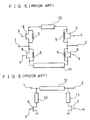
- Figure 5 shows a prior art microwave switched- line type phase shifter.
- the same reference numerals denote the same elements as those shown in figure 4.
- Reference numerals 8 and 9 designate a third and a fourth FET, respectively.
- Denoted at 10 and 11 are a first and a second transmission line, respectively.
- This phase shifter operates as follows. In a case where the FET 6 and the FET 7 are turned on and the FET 8 and the FET 9 are turned off by controlling the voltages applied to the gate terminal 4, the RF signal which is input from the input terminal 1 is output to the output terminal 2 through the first transmission line 10. To the contrary, in a case where the FET 6 and the FET 7 are turned off, and the FET 8 and the FET 9 are turned on, the RF signal input from the input terminal 1 transmits through the second transmission line 11. In these cases, since the transmission lines 10 and 11 have a required length difference, the phase shift amount between the two states can be varied.
- FIG. 6 shows a prior art loaded line type phase shifter.
- the same reference numerals denote the same elements as those shown in figures 4 and 5.
- Denoted at 12 is a third transmission line.
- This loaded line type phase shifter is constructed of a transmission line 12 of a quarter wavelength and two pairs of series connection of transmission line and FET.
- the parameters of the series connection pair of transmission line and FET (a pair of 10 and 6, and that of 11 and 7) are set such that the susceptance value viewed from the main line 12 is -jB in a state where the FETs 6 and 7 are on and that the susceptance value is + jB in a state where the FETs 6 and 7 are off.
- the length of the main line 12 is set to produce such a required difference between the phase of the input signal and that of the output signal of the main line 12.
- the attenuation amount S21 of the output terminal 2 viewed from the input terminal 1 takes the maximum at about 9 GHz, and when it is 0. 15 pF, the attenuation amount S21 takes the maximum at about 11 GHz.
- the resonance frequency at which the impedance becomes infinite varies to a great extent due to the variations in the characteristics of the FET 5.
- a series connection of a diode and a capacitance is loaded in parallel to between the source and the drain of FET, and the bias voltage of the diode is controlled to adjust the capacitance between the source and the drain of FET at off state. Therefore, even when the capacitance of FET at off state varies due to the variations in the FET characteristics, the constant uniform circuit characteristics can be obtained, and the impedance control by FET can be performed at high precision.
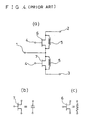
- Figure 1(a) is a diagram showing a circuit construction of a microwave switch according to a first embodiment of the present invention.
- denoted at 1 is an RF input terminal.
- Denoted at 2 and 3 are a first and a second RF output terminals, respectively.
- a first and a second FET 6 and 7 are connected between the RF input terminal 1 and the RF output terminals 2, 3, respectively.
- Denoted at 4 are gate terminals of the FETs 6 and 7.
- Inductances 5 are connected in parallel with the FETs 6 and 7, respectively.
- Serial connections of a capacitor 14 and a diode 15, 16 are connected in parallel with the FET 6 and FET 7, respectively.
- Figures 1(b) and 1(c) are diagrams showing an equivalent circuit of a portion of the microwave switch in a state where the FET is off and on, respectively.
- This microwave switch operates as follows. In order to make an RF signal input to the input terminal 1 and output from the output terminal 2, 0V is applied to the gate terminal 4 of the FET 6 to turn on the FET 6. A voltage not exceeding an FET pinch-off voltage, for example, -5 v, is applied to the gate terminal 4 of the FET 7 thereby to turn off the FET 7. Then the FET 6 and FET 7 are thought to be equivalent to the circuits of figures 1(c) and 1(b), respectively. As in the prior art, since only a resistance is inserted between the terminals 1 and 2 in that state, the RF signal transmits from the input terminal 1 to the first output terminal 2.
- the inductance 5 connected with the FET 7 and the capacitance of the FET 7 resonate at a desired frequency, and the electrical state thereof becomes similar to a state where infinite impedance is inserted thereat. Therefore, the RF signal does not transmit from the input terminal 1 to the second output terminal 3.
- a voltage is applied to the diode-bias terminal 13 of the diode 16, to change the capacitance of the FET.
- the capacitance of the capacitor 5 pF, and the capacitance of the diode can vary from 0.05 pF to 0.,1 pF by adjusting the bias, a capacitance value from 0.15 pF to 0.198 pF is obtained by this entire control circuit. Therefore, by varying the bias voltage of the diode, the capacitance of the FET at off state can be made constant and an elements having a constant uniform characteristics can be obtained.
- the RF signal transmits to the second output terminal 3.
- the capacitance of the diodes 15 and 16 are adjusted so that the FETs 6 and 7 resonate with respective inductances 5 at the off states thereof, thereby to make the impedance viewed from the respective end of the FET infinite at a desired frequency, whereby a switch with constant uniform characteristics is obtained.
- FIG. 2 is a diagram showing a circuit construction of a microwave switched- line type phase shifter according to a second embodiment of the present invention.
- the same reference numerals denote the same elements as those shown in figure 1.
- Denoted at 8 and 9 are a third and a fourth FET, respectively.
- Denoted at 10 and 11 are a first and a second transmission line, respectively.
- Denoted at 17 and 18 are a third and a fourth diode, respectively.
- This phase shifter operates as follows. In a state where the FETs 6 and 7 are on and the FETs 8 and 9 are off, the RF signal is input from the input terminal 1 and is output to the first output terminal 2 through the first transmission line 10. To the contrary, in a state where the FETs 6 and 7 are off and the FETs 8 and 9 are on, the RF signal transmits through the transmission line 11. In these cases, since the transmission lines 10 and 11 have a required length difference, the phase shift amount between the two states can be varied.
- the capacitance of the FET at off state varies, the capacitance can be varied by applying a voltage to the diode bias terminal 13 of the respective diodes, thereby resulting in a uniform element characteristics.
- FIG 3 is a circuit construction of loaded-line type phase shifter according to a third embodiment of the present invention.
- the same reference numerals denote the same elements as those shown in figures 1 and 2.
- Denoted at 12 is a third transmission line.
- a loaded-line type phase shifter as this third embodiment operates in the same way as the prior art one. That is, the capacitance of the diode can be varied by varying the diode bias voltage similarly as in the switch of the first embodiment and the switched line type phase shifter of the second embodiment. Therefore, even when the element characteristics of the FET is different dependent upon the production process, the capacitance between the source and drain of the FET at off state is made uniform, and the element characteristics is greatly enhanced.
- the capacitance of FET at off state is controlled by a diode loaded in parallel with the FET. Therefore, microwave elements with constant uniform characteristics can be obtained, and furthermore, a microwave element with the same circuit construction and the different operation frequency band can be obtained.
Abstract
Description
- The present invention relates to microwave elements, and more particularly to control circuits utilized in a switch or a phase shifter in microwave or millimeter wave band.
- Figure 4(a) shows a circuit construction of a prior art microwave switch. In figure 4(a), denoted at 1 is an RF input terminal. Denoted at 2 and 3 are a first and a second RF terminals, respectively. A first and a
second FET RF output terminals 2, 3, respectively. Denoted at 4 are gate terminals of the FET 6 and the FET 7, respectively.Inductances 5 are connected in parallel with theFET 6 and theFET 7, respectively. - Figure 4(b) shows an equivalent circuit of an FET in a state where the FET is off and figure 4(c) shows an equivalent circuit in a state where the FET is on.
- This switch operates as follows. In order to make an RF signal input from the input terminal 1 and output from the
first output terminal 2, 0v is applied to thegate terminal 4 of theFET 6 thereby to turn on theFET 6. A voltage not exceeding the FET pinch-off voltage, for example, -5 V, is applied to thegate terminal 4 of theFET 7 thereby to turn off theFET 7. Then, the FET 6 and the FET 7 are thought to be equivalent to the circuits of figures 4(c) and 4(b), respectively. Since only a resistance is inserted between theterminals 1 and 2, the RF signal transmits from the terminal 1 to theterminal 2. On the other hand, at between the terminals 1 and 3, a resonance circuit comprising theinductance 5 connected with theFET 7 and the capacitance of theFET 7 resonates at a desired frequency, and the electrical state thereof becomes similar to a state where infinite impedance is inserted thereat, therefore the RF signal does not transmit from the terminal 1 to the terminal 3. In addition, when the voltages applied to thegate terminals 4 ofFETs - Figure 5 shows a prior art microwave switched- line type phase shifter. In figure 5, the same reference numerals denote the same elements as those shown in figure 4.
Reference numerals 8 and 9 designate a third and a fourth FET, respectively. Denoted at 10 and 11 are a first and a second transmission line, respectively. - This phase shifter operates as follows. In a case where the
FET 6 and theFET 7 are turned on and theFET 8 and the FET 9 are turned off by controlling the voltages applied to thegate terminal 4, the RF signal which is input from the input terminal 1 is output to theoutput terminal 2 through thefirst transmission line 10. To the contrary, in a case where the FET 6 and the FET 7 are turned off, and the FET 8 and the FET 9 are turned on, the RF signal input from the input terminal 1 transmits through thesecond transmission line 11. In these cases, since thetransmission lines - Figure 6 shows a prior art loaded line type phase shifter. In figure 6, the same reference numerals denote the same elements as those shown in figures 4 and 5. Denoted at 12, is a third transmission line. This loaded line type phase shifter is constructed of a
transmission line 12 of a quarter wavelength and two pairs of series connection of transmission line and FET. The parameters of the series connection pair of transmission line and FET (a pair of 10 and 6, and that of 11 and 7) are set such that the susceptance value viewed from themain line 12 is -jB in a state where theFETs FETs
B = tan (A/2).
A: required phase shift quantity
Then, the length of themain line 12 is set to produce such a required difference between the phase of the input signal and that of the output signal of themain line 12. - In the above-described impedance control circuit used in such as a microwave switch, a switched-line type phase shifter or a loaded-line type phase shifter, the control of the circuit is executed by using the capacitance of FET in its off state. However, this capacitance value of FET varies to a large extent due to variations in the FET fabrication process, thereby varying the circuit characteristics to a great extent. To be concrete, figures 7(b) and 7(c) show the transmission characteristics of the resonance circuit of figure 7(a) in case where the capacitance of the FET is 0.15 pF and 0.1 pF, respectively, with using the
inductance 5 of 2 nH. As is apparent from these figures, when the capacitance of theFET 5 at, off state is 0.15 pF, the attenuation amount S₂₁ of theoutput terminal 2 viewed from the input terminal 1 takes the maximum at about 9 GHz, and when it is 0. 15 pF, the attenuation amount S₂₁ takes the maximum at about 11 GHz. Thus, the resonance frequency at which the impedance becomes infinite varies to a great extent due to the variations in the characteristics of theFET 5. - It is an object of the present invention to provide microwave elements capable of controlling the capacitance of the FET at off state, and capable of obtaining constant uniform circuit characteristics independently on the variations in the FET characteristics.
- Other objects and advantages of the present invention will become apparent from the detailed description given hereinafter; it should be understood, however, that the detailed description and specific embodiment are given by way of illustration only, since various changes and modifications within the spirit and scope of the invention will become apparent to those skilled in the art from this detailed description.
- According to the present invention, a series connection of a diode and a capacitance is loaded in parallel to between the source and the drain of FET, and the bias voltage of the diode is controlled to adjust the capacitance between the source and the drain of FET at off state. Therefore, even when the capacitance of FET at off state varies due to the variations in the FET characteristics, the constant uniform circuit characteristics can be obtained, and the impedance control by FET can be performed at high precision.
-
- Figure 1(a) is a diagram showing a circuit of a microwave switch according to a first embodiment of the present invention;
- Figures 1(b) and 1(c) are diagrams showing an equivalent circuit of a portion of the microwave switch when the FET is off and on, respectively;
- Figure 2 is a diagram showing a circuit construction of microwave switched- line type phase shifter according to a second embodiment of the present invention;
- Figure 3 is a diagram showing a circuit construction of microwave loaded-line type phase shifter according to a third embodiment of the present invention;
- Figure 4(a) is a diagram showing a circuit construction of a prior art microwave switch;
- Figures 4(b) and 4(c) are diagrams showing an equivalent circuit of the microwave switch of figure 4(a), when the FET is off and on, respectively;
- Figure 5 is a diagram showing a circuit construction of a prior art microwave switched-line type phase shifter;
- Figure 6 is a diagram showing a circuit construction of a prior art microwave loaded-line type phase shifter; and
- Figures 7(a) to 7(c) are diagrams for explaining variations in the characteristics of the prior art microwave switch.
- An embodiment of the present invention will be described in detail with reference to the drawings.
- Figure 1(a) is a diagram showing a circuit construction of a microwave switch according to a first embodiment of the present invention. In figure 1(a), denoted at 1 is an RF input terminal. Denoted at 2 and 3 are a first and a second RF output terminals, respectively. A first and a
second FET RF output terminals 2, 3, respectively. Denoted at 4 are gate terminals of the FETs 6 and 7.Inductances 5 are connected in parallel with theFETs capacitor 14 and adiode FET 6 and FET 7, respectively. - Figures 1(b) and 1(c) are diagrams showing an equivalent circuit of a portion of the microwave switch in a state where the FET is off and on, respectively.
- This microwave switch operates as follows. In order to make an RF signal input to the input terminal 1 and output from the
output terminal 2, 0V is applied to thegate terminal 4 of theFET 6 to turn on theFET 6. A voltage not exceeding an FET pinch-off voltage, for example, -5 v, is applied to thegate terminal 4 of theFET 7 thereby to turn off theFET 7. Then theFET 6 andFET 7 are thought to be equivalent to the circuits of figures 1(c) and 1(b), respectively. As in the prior art, since only a resistance is inserted between theterminals 1 and 2 in that state, the RF signal transmits from the input terminal 1 to thefirst output terminal 2. On the other hand, at the path between the input terminal 1 and the second output terminal 3, theinductance 5 connected with theFET 7 and the capacitance of theFET 7 resonate at a desired frequency, and the electrical state thereof becomes similar to a state where infinite impedance is inserted thereat. Therefore, the RF signal does not transmit from the input terminal 1 to the second output terminal 3. - When the capacitance of the FET at off state is changed dependent upon the process variation, a voltage is applied to the diode-
bias terminal 13 of thediode 16, to change the capacitance of the FET. For example, in figure 1(b), in a case where the capacitance of the FET at off state is 0.1 pF, the capacitance of thecapacitor 5 pF, and the capacitance of the diode can vary from 0.05 pF to 0.,1 pF by adjusting the bias, a capacitance value from 0.15 pF to 0.198 pF is obtained by this entire control circuit. Therefore, by varying the bias voltage of the diode, the capacitance of the FET at off state can be made constant and an elements having a constant uniform characteristics can be obtained. - In addition, when the voltages applied to the
gate terminals 4 of theFETs - In the above-described embodiment, the capacitance of the
diodes FETs respective inductances 5 at the off states thereof, thereby to make the impedance viewed from the respective end of the FET infinite at a desired frequency, whereby a switch with constant uniform characteristics is obtained. - From a different point of view, in this embodiment, there is an advantage in that the capacitance of the diode can be varied by adjusting the bias voltage of the diode and therefore in that microwave switches with the same circuit construction can be provided at different frequency bands.
- While in the above-described embodiment, an impedance control circuit is used for a microwave switch, this can be used for a switched-line type phase shifter. Figure 2 is a diagram showing a circuit construction of a microwave switched- line type phase shifter according to a second embodiment of the present invention. In figure 2, the same reference numerals denote the same elements as those shown in figure 1. Denoted at 8 and 9 are a third and a fourth FET, respectively. Denoted at 10 and 11 are a first and a second transmission line, respectively. Denoted at 17 and 18 are a third and a fourth diode, respectively.
- This phase shifter operates as follows. In a state where the
FETs FETs 8 and 9 are off, the RF signal is input from the input terminal 1 and is output to thefirst output terminal 2 through thefirst transmission line 10. To the contrary, in a state where theFETs FETs 8 and 9 are on, the RF signal transmits through thetransmission line 11. In these cases, since thetransmission lines diode bias terminal 13 of the respective diodes, thereby resulting in a uniform element characteristics. - Figure 3 is a circuit construction of loaded-line type phase shifter according to a third embodiment of the present invention. In figure 3, the same reference numerals, denote the same elements as those shown in figures 1 and 2. Denoted at 12 is a third transmission line. A loaded-line type phase shifter as this third embodiment operates in the same way as the prior art one. That is, the capacitance of the diode can be varied by varying the diode bias voltage similarly as in the switch of the first embodiment and the switched line type phase shifter of the second embodiment. Therefore, even when the element characteristics of the FET is different dependent upon the production process, the capacitance between the source and drain of the FET at off state is made uniform, and the element characteristics is greatly enhanced.
- While in the above-described first, second, and third embodiments, the description is given of a switch and phase shifters, this invention can be applied not only to these devices but also to those devices using variable capacitances, i.e., a voltage-controlled oscillator.
- As is evident from the foregoing description, according to the present invention, the capacitance of FET at off state is controlled by a diode loaded in parallel with the FET. Therefore, microwave elements with constant uniform characteristics can be obtained, and furthermore, a microwave element with the same circuit construction and the different operation frequency band can be obtained.
Claims (7)
a series connection circuit comprising a diode and a capacitor, connected in parallel with between a source and a drain of said FET;
means for applying variable bias voltage to said diode; and
said series connection circuit and variable bias voltage applying means constituting an impedance control circuit for controlling the capacitance between said source and said drain of said FET at off state.
a first and a second FET which are connected in series;
a first and a second impedance control circuits, each comprising a series connection circuit comprising a diode and a capacitor, connected in parallel with between a source and a drain of said FET, and means for applying variable bias voltage to said diode, connected in parallel with between source and drain of said first and second FET, respectively;
an input terminal which is connected with a connection node of said first and second FET; and
a first and a second output terminal which are connected with the other end of said first and said second FET, respectively.
a first and a second transmission line with different electrical lengths which are arranged in parallel;
a first and a second FET which are connected in parallel with each other, connected with the front and rear end of said first transmission line, respectively;
a third and a fourth FET which are connected in series with said first and second FET, respectively; and in parallel with the front and rear end of said second transmission line;
a first to a fourth impedance control circuit, each comprising a series connection circuit comprising a diode and a capacitor, connected in parallel with between a source and a drain of said FET, and means for applying variable bias voltage to said diode which are connected with between source and drain of said first to fourth FET, respectively;
an input terminal which is connected with a connection node of said first and third FET; and
an output terminal which is connected with a connection node of said second and fourth FET.
a transmission line which is to be a main line;
a first and a second loaded line with the same electrical length which are connected in parallel with each other, connected with the both ends of said main line, respectively;
a first and a second FET which are connected between the end of said first and second loaded line and the ground; and
a first and a second impedance control circuit, each comprising a series connection circuit comprising a diode and a capacitor, connected in parallel with between a source and a drain of said FET, and means for applying variable bias voltage to said diode, connected with between source and drain of said first and second FETs, respectively.
impedance means connected between source and drain of said transistor which means is adjustable to compensate for process variance in off-state capacitance of said transistor.
Applications Claiming Priority (2)
| Application Number | Priority Date | Filing Date | Title |
|---|---|---|---|
| JP1185295A JPH0349401A (en) | 1989-07-18 | 1989-07-18 | Microwave element |
| JP185295/89 | 1989-07-18 |
Publications (3)
| Publication Number | Publication Date |
|---|---|
| EP0409374A2 true EP0409374A2 (en) | 1991-01-23 |
| EP0409374A3 EP0409374A3 (en) | 1991-04-17 |
| EP0409374B1 EP0409374B1 (en) | 1995-07-19 |
Family
ID=16168362
Family Applications (1)
| Application Number | Title | Priority Date | Filing Date |
|---|---|---|---|
| EP90302902A Expired - Lifetime EP0409374B1 (en) | 1989-07-18 | 1990-03-16 | A Microwave or Millimetre Wave Circuit |
Country Status (4)
| Country | Link |
|---|---|
| US (1) | US5039873A (en) |
| EP (1) | EP0409374B1 (en) |
| JP (1) | JPH0349401A (en) |
| DE (1) | DE69020971T2 (en) |
Cited By (9)
| Publication number | Priority date | Publication date | Assignee | Title |
|---|---|---|---|---|
| FR2694668A1 (en) * | 1992-05-08 | 1994-02-11 | Mitsubishi Electric Corp | Phase transformer with switched lines. |
| EP0609746A1 (en) * | 1993-01-29 | 1994-08-10 | Mitsubishi Denki Kabushiki Kaisha | Microwave switch circuit and an antenna apparatus |
| EP0621650A1 (en) * | 1993-04-21 | 1994-10-26 | Mitsubishi Denki Kabushiki Kaisha | A 90 degree phase shifter |
| EP0634836A2 (en) * | 1993-07-14 | 1995-01-18 | Mitsubishi Denki Kabushiki Kaisha | Distributed amplifier and bidirectional amplifier |
| EP0723338A2 (en) * | 1995-01-23 | 1996-07-24 | Sony Corporation | Switching circuit |
| EP0723337A2 (en) * | 1995-01-23 | 1996-07-24 | Sony Corporation | Switching circuit and composite arrangement |
| EP0792028A2 (en) * | 1996-02-21 | 1997-08-27 | Oki Electric Industry Co., Ltd. | Solid-state antenna switch and field-effect transistor |
| EP1143551A1 (en) * | 2000-04-05 | 2001-10-10 | Infineon Technologies AG | High frequency integrated circuit |
| CN116248074A (en) * | 2023-03-22 | 2023-06-09 | 南京米乐为微电子科技有限公司 | Ultra-wideband small-degree phase shifter, control method thereof and beam control system |
Families Citing this family (21)
| Publication number | Priority date | Publication date | Assignee | Title |
|---|---|---|---|---|
| US5241220A (en) * | 1985-11-15 | 1993-08-31 | Karlock James A | Phase shifting circuit utilizing a transistor, a capacitor, and a diode |
| JP2519342B2 (en) * | 1990-06-04 | 1996-07-31 | 株式会社東芝 | Output circuit device |
| US5191338A (en) * | 1991-11-29 | 1993-03-02 | General Electric Company | Wideband transmission-mode FET linearizer |
| JP2869288B2 (en) * | 1992-06-19 | 1999-03-10 | 三菱電機株式会社 | Loaded line type phase shifter |
| US5334959A (en) * | 1993-04-15 | 1994-08-02 | Westinghouse Electric Corporation | 180 degree phase shifter bit |
| IL105952A (en) * | 1993-06-08 | 1997-02-18 | Univ Ramot | Controlled semiconductor capacitors |
| JP3249393B2 (en) * | 1995-09-28 | 2002-01-21 | 株式会社東芝 | Switch circuit |
| US6628159B2 (en) * | 1999-09-17 | 2003-09-30 | International Business Machines Corporation | SOI voltage-tolerant body-coupled pass transistor |
| US20020149400A1 (en) * | 2001-04-16 | 2002-10-17 | Namik Kocaman | Low voltage differential to single-ended converter |
| JP3469563B2 (en) * | 2001-05-14 | 2003-11-25 | 三菱電機株式会社 | Phase shifters and multi-bit phase shifters |
| US6989709B2 (en) * | 2001-07-11 | 2006-01-24 | International Business Machines Corporation | CMOS low voltage high-speed differential amplifier |
| US6664870B2 (en) * | 2001-10-30 | 2003-12-16 | Raytheon Company | Compact 180 degree phase shifter |
| JP4343043B2 (en) * | 2004-06-30 | 2009-10-14 | Necエレクトロニクス株式会社 | Phase shifter |
| JP4298636B2 (en) * | 2004-11-26 | 2009-07-22 | パナソニック株式会社 | High frequency switch circuit device |
| FI20055642A0 (en) * | 2005-12-02 | 2005-12-02 | Nokia Corp | Broadband phase shifter |
| FR2902250A1 (en) * | 2006-06-12 | 2007-12-14 | Thomson Licensing Sas | SWITCH AND SELECTIVE ISOLATION SWITCHING DEVICE FOR MULTIMEDIA TERMINALS |
| US10312902B2 (en) * | 2016-10-28 | 2019-06-04 | Analog Devices Global | Low-area, low-power, power-on reset circuit |
| JP7071193B2 (en) * | 2018-03-30 | 2022-05-18 | キヤノン株式会社 | Power transmission device |
| CN110233316A (en) * | 2019-07-10 | 2019-09-13 | 电子科技大学 | A kind of improvement switching wiring phase shifter |
| US11736102B1 (en) * | 2022-01-18 | 2023-08-22 | Psemi Corporation | RF switch with improved isolation at target frequencies |
| CN114639929B (en) * | 2022-05-18 | 2022-08-19 | 合肥芯谷微电子有限公司 | Switch line type phase shifter and communication equipment |
Citations (3)
| Publication number | Priority date | Publication date | Assignee | Title |
|---|---|---|---|---|
| US3909751A (en) * | 1973-12-28 | 1975-09-30 | Hughes Aircraft Co | Microwave switch and shifter including a bistate capacitor |
| US4605912A (en) * | 1981-12-03 | 1986-08-12 | General Electric Company | Continuously variable phase shifting element comprised of interdigitated electrode MESFET |
| FR2607643A1 (en) * | 1986-11-28 | 1988-06-03 | Mitsubishi Electric Corp | MICROWAVE SEMICONDUCTOR SWITCH |
Family Cites Families (2)
| Publication number | Priority date | Publication date | Assignee | Title |
|---|---|---|---|---|
| US3882431A (en) * | 1973-08-10 | 1975-05-06 | Us Navy | Digital phase shifter |
| JPS5791334U (en) * | 1980-11-21 | 1982-06-05 |
-
1989
- 1989-07-18 JP JP1185295A patent/JPH0349401A/en active Pending
-
1990
- 1990-03-16 EP EP90302902A patent/EP0409374B1/en not_active Expired - Lifetime
- 1990-03-16 DE DE69020971T patent/DE69020971T2/en not_active Expired - Fee Related
- 1990-03-22 US US07/497,306 patent/US5039873A/en not_active Expired - Lifetime
Patent Citations (3)
| Publication number | Priority date | Publication date | Assignee | Title |
|---|---|---|---|---|
| US3909751A (en) * | 1973-12-28 | 1975-09-30 | Hughes Aircraft Co | Microwave switch and shifter including a bistate capacitor |
| US4605912A (en) * | 1981-12-03 | 1986-08-12 | General Electric Company | Continuously variable phase shifting element comprised of interdigitated electrode MESFET |
| FR2607643A1 (en) * | 1986-11-28 | 1988-06-03 | Mitsubishi Electric Corp | MICROWAVE SEMICONDUCTOR SWITCH |
Non-Patent Citations (1)
| Title |
|---|
| IEEE TRANSACTIONS ON ELECTRON DEVICES vol. ED-32, no. 12, December 1985, pages 2760-2765, New York, US; C. ANDRICOS et al.: "C-Band 6-Bit GaAs Monolithic Phase Shifter" * |
Cited By (20)
| Publication number | Priority date | Publication date | Assignee | Title |
|---|---|---|---|---|
| FR2694668A1 (en) * | 1992-05-08 | 1994-02-11 | Mitsubishi Electric Corp | Phase transformer with switched lines. |
| EP0609746A1 (en) * | 1993-01-29 | 1994-08-10 | Mitsubishi Denki Kabushiki Kaisha | Microwave switch circuit and an antenna apparatus |
| US5485130A (en) * | 1993-01-29 | 1996-01-16 | Mitsubishi Denki Kabushiki Kaisha | Microwave switch circuit and an antenna apparatus |
| EP0621650A1 (en) * | 1993-04-21 | 1994-10-26 | Mitsubishi Denki Kabushiki Kaisha | A 90 degree phase shifter |
| US5392010A (en) * | 1993-04-21 | 1995-02-21 | Mitsubishi Denki Kabushiki Kaisha | 90 degree phase shifter |
| EP0634836A2 (en) * | 1993-07-14 | 1995-01-18 | Mitsubishi Denki Kabushiki Kaisha | Distributed amplifier and bidirectional amplifier |
| EP0634836A3 (en) * | 1993-07-14 | 1997-11-19 | Mitsubishi Denki Kabushiki Kaisha | Distributed amplifier and bidirectional amplifier |
| EP0723338A2 (en) * | 1995-01-23 | 1996-07-24 | Sony Corporation | Switching circuit |
| EP0723338A3 (en) * | 1995-01-23 | 1996-12-11 | Sony Corp | Switching circuit |
| EP0723337A3 (en) * | 1995-01-23 | 1997-04-23 | Sony Corp | Switching circuit and composite arrangement |
| EP0723337A2 (en) * | 1995-01-23 | 1996-07-24 | Sony Corporation | Switching circuit and composite arrangement |
| US5825227A (en) * | 1995-01-23 | 1998-10-20 | Sony Corporation | Switching circuit at high frequency with low insertion loss |
| US5717356A (en) * | 1995-01-23 | 1998-02-10 | Sony Corporation | Low insertion loss switch |
| EP0792028A2 (en) * | 1996-02-21 | 1997-08-27 | Oki Electric Industry Co., Ltd. | Solid-state antenna switch and field-effect transistor |
| EP0792028A3 (en) * | 1996-02-21 | 2001-12-12 | Oki Electric Industry Co., Ltd. | Solid-state antenna switch and field-effect transistor |
| EP1143551A1 (en) * | 2000-04-05 | 2001-10-10 | Infineon Technologies AG | High frequency integrated circuit |
| WO2001078186A1 (en) * | 2000-04-05 | 2001-10-18 | Infineon Technologies Ag | Component with an integrated high-frequency circuit |
| US6888430B2 (en) | 2000-04-05 | 2005-05-03 | Infineon Technologies Ag | Integrated radiofrequency circuit component having a trimming diode controlled by a trimming voltage provided by a D/A converter |
| CN116248074A (en) * | 2023-03-22 | 2023-06-09 | 南京米乐为微电子科技有限公司 | Ultra-wideband small-degree phase shifter, control method thereof and beam control system |
| CN116248074B (en) * | 2023-03-22 | 2024-01-12 | 南京米乐为微电子科技有限公司 | Ultra-wideband small-degree phase shifter, control method thereof and beam control system |
Also Published As
| Publication number | Publication date |
|---|---|
| US5039873A (en) | 1991-08-13 |
| EP0409374A3 (en) | 1991-04-17 |
| JPH0349401A (en) | 1991-03-04 |
| EP0409374B1 (en) | 1995-07-19 |
| DE69020971D1 (en) | 1995-08-24 |
| DE69020971T2 (en) | 1995-11-30 |
Similar Documents
| Publication | Publication Date | Title |
|---|---|---|
| EP0409374A2 (en) | A Microwave or Millimetre Wave Circuit | |
| US10211801B2 (en) | Hybrid coupler with phase and attenuation control | |
| US7724107B2 (en) | Phase shifter having switchable signal paths where one signal path includes no shunt capacitor and inductor | |
| US4733203A (en) | Passive phase shifter having switchable filter paths to provide selectable phase shift | |
| US3982214A (en) | 180° phase shifting apparatus | |
| US4338582A (en) | Electronically tunable resonator circuit | |
| EP0732808B1 (en) | Phase shifter | |
| EP0689322A1 (en) | Tunable BPSK modulator | |
| US4961062A (en) | Continually variable analog phase shifter | |
| US7123116B2 (en) | Phase shifter and multibit phase shifter | |
| US4647789A (en) | Active element microwave phase shifter | |
| US6066997A (en) | Frequency multiplier with fundamental wave reflection | |
| US4395687A (en) | Adjustable phase shifter | |
| US6252474B1 (en) | Semiconductor phase shifter having high-pass signal path and low-pass signal path connected in parallel | |
| US4605912A (en) | Continuously variable phase shifting element comprised of interdigitated electrode MESFET | |
| JPH10256809A (en) | Electronic tuning polar filter | |
| KR101008955B1 (en) | High-frequency/high-performance phase shifters using pin diodes | |
| CN111130488A (en) | Ultra-wideband phase-shifting circuit | |
| KR20040044972A (en) | Compact 180 degree phase shifter | |
| JP3306568B2 (en) | High frequency switch circuit | |
| AU749377B2 (en) | Artificial line | |
| JPH0555803A (en) | Microwave switch | |
| US4270104A (en) | Phase equalizer in microwave transmission line | |
| US4599581A (en) | Temperature stabilizing microwave oscillator circuit | |
| Hayashi et al. | An MMIC active phase shifter using a variable resonant circuit |
Legal Events
| Date | Code | Title | Description |
|---|---|---|---|
| PUAI | Public reference made under article 153(3) epc to a published international application that has entered the european phase |
Free format text: ORIGINAL CODE: 0009012 |
|
| AK | Designated contracting states |
Kind code of ref document: A2 Designated state(s): DE FR GB |
|
| PUAL | Search report despatched |
Free format text: ORIGINAL CODE: 0009013 |
|
| 17P | Request for examination filed |
Effective date: 19901228 |
|
| AK | Designated contracting states |
Kind code of ref document: A3 Designated state(s): DE FR GB |
|
| 17Q | First examination report despatched |
Effective date: 19930628 |
|
| GRAA | (expected) grant |
Free format text: ORIGINAL CODE: 0009210 |
|
| AK | Designated contracting states |
Kind code of ref document: B1 Designated state(s): DE FR GB |
|
| REF | Corresponds to: |
Ref document number: 69020971 Country of ref document: DE Date of ref document: 19950824 |
|
| ET | Fr: translation filed | ||
| PLBE | No opposition filed within time limit |
Free format text: ORIGINAL CODE: 0009261 |
|
| STAA | Information on the status of an ep patent application or granted ep patent |
Free format text: STATUS: NO OPPOSITION FILED WITHIN TIME LIMIT |
|
| 26N | No opposition filed | ||
| REG | Reference to a national code |
Ref country code: GB Ref legal event code: 746 Effective date: 19960611 |
|
| REG | Reference to a national code |
Ref country code: FR Ref legal event code: D6 |
|
| REG | Reference to a national code |
Ref country code: GB Ref legal event code: IF02 |
|
| PGFP | Annual fee paid to national office [announced via postgrant information from national office to epo] |
Ref country code: FR Payment date: 20060308 Year of fee payment: 17 |
|
| PGFP | Annual fee paid to national office [announced via postgrant information from national office to epo] |
Ref country code: DE Payment date: 20060309 Year of fee payment: 17 |
|
| PGFP | Annual fee paid to national office [announced via postgrant information from national office to epo] |
Ref country code: GB Payment date: 20060315 Year of fee payment: 17 |
|
| GBPC | Gb: european patent ceased through non-payment of renewal fee |
Effective date: 20070316 |
|
| REG | Reference to a national code |
Ref country code: FR Ref legal event code: ST Effective date: 20071130 |
|
| PG25 | Lapsed in a contracting state [announced via postgrant information from national office to epo] |
Ref country code: DE Free format text: LAPSE BECAUSE OF NON-PAYMENT OF DUE FEES Effective date: 20071002 |
|
| PG25 | Lapsed in a contracting state [announced via postgrant information from national office to epo] |
Ref country code: GB Free format text: LAPSE BECAUSE OF NON-PAYMENT OF DUE FEES Effective date: 20070316 |
|
| PG25 | Lapsed in a contracting state [announced via postgrant information from national office to epo] |
Ref country code: FR Free format text: LAPSE BECAUSE OF NON-PAYMENT OF DUE FEES Effective date: 20070402 |