EP0790724A2 - ATM-Schaltsystem mit Verteilernetzwerken für variable Verkehrsmuster - Google Patents
ATM-Schaltsystem mit Verteilernetzwerken für variable Verkehrsmuster Download PDFInfo
- Publication number
- EP0790724A2 EP0790724A2 EP97102259A EP97102259A EP0790724A2 EP 0790724 A2 EP0790724 A2 EP 0790724A2 EP 97102259 A EP97102259 A EP 97102259A EP 97102259 A EP97102259 A EP 97102259A EP 0790724 A2 EP0790724 A2 EP 0790724A2
- Authority
- EP
- European Patent Office
- Prior art keywords
- output
- input
- terminals
- interface units
- self
- Prior art date
- Legal status (The legal status is an assumption and is not a legal conclusion. Google has not performed a legal analysis and makes no representation as to the accuracy of the status listed.)
- Granted
Links
Images


Classifications
-
- H—ELECTRICITY
- H04—ELECTRIC COMMUNICATION TECHNIQUE
- H04L—TRANSMISSION OF DIGITAL INFORMATION, e.g. TELEGRAPHIC COMMUNICATION
- H04L12/00—Data switching networks
- H04L12/54—Store-and-forward switching systems
- H04L12/56—Packet switching systems
- H04L12/5601—Transfer mode dependent, e.g. ATM
-
- H—ELECTRICITY
- H04—ELECTRIC COMMUNICATION TECHNIQUE
- H04L—TRANSMISSION OF DIGITAL INFORMATION, e.g. TELEGRAPHIC COMMUNICATION
- H04L49/00—Packet switching elements
- H04L49/10—Packet switching elements characterised by the switching fabric construction
- H04L49/104—Asynchronous transfer mode [ATM] switching fabrics
- H04L49/105—ATM switching elements
- H04L49/106—ATM switching elements using space switching, e.g. crossbar or matrix
-
- H—ELECTRICITY
- H04—ELECTRIC COMMUNICATION TECHNIQUE
- H04L—TRANSMISSION OF DIGITAL INFORMATION, e.g. TELEGRAPHIC COMMUNICATION
- H04L49/00—Packet switching elements
- H04L49/15—Interconnection of switching modules
- H04L49/1553—Interconnection of ATM switching modules, e.g. ATM switching fabrics
-
- H—ELECTRICITY
- H04—ELECTRIC COMMUNICATION TECHNIQUE
- H04L—TRANSMISSION OF DIGITAL INFORMATION, e.g. TELEGRAPHIC COMMUNICATION
- H04L49/00—Packet switching elements
- H04L49/25—Routing or path finding in a switch fabric
- H04L49/256—Routing or path finding in ATM switching fabrics
-
- H—ELECTRICITY
- H04—ELECTRIC COMMUNICATION TECHNIQUE
- H04L—TRANSMISSION OF DIGITAL INFORMATION, e.g. TELEGRAPHIC COMMUNICATION
- H04L49/00—Packet switching elements
- H04L49/30—Peripheral units, e.g. input or output ports
- H04L49/3081—ATM peripheral units, e.g. policing, insertion or extraction
-
- H—ELECTRICITY
- H04—ELECTRIC COMMUNICATION TECHNIQUE
- H04L—TRANSMISSION OF DIGITAL INFORMATION, e.g. TELEGRAPHIC COMMUNICATION
- H04L12/00—Data switching networks
- H04L12/54—Store-and-forward switching systems
- H04L12/56—Packet switching systems
- H04L12/5601—Transfer mode dependent, e.g. ATM
- H04L2012/5603—Access techniques
- H04L2012/5604—Medium of transmission, e.g. fibre, cable, radio
- H04L2012/5605—Fibre
-
- H—ELECTRICITY
- H04—ELECTRIC COMMUNICATION TECHNIQUE
- H04L—TRANSMISSION OF DIGITAL INFORMATION, e.g. TELEGRAPHIC COMMUNICATION
- H04L12/00—Data switching networks
- H04L12/54—Store-and-forward switching systems
- H04L12/56—Packet switching systems
- H04L12/5601—Transfer mode dependent, e.g. ATM
- H04L2012/5638—Services, e.g. multimedia, GOS, QOS
- H04L2012/5646—Cell characteristics, e.g. loss, delay, jitter, sequence integrity
- H04L2012/5652—Cell construction, e.g. including header, packetisation, depacketisation, assembly, reassembly
Definitions
- the present invention relates generally to ATM (asynchronous transfer mode) switching systems, and more specifically to an ATM switching system particularly suitable for varying traffic patterns.
- optical links will be used to interconnect a plurality of ATM network nodes in which the links are connected to an ATM switching module via an array of interface units where conversion is performed between optical signals and electrical signals.
- a plurality of ATM data streams destined for different destinations can be statistically multiplexed into a single data stream, and the latter may be demultiplexed at a network node into the component streams according to the destination addresses contained in the cell headers of the component streams. Howerver, the entry point of the node where the multiplexed signal appears is interfaced with an opto-electrical converter and the exit points where the demultiplexed components appear are interfaced with respective electro-optical converters.
- the numbers of O/E and E/O converters of an ATM network node may differ from each other. This is undesirable from the design standpoint of an ATM switching system because of the difficulty to predict the number of such interface units which will be required in the future.
- This asymmetric relationship is further compounded by the fact that, in the B-ISDN, the traffic pattern of each network node varies significantly due to the wide range of services that need different transmission speeds, or bandwidths. Particularly, the outgoing and incoming traffic volumes of a video service provider are significantly greater than the corresponding traffic volumes of its subscribers.
- One approach is to employ an optical distribution frame to establish connections between the optical transmission links and the input and output ports of the ATM switching module.
- the distribution frame is not satisfactory for reconfiguring the connection to such an extent that the ATM switching module operates at the best possible efficiency.
- manual work is involved when reconfiguring the connections.
- the object is attained by the provision of an input distribution network connected to the input ports of a self-routing switch and an output distribution network connected to the output ports of the self-routing switch for reconfiguring incoming and outgoing data streams according to varying traffic patterns.
- an ATM switching system comprising a plurality of interface units, a plurality of bi-directionally coupling devices corresponding to the interface units, each of the switches having first and second terminals and establishing a connection between the corresponding interface unit and one of the first and second terminals, a self-routing switch having a plurality of input ports and a plurality of output ports, an input distribution network for establishing connections between the first terminals of the bi-directionally coupling devices and the input ports of the self-routing switch, and an output distribution network for establishing connections between the output ports of the self-routing switch and the second terminals of the bi-directionally coupling devices.
- a controller is provided for controlling the bi-directionally coupling devices, the input and output distribution networks in accordance with directions of signals passing through the interface units and operating speed of the interface units.
- the present invention provides an ATM switching system which comprises a plurality of interface units each having first, second and third terminals for interfacing between the first terminal and one of the second and third terminals, a self-routing switch having a plurality of input ports and a plurality of output ports, an input distribution network for establishing connections between the second terminals of the interface units and the input ports of the self-routing switch, and an output distribution network for establishing connections between the output ports of the self-routing switch and the third terminals of the interface units.
- a controller controls the input and output distribution networks in accordance with directions of signals passing through the interface units and operating speed of the interface units.
- the input distribution network comprises a plurality of selectors each having an input terminal and a plurality of output terminals, each selector selectively establishing a connection between the input terminal and one of the output terminals according to a first control signal applied thereto, and a plurality of first multiplexers each having a plurality of input terminals and an output terminal connected to one of the input ports of the self-routing switch, the input terminals of each first multiplexer being connected to receive signals from a different one of the selectors.
- the output distribution network comprises a plurality of demultiplexers each having an input terminal connected to one of the output ports of the self-routing switch and a plurality of output terminals, each demultiplexer establishing a connection between the input terminal and the output terminals according to a second control signal applied thereto, and a plurality of second multiplexers each having a plurality of input terminals and an output terminal, the input terminals of each second multiplier being connected to receive signals from any one of the demultiplexers.
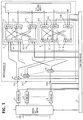
- FIG. 1 An ATM (asynchronous transfer mode) switching system of the present invention for an optical communications network is shown in Fig. 1.
- the switching system includes a bi-directional photonic cross-connect switch 1 whose terminals are used either as incoming ports or outgoing ports and to these ports are connected a plurality of optical fiber transmission links 2 and a plurality of replaceable interface units 3-1 through 3-K.
- These interface units are provided for interfacing between the optical ports of switch 1 and electrical ports 14-1 through 14-k of an ATM switch module 13, and are implemented either with an electro-optical converter, an opto-electrical converter or both for operating as an incoming, outgoing or two-way interface. Details of the interface circuits will be discussed later with reference to Figs. 2A to 2D.
- Switch module 13 is an integrated-circuit module in which are integrated a plurality of directional switches 4-1 through 4-K, an input distribution network 5, an N x M self-routing switch 8 and an output distribution network 9.
- Each of the directional switches 4 has an upper and a lower terminal and sets up a connection between a corresponding electrical port 14 of the module 13 and either of its upper and lower terminals depending on the direction of signals passing through it.
- the input distribution network 5 comprises a plurality of selectors 6-1 through 6-K corresponding in number to switches 4 and a plurality of multiplexers 7-1 through 7-N corresponding in number to the input ports I1 through IN of the self-routing switch 8.
- Each selector 6 has one input port connected to the upper terminal of the corresponding switch 4 and N output ports and each multiplexer 7 has K input ports and one output port connected to the corresponding input port of self-routing switch 8.
- the output distribution network 9 comprises a plurality of demultiplexers 10-1 through 10-M corresponding in number to the output ports O1 through OM of the self-routing switch 8 and a plurality of multiplexer 11-1 through 11-K corresponding in number to switches 4.
- Each demultiplexer 10 has one input port connected to the corresponding output port of self-routing switch 8 and K output ports and each multiplexer 11 has M input ports and one output port connected to the lower terminal of the corresponding switch 4.
- An OAM (operations, administration and maintenance) controller 12 is provided for receiving control data from each interface unit 3 regarding the operating mode of the interface and its maximum operating speed and uses the control data to control the photonic switch 1, directional switches 4, selectors 6 and demultiplexers 10.
- Interface units 3 of different operating modes are shown in Figs. 2A to 2D.
- a mixed combination of interface units 3 are installed to meet the traffic requirements of a particular network node.
- the interface unit of the operating mode shown at 3A in Fig. 2A is an outgoing interface and is implemented with an electro-optical converter 20 and a register 21 in which data concerning the operating mode of the interface unit 3A and its maximum operating speed are stored.
- the E/O converter 20 is connected through terminal 22 to a corresponding electrical output port 14-A and through terminal 23 to the photonic switch 1.
- the data stored in register 21 are supplied via terminal 24 to the controller 12.
- the interface unit of the operating mode shown at 3B in Fig. 2B is an incoming interface and is implemented with an opto-electrical converter 25 and a register 26 in which data concerning the operating mode of the interface unit 3B and its maximum operating speed are stored.
- the O/E converter 25 is connected through terminal 27 to the photonic switch 1 and through terminal 28 to the corresponding electrical input port 14-B, and the data stored in register 26 are supplied via terminal 29 to the controller 12.
- the interface unit of the operating mode shown at 3C in Fig. 2C is an incoming/outgoing interface and is implemented with an electro-optical converter 30, an opto-electrical converter 31 and a register 32.
- the converters 30 and 31 are connected by a manual switch 33 to a terminal 35 and by a manual switch 34 to a terminal 36.
- manual switches 33 and 34 are moved to upper position, and terminal 35 and an electrical output port 14-C1 are connected by a conductor 38 and terminal 36 and the switch 1 is connected by a conductor 39.
- the interface unit of the operating mode shown at 3D in Fig. 2D is a two-way (full-duplex mode) interface and is implemented with an E/O converter 45, an O/E converter 46 and a register 47 in which data indicating this operating mode of interface and its maximum operating speed are stored.
- the E/O converter 45 is connected through terminal 48 to an electrical output port 14-D1 and through terminal 49 to the switch 1 and the O/E converter 46 is connected through terminal 50 to the switch 1 and through terminal 51 to an electrical input port 14-D1.
- the data stored in register 47 are supplied via terminal 52 to the controller 12.
- Controller 12 includes a memory, not shown, in which the bandwidth (operating speed) data of each port of the self-routing switch 8 are stored. Using the data supplied from the interface units 3, the controller 12 makes a search through the memory for corresponding bandwidths and determines the mux/demux distribution of the networks 5 and 6.
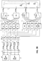
- O/E converters 3-1 and 3-3 are installed for reception of incoming signals from the nodes 60, 61 and 50-Mbps
- 100-Mbps and 200-Mbps E/O converters 3-2, 3-4 and 3-5 are installed for transmission of outgoing signals to the nodes 60, 61.
- the controller 12 receives the operating mode and operating speed data from all the interface units 3 and operates the directional switches 4-1 and 4-3 so that they respectively connect the O/E converters 3-1 and 3-3 to selectors 6-1 and 6-3 and operates the directional switches 3-2, 3-4 and 3-5 so that they respectively connect multiplexers 11-2, 11-4 and 11-5 to the E/O converters 3-2, 3-4 and 3-5.
- controller 12 controls the selectors 6-1 and 6-3 to establish respective connections to multiplexers 9-1 and 9-2 so that the provider's 300-Mbps data is transmitted through multiplexer 9-1 to the input port I1 of self-routing switch 8 and the 50-Mbps data of node 61 is transmitted through multiplexer 9-2 to the input port I2.
- the controller 12 further controls the demultiplexers 10-1 and 10-2 to establish connections from the output port O1 to multiplexers 11-2 and 11-5 and a connection from the output port O2 to multiplexer 11-5.
- each of the demultiplexers 10-1 and 10-2 examines the header of ATM cells from the self-routing switch 8 to identify the data source and disassembles the cells according to the identified data sources into data streams and directs the data streams to appropriate one of multiplexers 11 according to the control signal from the controller 12.
- demultiplexer 10-1 disassembles the data stream from the output port O1 into 50-Mbps and 100-Mbps data streams using the contents of their headers and directs these data streams to multiplexers 11-2 and 11-4 which are specified by the controller 12.
- the provider's 100-Mbps and 200-Mbps data are separated from each other and respectively self-routed to output ports O1 and O2.
- the 100-Mbps data is transmitted from output port O1 through demultiplexer 10-1 and multiplexer 11-4 to the E/O converter 3-4, while the 200-Mbps data is transmitted from output port O2 through demultiplexer 10-2 and multiplexer 11-5 to the E/O converter 3-5.
- the 50-Mbps data of node 61 is self-routed to the output port O1, for example, and transmitted via demultiplexer 10-1 and multiplexer 11-2 to the E/O converter 3-2.
- the arrangement of the interface units 3 is correspondingly modified and the controller 12 responds to this modification by controlling the directional switches 4 and reconfiguring the input and output distribution networks 5 and 9 while meeting the requirements that the total speed of incoming signals to the interface units 3 is equal to the total speed of the input ports of the self-routing switch 8 and the total speed of outgoing signals from the interface units 3 is equal to the total speed of the output ports of the switch 8.
- the controller 12 is notified of this change and reconfigures the networks 5 and 9 by controlling the multiplexer 9-1 to multiplex the outgoing data streams of these nodes and controlling the demultiplexer 10-1 to separate its 200-Mbps input data stream from the self-routing switch 8 into two 100-Mbps data streams and supplies them to multiplexers 11-2 and 11-4 respectively for transmission to nodes 60 and 61.
- the self-routing switch 8 can be operated with a high utilization efficiency.
- the bi-directional photonic cross-connect switch 1 is implemented with a matrix array of bi-directional photonic switching elements 74 respectively connected to the cross-points of row optical waveguides 71 and column optical waveguides 72.
- the optical fiber transmission links 2 are connected via ports 70 to the row waveguides 71 and the column waveguides 72 are connected via ports 73 to the interface units 3.
- Each of the switching elements 74 has a control terminal 75 connected to a corresponding output terminal of a switch controller 76 where control data from the controller 12 are converted to an appropriate voltage signal.
- each photonic switching element 74 applies a control voltage to the control terminal 75 of each photonic switching element 74 to establish a connection at the cross-point of the corresponding row and column waveguides.
- Each photonic switching element 74 is formed of a dielectric substance whose diffraction coefficient is varied in accordance with the level of the control voltage to vary its light transmissivity. Since the photonic cross-connect switch 1 is bi-directional, the connection between the optical links 2 and the interface units 3 can be flexibly reconfigured. Furthermore, the photonic switch 1 can be advantageously implemented on a chip size with dimensions of 110 (mm) x 12 (mm) x 6 (mm) for an 8 x 8 switching distribution.
- each interface unit 3 is implemented with an O/E converter 80, an E/O converter 81, a manually operated optical switch 82 and a register 83 in which data indicating the operating mode (incoming or outgoing mode) of the interface and its operating speed are stored.
- a corresponding port of the photonic switch 1 is connected to a terminal 84.
- Switch 82 is used to connect the corresponding port of the switch via terminal 84 to the input of O/E converter 80 when the interface operates in the incoming mode or connect the output of E/O converter 81 to the terminal 84 when the interface operates in the outgoing mode.
- the output of O/E converter 80 is connected via an output terminal 85 and a corresponding input terminal of the switch module 13 to the selector 6-1.
- the output terminal of multiplexer 11-1 is connected via a corresponding output terminal 88 and an input terminal 86 of interface 3-1 to the input of E/O converter 81.
- the data stored in registers 83 of all interface units 3 are collected by the controller 12 where they are used to control the selectors 6-1 through 6-K and demultiplexers 10-1 through 10M.
Landscapes
- Engineering & Computer Science (AREA)
- Computer Networks & Wireless Communication (AREA)
- Signal Processing (AREA)
- Physics & Mathematics (AREA)
- Mathematical Physics (AREA)
- Data Exchanges In Wide-Area Networks (AREA)
- Use Of Switch Circuits For Exchanges And Methods Of Control Of Multiplex Exchanges (AREA)
- Small-Scale Networks (AREA)
- Optical Communication System (AREA)
Applications Claiming Priority (3)
| Application Number | Priority Date | Filing Date | Title |
|---|---|---|---|
| JP25181/96 | 1996-02-13 | ||
| JP2518196 | 1996-02-13 | ||
| JP2518196A JP2795249B2 (ja) | 1996-02-13 | 1996-02-13 | 非同期転送モードスイッチモジュールおよびネットワーク装置 |
Publications (3)
| Publication Number | Publication Date |
|---|---|
| EP0790724A2 true EP0790724A2 (de) | 1997-08-20 |
| EP0790724A3 EP0790724A3 (de) | 2000-02-23 |
| EP0790724B1 EP0790724B1 (de) | 2003-05-21 |
Family
ID=12158835
Family Applications (1)
| Application Number | Title | Priority Date | Filing Date |
|---|---|---|---|
| EP97102259A Expired - Lifetime EP0790724B1 (de) | 1996-02-13 | 1997-02-12 | ATM-Schaltsystem mit Verteilernetzwerken für variable Verkehrsmuster |
Country Status (5)
| Country | Link |
|---|---|
| US (1) | US5907551A (de) |
| EP (1) | EP0790724B1 (de) |
| JP (1) | JP2795249B2 (de) |
| CA (1) | CA2197382C (de) |
| DE (1) | DE69722051T2 (de) |
Cited By (1)
| Publication number | Priority date | Publication date | Assignee | Title |
|---|---|---|---|---|
| EP1298956A1 (de) * | 2001-10-01 | 2003-04-02 | Alcatel | Direktionales Rekonfigurierbares Optisches System |
Families Citing this family (10)
| Publication number | Priority date | Publication date | Assignee | Title |
|---|---|---|---|---|
| US6643042B1 (en) * | 1997-07-30 | 2003-11-04 | Nec Corporation | Optical communication network node |
| JP2000201163A (ja) * | 1999-01-06 | 2000-07-18 | Nec Corp | 分散型ネットワ―クノ―ド |
| JP3539551B2 (ja) * | 1999-11-16 | 2004-07-07 | 日本電気株式会社 | 共通搬送波上への異種データトラヒック収容フレーム及び伝送装置 |
| US6377725B1 (en) * | 2000-04-10 | 2002-04-23 | Lockheed Martin Corporation | Optical wavelength division multiplexed interconnect system providing autonomous information selection and prioritization |
| JP4588259B2 (ja) * | 2000-09-11 | 2010-11-24 | 富士通株式会社 | 通信システム |
| FR2845224B1 (fr) * | 2002-09-26 | 2004-12-17 | Cit Alcatel | Dispositif ordonnanceur pour un systeme a ressources partagees asymetriquement |
| JP4279583B2 (ja) * | 2003-03-28 | 2009-06-17 | シーケーディ株式会社 | アクチュエータ |
| US20050030889A1 (en) * | 2003-08-04 | 2005-02-10 | Lucent Technologies Inc. | Method and system for transmiting in-band call processing-related traffic using bearer facilities |
| US20060093130A1 (en) * | 2004-10-28 | 2006-05-04 | Utstarcom, Inc. | Automated access network cross-connect system |
| CN102832516B (zh) * | 2012-08-14 | 2014-12-17 | 四川汇源光通信有限公司 | 集成光纤网络接口的墙面电源插线面板 |
Citations (3)
| Publication number | Priority date | Publication date | Assignee | Title |
|---|---|---|---|---|
| EP0386772A2 (de) * | 1989-03-09 | 1990-09-12 | Canon Kabushiki Kaisha | Optische Schaltanordnung zur bidirektionalen Signalübertragung zwischen mehreren Endeinrichtungen |
| US5157654A (en) * | 1990-12-18 | 1992-10-20 | Bell Communications Research, Inc. | Technique for resolving output port contention in a high speed packet switch |
| US5436748A (en) * | 1992-04-30 | 1995-07-25 | Societe Anonyme Dite: Alcatel Cit | Automatically configurable optical system for connecting customer premises networks to a switching center of a telecommuncation network |
Family Cites Families (5)
| Publication number | Priority date | Publication date | Assignee | Title |
|---|---|---|---|---|
| US5740156A (en) * | 1986-09-16 | 1998-04-14 | Hitachi, Ltd. | Packet switching system having self-routing switches |
| DE69228364T2 (de) * | 1991-11-29 | 1999-06-17 | Nec Corp | Optisch ATM-Selbstlenkungsvermittlungssystem mit einer verringerten Zellenkopfbitanzahl |
| JPH05244187A (ja) * | 1992-02-14 | 1993-09-21 | Nippon Telegr & Teleph Corp <Ntt> | 装置内監視方法 |
| JP3291122B2 (ja) * | 1994-06-02 | 2002-06-10 | 富士通株式会社 | 自己ルーチング交換機、atm交換機及び交換システム |
| JP3516490B2 (ja) * | 1994-10-04 | 2004-04-05 | 富士通株式会社 | 回線インタフェース装置 |
-
1996
- 1996-02-13 JP JP2518196A patent/JP2795249B2/ja not_active Expired - Fee Related
-
1997
- 1997-02-12 EP EP97102259A patent/EP0790724B1/de not_active Expired - Lifetime
- 1997-02-12 DE DE69722051T patent/DE69722051T2/de not_active Expired - Fee Related
- 1997-02-12 CA CA002197382A patent/CA2197382C/en not_active Expired - Fee Related
- 1997-02-13 US US08/800,186 patent/US5907551A/en not_active Expired - Lifetime
Patent Citations (3)
| Publication number | Priority date | Publication date | Assignee | Title |
|---|---|---|---|---|
| EP0386772A2 (de) * | 1989-03-09 | 1990-09-12 | Canon Kabushiki Kaisha | Optische Schaltanordnung zur bidirektionalen Signalübertragung zwischen mehreren Endeinrichtungen |
| US5157654A (en) * | 1990-12-18 | 1992-10-20 | Bell Communications Research, Inc. | Technique for resolving output port contention in a high speed packet switch |
| US5436748A (en) * | 1992-04-30 | 1995-07-25 | Societe Anonyme Dite: Alcatel Cit | Automatically configurable optical system for connecting customer premises networks to a switching center of a telecommuncation network |
Non-Patent Citations (2)
| Title |
|---|
| AHMADI H ET AL: "A HIGH-PERFORMANCE SWITCH FABRIC FOR INTEGRATED CIRCUIT AND PACKET SWITCHING" PROCEEDINGS OF THE ANNUAL JOINT CONFERENCE OF THE COMPUTER AND COMMUNICATIONS SOCIETIES. (INFOCOM),US,NEW YORK, IEEE, vol. CONF. 7, page 9-18 XP000010853 ISBN: 0-8186-0833-1 * |
| FRANKLIN M A ET AL: "INTERCONNECTION NETWORKS: PHYSICAL DESIGN AND PERFORMANCE ANALYSIS" JOURNAL OF PARALLEL AND DISTRIBUTED COMPUTING,US,ACADEMIC PRESS, DULUTH, MN, vol. 3, no. 3, page 352-372 XP000084803 ISSN: 0743-7315 * |
Cited By (3)
| Publication number | Priority date | Publication date | Assignee | Title |
|---|---|---|---|---|
| EP1298956A1 (de) * | 2001-10-01 | 2003-04-02 | Alcatel | Direktionales Rekonfigurierbares Optisches System |
| FR2830333A1 (fr) * | 2001-10-01 | 2003-04-04 | Cit Alcatel | Systeme optique directionnel re-configurable |
| US7254328B2 (en) | 2001-10-01 | 2007-08-07 | Alcatel | Reconfigurable directional optical system |
Also Published As
| Publication number | Publication date |
|---|---|
| CA2197382A1 (en) | 1997-08-14 |
| EP0790724B1 (de) | 2003-05-21 |
| JP2795249B2 (ja) | 1998-09-10 |
| CA2197382C (en) | 2002-01-08 |
| DE69722051T2 (de) | 2003-11-27 |
| JPH09219707A (ja) | 1997-08-19 |
| US5907551A (en) | 1999-05-25 |
| EP0790724A3 (de) | 2000-02-23 |
| DE69722051D1 (de) | 2003-06-26 |
Similar Documents
| Publication | Publication Date | Title |
|---|---|---|
| US7274702B2 (en) | Programmable interconnect system for scalable router | |
| EP0720322B1 (de) | Optisches Kommunikations-Zugangs-Netzwerk mit einem Multiplexer/Demultiplexer in jeder Netzabschlusseinrichtung | |
| KR100194813B1 (ko) | 멀티채널/멀티캐스트 스위칭 기능을 갖는 패킷 스위칭장치 및 이를 이용한 패킷 스위칭 시스템 | |
| US7526203B2 (en) | Apparatus and method for optical switching at an optical switch fabric | |
| CA2285128C (en) | Switch for optical signals | |
| US6738540B2 (en) | Optical cross-connect switch using programmable multiplexers/demultiplexers | |
| EP0741499A2 (de) | Blockierungsfreie optische Querverbindungsstruktur für ein Fernmeldenetz | |
| US20040037290A1 (en) | Switching device for telecommunication networks | |
| JPH0773394B2 (ja) | 異種通信網の一元的通信網への統合方法 | |
| KR19980064825A (ko) | 에이.티.엠 스위치의 분산 버퍼링 시스템 | |
| US20120243868A1 (en) | High capacity switching system | |
| US5907551A (en) | ATM switching system with distribution networks for varying traffic patterns | |
| KR960706730A (ko) | 협소대역 통신용 ATM 망(ATM networks for narrowband communications) | |
| JPH09507996A (ja) | 大容量モジュールatmスイッチ | |
| US6185021B1 (en) | Cross-connecting optical translator array | |
| US20030152072A1 (en) | Routing device for all optical networks | |
| US20040258411A1 (en) | Node for an optical network | |
| US6104723A (en) | Network for packet-oriented data traffic | |
| US6643042B1 (en) | Optical communication network node | |
| US6940860B2 (en) | Network node for ATM transmission system | |
| KR100284004B1 (ko) | 수요밀집형 광가입자 전송장치에 있어서의 호스트 디지털 터미널 | |
| JP2000092000A (ja) | 完全な網目状光コア伝送ネットワ―クを有する大規模通信ネットワ―ク | |
| JP2581249B2 (ja) | クロスコネクト網構成方法 | |
| Buhrgard | Photonic Switching of Optical Interconnects in Large Telecom Nodes | |
| WO2001074111A1 (en) | Routing device for all optical networks |
Legal Events
| Date | Code | Title | Description |
|---|---|---|---|
| PUAI | Public reference made under article 153(3) epc to a published international application that has entered the european phase |
Free format text: ORIGINAL CODE: 0009012 |
|
| AK | Designated contracting states |
Kind code of ref document: A2 Designated state(s): DE FR GB IT NL SE |
|
| PUAL | Search report despatched |
Free format text: ORIGINAL CODE: 0009013 |
|
| AK | Designated contracting states |
Kind code of ref document: A3 Designated state(s): DE FR GB IT NL SE |
|
| 17P | Request for examination filed |
Effective date: 20000121 |
|
| 17Q | First examination report despatched |
Effective date: 20011210 |
|
| GRAH | Despatch of communication of intention to grant a patent |
Free format text: ORIGINAL CODE: EPIDOS IGRA |
|
| GRAH | Despatch of communication of intention to grant a patent |
Free format text: ORIGINAL CODE: EPIDOS IGRA |
|
| GRAA | (expected) grant |
Free format text: ORIGINAL CODE: 0009210 |
|
| AK | Designated contracting states |
Designated state(s): DE FR GB IT NL SE |
|
| PG25 | Lapsed in a contracting state [announced via postgrant information from national office to epo] |
Ref country code: NL Free format text: LAPSE BECAUSE OF FAILURE TO SUBMIT A TRANSLATION OF THE DESCRIPTION OR TO PAY THE FEE WITHIN THE PRESCRIBED TIME-LIMIT Effective date: 20030521 Ref country code: IT Free format text: LAPSE BECAUSE OF FAILURE TO SUBMIT A TRANSLATION OF THE DESCRIPTION OR TO PAY THE FEE WITHIN THE PRE;WARNING: LAPSES OF ITALIAN PATENTS WITH EFFECTIVE DATE BEFORE 2007 MAY HAVE OCCURRED AT ANY TIME BEFORE 2007. THE CORRECT EFFECTIVE DATE MAY BE DIFFERENT FROM THE ONE RECORDED.SCRIBED TIME-LIMIT Effective date: 20030521 |
|
| REG | Reference to a national code |
Ref country code: GB Ref legal event code: FG4D |
|
| REF | Corresponds to: |
Ref document number: 69722051 Country of ref document: DE Date of ref document: 20030626 Kind code of ref document: P |
|
| PG25 | Lapsed in a contracting state [announced via postgrant information from national office to epo] |
Ref country code: SE Free format text: LAPSE BECAUSE OF FAILURE TO SUBMIT A TRANSLATION OF THE DESCRIPTION OR TO PAY THE FEE WITHIN THE PRESCRIBED TIME-LIMIT Effective date: 20030821 |
|
| NLV1 | Nl: lapsed or annulled due to failure to fulfill the requirements of art. 29p and 29m of the patents act | ||
| PG25 | Lapsed in a contracting state [announced via postgrant information from national office to epo] |
Ref country code: GB Free format text: LAPSE BECAUSE OF NON-PAYMENT OF DUE FEES Effective date: 20040212 |
|
| ET | Fr: translation filed | ||
| PLBE | No opposition filed within time limit |
Free format text: ORIGINAL CODE: 0009261 |
|
| STAA | Information on the status of an ep patent application or granted ep patent |
Free format text: STATUS: NO OPPOSITION FILED WITHIN TIME LIMIT |
|
| 26N | No opposition filed |
Effective date: 20040224 |
|
| GBPC | Gb: european patent ceased through non-payment of renewal fee |
Effective date: 20040212 |
|
| REG | Reference to a national code |
Ref country code: FR Ref legal event code: TP |
|
| PGFP | Annual fee paid to national office [announced via postgrant information from national office to epo] |
Ref country code: DE Payment date: 20090206 Year of fee payment: 13 |
|
| PGFP | Annual fee paid to national office [announced via postgrant information from national office to epo] |
Ref country code: FR Payment date: 20090213 Year of fee payment: 13 |
|
| REG | Reference to a national code |
Ref country code: FR Ref legal event code: ST Effective date: 20101029 |
|
| PG25 | Lapsed in a contracting state [announced via postgrant information from national office to epo] |
Ref country code: FR Free format text: LAPSE BECAUSE OF NON-PAYMENT OF DUE FEES Effective date: 20100301 |
|
| PG25 | Lapsed in a contracting state [announced via postgrant information from national office to epo] |
Ref country code: DE Free format text: LAPSE BECAUSE OF NON-PAYMENT OF DUE FEES Effective date: 20100901 |