EP0785589A1 - Circuit selection device - Google Patents
Circuit selection device Download PDFInfo
- Publication number
- EP0785589A1 EP0785589A1 EP97100636A EP97100636A EP0785589A1 EP 0785589 A1 EP0785589 A1 EP 0785589A1 EP 97100636 A EP97100636 A EP 97100636A EP 97100636 A EP97100636 A EP 97100636A EP 0785589 A1 EP0785589 A1 EP 0785589A1
- Authority
- EP
- European Patent Office
- Prior art keywords
- terminal
- output
- input
- load
- transmission lines
- Prior art date
- Legal status (The legal status is an assumption and is not a legal conclusion. Google has not performed a legal analysis and makes no representation as to the accuracy of the status listed.)
- Withdrawn
Links
- 230000005540 biological transmission Effects 0.000 claims abstract description 46
- 238000010586 diagram Methods 0.000 description 7
- 230000037431 insertion Effects 0.000 description 7
- 238000003780 insertion Methods 0.000 description 7
- 239000000470 constituent Substances 0.000 description 1
- 230000003247 decreasing effect Effects 0.000 description 1
Images


Classifications
-
- H—ELECTRICITY
- H01—ELECTRIC ELEMENTS
- H01P—WAVEGUIDES; RESONATORS, LINES, OR OTHER DEVICES OF THE WAVEGUIDE TYPE
- H01P1/00—Auxiliary devices
- H01P1/10—Auxiliary devices for switching or interrupting
Definitions
- the present invention relates to an RF circuit and, more particularly, to a device for selecting one of a plurality of RF signal circuits in a mobile radio telephone set.
- phase shifter based on a line length switching scheme of switching two transmission lines having different line lengths by using a switch
- This phase shifter includes first and second transmission lines which have a predetermined line length difference and each of which has one end connected to an input terminal and the other end connected to an output terminal, and a switch which switches between the OFF state and the ON state. In the ON state, the switch is connected to predetermined positions on the first and second transmission lines such that an open-circuit impedance value appears when viewed from the input and output terminals.
- the phase shifter having such an arrangement switches the transmission lines through which radio waves pass by switching the switch between the ON state and the OFF state, thereby changing the phases of the radio waves.
- the switch to be used may be constituted by a plurality of two-way switched or one multi-way switch.
- phase shifter for changing a phase.
- This phase shifter has constituent elements similar to those of a circuit selection device, but has no circuit selecting function.
- a circuit selection device When a circuit selection device is constituted by a plurality of two-way switches, an input signal must pass through the switches until it reaches the output terminal. With an increase in the number of circuits which can he selected, an input signal passes through a larger number of switches. As a result, the overall insertion loss of the switching device increases.
- circuit selection device is constituted by a multi-way switch.
- a general multi-way switch currently on the market tends to have a large insertion loss, and is expensive. If the insertion loss of the switch of the circuit selection device can be minimized, the gains of other circuits need not be increased. For this reason, the device is required to suppress the insertion loss.
- a circuit selection device comprising a first terminal to/from which an RF signal is input/output, a plurality of transmission lines each having one end connected to the first terminal, a plurality of second terminals each arranged in correspondence with the other end of each of the transmission lines to selectively input/output an RF signal input/output to/from the first terminal, a plurality of loads for impedance matching, each of the loads being arranged in correspondence with the other end of each of the transmission lines, and a plurality of switches each switched/connected to one of the second terminal and the load which correspond to the other end of each of the transmission lines, wherein when one of the switches is switched to a second terminal side, the remaining switches are switched to a load side.
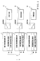
- Fig. 1 shows a circuit selection device according to the first embodiment of the present invention and explains the principle of the circuit selection device.
- an input terminal 1 is connected to one end of each of a first transmission line 3, a second transmission line 4, and a switch 6 through a node 2.
- the other end of the first transmission line 3 is connected to the input terminal of a switch 6.
- the first output terminal of the switch 6 is connected to a first output terminal 12.
- the output terminal of the switch 6 is connected to a first load 9.
- the other end of the second transmission line 4 is connected to the input side of a switch 7.
- the first output side of the switch 7 is connected to a second output terminal 13.
- the second output side of the switch 7 is connected to a second load 10.
- the other end of the third transmission line 5 is connected to the input side of a switch 8.
- the first output side of the switch 8 is connected to a third output terminal 14.
- the second output side of the switch 8 is connected to a third load 11.
- the first, second, and third transmission lines 3 to 5 have the same line length.
- the first, second, and third loads 9 to 11 have the same impedance.
- Reference numerals 3a, 4a, and 5a denote disconnecting circuits for disconnecting the first, second, and third loads 9 to 11 in accordance with line lengths; and 3b, 4b, and 5b, short-circuiting circuits for open-/short-circuiting the first, second, and third loads in accordance with line lengths.
- the line length of the second transmission line 4 and the impedance of the second load 10 are determined such that an open-circuit impedance is set at the signal frequency between the second transmission line 4 and the second load 10 when viewed from the node 2.
- the line length of the second transmission line 4 corresponds to 1/2 the wavelength, it suffices if the second load 10 is disconnected by the disconnecting circuit 4a.
- the line length of the second transmission line 4 corresponds to the 1/4 the wavelength, it suffices if the second load 10 is short-circuited by the short-circuiting circuit 4b.
- an open-circuit impedance is set at the signal frequency between the third transmission line 5 and the load 11, when viewed from the node 2, by the disconnecting circuit 5a or 5b.
- the line length of the second transmission line 4 is to be decreased in consideration of a mounting area or the like, it suffices if the line length of the second transmission line 4 is determined to set an open-circuit impedance, when viewed from the node 2, by using the inductance of the second load 10.
- Fig. 2 shows this state.
- the second transmission line 4 and the third transmission line 5 are connected to the node 2.
- each impedance is an open-circuit impedance when viewed from the node 2
- Fig. 2 does not show the second and third transmission lines 4 and 5.
- an RF signal is output from the input terminal 1 to the first output terminal 12 through the first transmission line 3 and the switch 6. If the impedances connected to the input terminal 1 and the first to third output terminals 12 to 14 are equal, no impedance mismatch occurs.
- the switches connected to the remaining output terminals are switched to the load side. For this reason, since the combined impedance at the transmission lines, the switches, and the signal frequency at the loads is an open-circuit impedance, even if the number of output terminals which can be selected increases, a signal is output to the selected output terminal without causing any mismatch. In addition, since the signal passes through one switch between the input and output terminals, the insertion loss can be minimized.
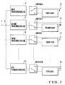
- Fig. 3 shows the second embodiment of the present invention.
- the first embodiment includes three output terminals
- the second embodiment includes four or more output terminals.
- Reference numeral 15 denotes an nth transmission line; 16, an nth switch; 17, an nth load, and 18, an nth output terminal.
- a first switch 6 connected to a first output terminal 12 to which a signal is to be output is switched to the first output terminal 12 side, while all remaining switches 13, 14,..., and the switch 16 are switched to loads 10, 11,..., and the load 17.
- Fig. 2 shows an equivalent circuit diagram in this state.
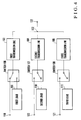
- Fig. 4 shows an arrangement including a plurality of input terminals and one output terminal according to the third embodiment of the present invention.
- the position of the input terminal and the positions of the output terminals in Fig. 1 are reversed.
- the first and second input sides of a first switch 106 are respectively connected to a first input terminal 119 and a first load 109.
- the output side of the first switch 106 is connected to one end of a first transmission line 103.
- the first and second input sides of a second switch 107 are respectively connected to a second input terminal 120 and a second load 110.
- the output side of the second switch 107 is connected to one end of a second transmission line 104.
- the first and second input sides of a third switch 108 are respectively connected to a third input terminal 121 and a third load 111.
- the output side of the third switch 108 is connected to one end of a third transmission line 105.
- the other end of each of the first to third transmission lines 103, 104, and 105 is commonly connected to an output terminal 122 through a node 102.
- Fig. 5 is an equivalent circuit diagram in this state.
- circuit selection device of the present invention when one of a plurality of output terminals (input terminals) is selected, and a signal is to be output (input) thereto, it suffices if a signal passes through one of two-way switches. Therefore, the insertion loss between the input and output terminals can be minimized.
- the circuit selection device of the present invention even if the number of output terminals (input terminals) increases, when a switch is switched to the load side, the impedance viewed from the node between the transmission line and the load is an open-circuit impedance. For this reason, the characteristics between the input and output terminals are not influenced.
Landscapes
- Waveguide Switches, Polarizers, And Phase Shifters (AREA)
- Transmitters (AREA)
- Cable Transmission Systems, Equalization Of Radio And Reduction Of Echo (AREA)
Applications Claiming Priority (2)
| Application Number | Priority Date | Filing Date | Title |
|---|---|---|---|
| JP8006538A JPH09199902A (ja) | 1996-01-18 | 1996-01-18 | 回路選択装置 |
| JP6538/96 | 1996-01-18 |
Publications (1)
| Publication Number | Publication Date |
|---|---|
| EP0785589A1 true EP0785589A1 (en) | 1997-07-23 |
Family
ID=11641133
Family Applications (1)
| Application Number | Title | Priority Date | Filing Date |
|---|---|---|---|
| EP97100636A Withdrawn EP0785589A1 (en) | 1996-01-18 | 1997-01-16 | Circuit selection device |
Country Status (4)
| Country | Link |
|---|---|
| US (1) | US5783975A (ja) |
| EP (1) | EP0785589A1 (ja) |
| JP (1) | JPH09199902A (ja) |
| AU (1) | AU708483B2 (ja) |
Cited By (1)
| Publication number | Priority date | Publication date | Assignee | Title |
|---|---|---|---|---|
| CN103296997A (zh) * | 2012-02-21 | 2013-09-11 | 德克萨斯仪器股份有限公司 | 传输线脉冲发送 |
Families Citing this family (6)
| Publication number | Priority date | Publication date | Assignee | Title |
|---|---|---|---|---|
| US6097266A (en) * | 1998-08-14 | 2000-08-01 | Lucent Technologies Inc | Intelligent RF combiner |
| FR2803147B1 (fr) * | 1999-12-23 | 2002-12-06 | Cit Alcatel | Organe de communication electronique a une entree et plusieurs sorties et son application a une matrice de commutation |
| GB2359666B (en) * | 2000-02-24 | 2004-06-23 | Wireless Systems Int Ltd | A signal combiner, a signal splitter and a circuit using a combiner and a splitter |
| US20030216488A1 (en) * | 2002-04-18 | 2003-11-20 | The Procter & Gamble Company | Compositions comprising a dispersant and microcapsules containing an active material |
| US8049574B2 (en) * | 2009-05-18 | 2011-11-01 | Lockheed Martin Corporation | High power UHF single-pole multi-throw switch |
| CN115004571B (zh) * | 2019-12-17 | 2024-12-17 | 门罗微系统公司 | 差分时间延迟移位器、对信号施加时间延迟的方法和系统 |
Citations (4)
| Publication number | Priority date | Publication date | Assignee | Title |
|---|---|---|---|---|
| US4556808A (en) * | 1982-06-03 | 1985-12-03 | Texas Instruments Incorporated | Microwave monolithic spot FET switch configuration |
| WO1987000696A1 (en) * | 1985-07-18 | 1987-01-29 | Hughes Aircraft Company | Active microwave switcher |
| JPH0432301A (ja) | 1990-05-29 | 1992-02-04 | Mitsubishi Electric Corp | 移相器 |
| JPH0722802A (ja) * | 1993-06-29 | 1995-01-24 | New Japan Radio Co Ltd | 伝送線路スイッチ |
Family Cites Families (5)
| Publication number | Priority date | Publication date | Assignee | Title |
|---|---|---|---|---|
| GB801062A (en) * | 1955-10-19 | 1958-09-10 | Rank Cintel Ltd | Improvements in or relating to signal selection circuits |
| US2958054A (en) * | 1958-11-24 | 1960-10-25 | Amphenol Borg Electronics Corp | Impedance terminated coaxial line switch apparatus |
| US3694775A (en) * | 1971-03-29 | 1972-09-26 | Gen Dynamics Corp | Matrix switching system having iteratively terminated transmission line |
| US3808566A (en) * | 1973-05-24 | 1974-04-30 | Gen Dynamics Corp | Switching system |
| US5274343A (en) * | 1991-08-06 | 1993-12-28 | Raytheon Company | Plural switch circuits having RF propagation networks and RF terminations |
-
1996
- 1996-01-18 JP JP8006538A patent/JPH09199902A/ja active Pending
-
1997
- 1997-01-16 US US08/783,870 patent/US5783975A/en not_active Expired - Fee Related
- 1997-01-16 EP EP97100636A patent/EP0785589A1/en not_active Withdrawn
- 1997-01-17 AU AU12215/97A patent/AU708483B2/en not_active Ceased
Patent Citations (4)
| Publication number | Priority date | Publication date | Assignee | Title |
|---|---|---|---|---|
| US4556808A (en) * | 1982-06-03 | 1985-12-03 | Texas Instruments Incorporated | Microwave monolithic spot FET switch configuration |
| WO1987000696A1 (en) * | 1985-07-18 | 1987-01-29 | Hughes Aircraft Company | Active microwave switcher |
| JPH0432301A (ja) | 1990-05-29 | 1992-02-04 | Mitsubishi Electric Corp | 移相器 |
| JPH0722802A (ja) * | 1993-06-29 | 1995-01-24 | New Japan Radio Co Ltd | 伝送線路スイッチ |
Non-Patent Citations (2)
| Title |
|---|
| PATENT ABSTRACTS OF JAPAN vol. 95, no. 4 31 May 1995 (1995-05-31) * |
| Y. TAJIMA ET AL.: "Broadband GaAs FET 2x1 switches", IEEE GALLIUM ARSENIDE INTEGRATED CIRCUIT SYMPOSIUM - TECHNICAL DIGEST, 23 October 1984 (1984-10-23) - 25 October 1984 (1984-10-25), BOSTON (US), pages 81 - 84, XP002030086 * |
Cited By (3)
| Publication number | Priority date | Publication date | Assignee | Title |
|---|---|---|---|---|
| CN103296997A (zh) * | 2012-02-21 | 2013-09-11 | 德克萨斯仪器股份有限公司 | 传输线脉冲发送 |
| US9829526B2 (en) | 2012-02-21 | 2017-11-28 | Texas Instruments Incorporated | Transmission line pulsing |
| CN103296997B (zh) * | 2012-02-21 | 2018-07-13 | 德克萨斯仪器股份有限公司 | 传输线脉冲发送 |
Also Published As
| Publication number | Publication date |
|---|---|
| JPH09199902A (ja) | 1997-07-31 |
| US5783975A (en) | 1998-07-21 |
| AU1221597A (en) | 1997-07-24 |
| AU708483B2 (en) | 1999-08-05 |
Similar Documents
| Publication | Publication Date | Title |
|---|---|---|
| EP0928038B1 (en) | Two-frequency switch, device using two-frequency antenna in common, and mobile radio communication equipment for two-frequency bands using the device | |
| US8248302B2 (en) | Reflection-type phase shifter having reflection loads implemented using transmission lines and phased-array receiver/transmitter utilizing the same | |
| US4733203A (en) | Passive phase shifter having switchable filter paths to provide selectable phase shift | |
| US5519364A (en) | High-frequency switch | |
| US5025225A (en) | Amplifier having substantially constant D.C. to r.f. conversion efficiency | |
| US5778306A (en) | Low loss high frequency transmitting/receiving switching module | |
| US20040132487A1 (en) | Antenna switching circuit | |
| EP1532745B1 (en) | High frequency module | |
| WO2001028029A1 (en) | Rf power divider/combiner circuit | |
| US10763827B1 (en) | Delay line with controllable phase-shifting cells | |
| KR0139477B1 (ko) | 유전체 필터 | |
| JPH10308602A (ja) | 高周波スイッチ回路 | |
| US5486797A (en) | Integrated port selection circuit for high frequency signal | |
| US4165497A (en) | Wideband RF switching matrix | |
| US5148128A (en) | RF digital phase shift modulators | |
| JP3163918B2 (ja) | 高周波スイッチ | |
| US5783975A (en) | Circuit selection device | |
| EP1440511B1 (en) | Compact 180 degree phase shifter | |
| US5369795A (en) | High frequency transformer and mixer using the same | |
| CN117749129A (zh) | 电路 | |
| US6856187B2 (en) | High frequency switch module | |
| CN117749128A (zh) | 电路 | |
| US20020067226A1 (en) | Filter Circuit | |
| US7015770B2 (en) | High frequency switch | |
| US20250309876A1 (en) | Radio-frequency circuit |
Legal Events
| Date | Code | Title | Description |
|---|---|---|---|
| PUAI | Public reference made under article 153(3) epc to a published international application that has entered the european phase |
Free format text: ORIGINAL CODE: 0009012 |
|
| 17P | Request for examination filed |
Effective date: 19970512 |
|
| AK | Designated contracting states |
Kind code of ref document: A1 Designated state(s): DE FR GB IT |
|
| 17Q | First examination report despatched |
Effective date: 20000315 |
|
| STAA | Information on the status of an ep patent application or granted ep patent |
Free format text: STATUS: THE APPLICATION HAS BEEN WITHDRAWN |
|
| 18W | Application withdrawn |
Withdrawal date: 20020409 |