EP0783046B1 - Verfahren und Vorrichtung zum Ziehen eines Einkristalls - Google Patents
Verfahren und Vorrichtung zum Ziehen eines Einkristalls Download PDFInfo
- Publication number
- EP0783046B1 EP0783046B1 EP96119963A EP96119963A EP0783046B1 EP 0783046 B1 EP0783046 B1 EP 0783046B1 EP 96119963 A EP96119963 A EP 96119963A EP 96119963 A EP96119963 A EP 96119963A EP 0783046 B1 EP0783046 B1 EP 0783046B1
- Authority
- EP
- European Patent Office
- Prior art keywords
- shielding part
- monocrystal
- single crystal
- pulling
- beginning
- Prior art date
- Legal status (The legal status is an assumption and is not a legal conclusion. Google has not performed a legal analysis and makes no representation as to the accuracy of the status listed.)
- Expired - Lifetime
Links
- 238000000034 method Methods 0.000 title claims description 12
- 239000013078 crystal Substances 0.000 title description 40
- 239000000155 melt Substances 0.000 claims description 9
- XUIMIQQOPSSXEZ-UHFFFAOYSA-N Silicon Chemical compound [Si] XUIMIQQOPSSXEZ-UHFFFAOYSA-N 0.000 claims description 8
- 229910052710 silicon Inorganic materials 0.000 claims description 8
- 239000010703 silicon Substances 0.000 claims description 8
- OKTJSMMVPCPJKN-UHFFFAOYSA-N Carbon Chemical compound [C] OKTJSMMVPCPJKN-UHFFFAOYSA-N 0.000 claims description 5
- 229910002804 graphite Inorganic materials 0.000 claims description 5
- 239000010439 graphite Substances 0.000 claims description 5
- 239000000463 material Substances 0.000 claims description 4
- 239000010453 quartz Substances 0.000 claims description 2
- VYPSYNLAJGMNEJ-UHFFFAOYSA-N silicon dioxide Inorganic materials O=[Si]=O VYPSYNLAJGMNEJ-UHFFFAOYSA-N 0.000 claims description 2
- 239000000126 substance Substances 0.000 claims description 2
- 239000004065 semiconductor Substances 0.000 description 11
- 235000012431 wafers Nutrition 0.000 description 11
- 238000002425 crystallisation Methods 0.000 description 4
- 230000008025 crystallization Effects 0.000 description 4
- 230000000694 effects Effects 0.000 description 3
- 230000005855 radiation Effects 0.000 description 3
- 238000004519 manufacturing process Methods 0.000 description 2
- 238000011109 contamination Methods 0.000 description 1
- 230000007547 defect Effects 0.000 description 1
- 238000010438 heat treatment Methods 0.000 description 1
- 230000003647 oxidation Effects 0.000 description 1
- 238000007254 oxidation reaction Methods 0.000 description 1
Images

Classifications
-
- C—CHEMISTRY; METALLURGY
- C30—CRYSTAL GROWTH
- C30B—SINGLE-CRYSTAL GROWTH; UNIDIRECTIONAL SOLIDIFICATION OF EUTECTIC MATERIAL OR UNIDIRECTIONAL DEMIXING OF EUTECTOID MATERIAL; REFINING BY ZONE-MELTING OF MATERIAL; PRODUCTION OF A HOMOGENEOUS POLYCRYSTALLINE MATERIAL WITH DEFINED STRUCTURE; SINGLE CRYSTALS OR HOMOGENEOUS POLYCRYSTALLINE MATERIAL WITH DEFINED STRUCTURE; AFTER-TREATMENT OF SINGLE CRYSTALS OR A HOMOGENEOUS POLYCRYSTALLINE MATERIAL WITH DEFINED STRUCTURE; APPARATUS THEREFOR
- C30B15/00—Single-crystal growth by pulling from a melt, e.g. Czochralski method
- C30B15/20—Controlling or regulating
-
- C—CHEMISTRY; METALLURGY
- C30—CRYSTAL GROWTH
- C30B—SINGLE-CRYSTAL GROWTH; UNIDIRECTIONAL SOLIDIFICATION OF EUTECTIC MATERIAL OR UNIDIRECTIONAL DEMIXING OF EUTECTOID MATERIAL; REFINING BY ZONE-MELTING OF MATERIAL; PRODUCTION OF A HOMOGENEOUS POLYCRYSTALLINE MATERIAL WITH DEFINED STRUCTURE; SINGLE CRYSTALS OR HOMOGENEOUS POLYCRYSTALLINE MATERIAL WITH DEFINED STRUCTURE; AFTER-TREATMENT OF SINGLE CRYSTALS OR A HOMOGENEOUS POLYCRYSTALLINE MATERIAL WITH DEFINED STRUCTURE; APPARATUS THEREFOR
- C30B29/00—Single crystals or homogeneous polycrystalline material with defined structure characterised by the material or by their shape
- C30B29/02—Elements
- C30B29/06—Silicon
-
- C—CHEMISTRY; METALLURGY
- C30—CRYSTAL GROWTH
- C30B—SINGLE-CRYSTAL GROWTH; UNIDIRECTIONAL SOLIDIFICATION OF EUTECTIC MATERIAL OR UNIDIRECTIONAL DEMIXING OF EUTECTOID MATERIAL; REFINING BY ZONE-MELTING OF MATERIAL; PRODUCTION OF A HOMOGENEOUS POLYCRYSTALLINE MATERIAL WITH DEFINED STRUCTURE; SINGLE CRYSTALS OR HOMOGENEOUS POLYCRYSTALLINE MATERIAL WITH DEFINED STRUCTURE; AFTER-TREATMENT OF SINGLE CRYSTALS OR A HOMOGENEOUS POLYCRYSTALLINE MATERIAL WITH DEFINED STRUCTURE; APPARATUS THEREFOR
- C30B15/00—Single-crystal growth by pulling from a melt, e.g. Czochralski method
- C30B15/14—Heating of the melt or the crystallised materials
-
- Y—GENERAL TAGGING OF NEW TECHNOLOGICAL DEVELOPMENTS; GENERAL TAGGING OF CROSS-SECTIONAL TECHNOLOGIES SPANNING OVER SEVERAL SECTIONS OF THE IPC; TECHNICAL SUBJECTS COVERED BY FORMER USPC CROSS-REFERENCE ART COLLECTIONS [XRACs] AND DIGESTS
- Y10—TECHNICAL SUBJECTS COVERED BY FORMER USPC
- Y10S—TECHNICAL SUBJECTS COVERED BY FORMER USPC CROSS-REFERENCE ART COLLECTIONS [XRACs] AND DIGESTS
- Y10S117/00—Single-crystal, oriented-crystal, and epitaxy growth processes; non-coating apparatus therefor
- Y10S117/90—Apparatus characterized by composition or treatment thereof, e.g. surface finish, surface coating
-
- Y—GENERAL TAGGING OF NEW TECHNOLOGICAL DEVELOPMENTS; GENERAL TAGGING OF CROSS-SECTIONAL TECHNOLOGIES SPANNING OVER SEVERAL SECTIONS OF THE IPC; TECHNICAL SUBJECTS COVERED BY FORMER USPC CROSS-REFERENCE ART COLLECTIONS [XRACs] AND DIGESTS
- Y10—TECHNICAL SUBJECTS COVERED BY FORMER USPC
- Y10T—TECHNICAL SUBJECTS COVERED BY FORMER US CLASSIFICATION
- Y10T117/00—Single-crystal, oriented-crystal, and epitaxy growth processes; non-coating apparatus therefor
- Y10T117/10—Apparatus
- Y10T117/1024—Apparatus for crystallization from liquid or supercritical state
- Y10T117/1032—Seed pulling
- Y10T117/1068—Seed pulling including heating or cooling details [e.g., shield configuration]
-
- Y—GENERAL TAGGING OF NEW TECHNOLOGICAL DEVELOPMENTS; GENERAL TAGGING OF CROSS-SECTIONAL TECHNOLOGIES SPANNING OVER SEVERAL SECTIONS OF THE IPC; TECHNICAL SUBJECTS COVERED BY FORMER USPC CROSS-REFERENCE ART COLLECTIONS [XRACs] AND DIGESTS
- Y10—TECHNICAL SUBJECTS COVERED BY FORMER USPC
- Y10T—TECHNICAL SUBJECTS COVERED BY FORMER US CLASSIFICATION
- Y10T117/00—Single-crystal, oriented-crystal, and epitaxy growth processes; non-coating apparatus therefor
- Y10T117/10—Apparatus
- Y10T117/1024—Apparatus for crystallization from liquid or supercritical state
- Y10T117/1076—Apparatus for crystallization from liquid or supercritical state having means for producing a moving solid-liquid-solid zone
- Y10T117/1088—Apparatus for crystallization from liquid or supercritical state having means for producing a moving solid-liquid-solid zone including heating or cooling details
Definitions
- the invention relates to a method for pulling a Silicon single crystal from a melt, comprising the Dragging a conical section at the beginning and at the End of the single crystal and pulling a cylindrical one Section between the conical sections.
- the invention also relates to a device for Execution of the procedure.
- the invention represents an improvement in the term "Czochralski method" known method of manufacture of single crystals.
- a Seed crystal that has previously been immersed in a melt is at a certain speed from that Melt surface pulled away, being on its underside a rod-shaped single crystal grows up.
- the diameter of the growing single crystal initially enlarged so that a conical section, the so-called initial cone, arises.
- the diameter of the growing single crystal kept constant and a cylindrical section drawn.
- the resulting section at the end of the single crystal becomes the end cone called. Changes in single crystal diameter go significantly on changes in the drawing speed and on Changes in temperature in the melt, especially in the area of the crystallization limit.
- the diameter of the stacking error ring is proportional to the speed at which the Single crystal was pulled at the time when the semiconductor material that the later extracted Semiconductor wafer, crystallized. At a certain pulling speed disappears Stacking error ring, as it were, because its diameter matches that Diameter of the later semiconductor wafer matches. It therefore tries to pull this pulling speed of the single crystal to quickly reach the occurrence of the Stacking error ring on the initial cone and on one as short as possible part of the adjacent cylindrical Restrict section. However, this is only possible insufficient.
- the Dielectric strength of oxide films which in technical jargon as Gate Oxide Integrity (GOI) is called and an important one Criterion for assessing the quality of Semiconductor wafers represents the pulling speed is indirectly proportional.
- GOI Gate Oxide Integrity
- the object of the present invention was therefore to to improve the process so silicon single crystals can be made with a cylindrical section which almost completely turns into high quality Allows semiconductor wafers to be cut without a stacked fault ring.
- the task is solved by a method of the named Genus, which is characterized in that the surface of the conical section at the beginning of the single crystal a shielding part spaced from the single crystal of 20 to 100% becomes.
- Genus which is characterized in that the surface of the conical section at the beginning of the single crystal a shielding part spaced from the single crystal of 20 to 100% becomes.
- the object is further achieved by a device as claimed in claim 4.
- the shielding part prevents the free heat radiation from the surface of the initial cone into the environment.
- the reduced effects Heat radiation that already at lower Pulling speeds than usual the diameter of the Stacking wreath with the diameter of the growing Single crystal matches.
- the length of the part of the cylindrical part adjacent to the initial cone Section that still has a stacked fault ring is reduced by at least 50%.
- the reduced Pull speed also results in an improvement the tested GOI values.
- the GOI is at comparable Semiconductor wafers significantly worse if the Semiconductor wafers from the one adjacent to the initial cone Part of the cylindrical section originate and the Single crystal was pulled without the initial cone was covered according to the invention. This is also the case if these wafers do not have a stacked fault ring have because the single crystal already at the time of Origin of this part of the cylindrical section with had been pulled at a sufficiently high speed.
- the shielding part reduces the Heat radiation from the surface of the initial cone and is responsible for the temperature drop between the Crystallization limit and the already crystallized part of the initial cone is low.
- the shielding part should, however not come into contact with the growing single crystal because induces dislocations in the single crystal when touched could become.
- the distance between the shielding part and the surface of the initial cone is 5 to 200 mm, preferably 10 to 100 mm. Because the distance between Initial cone and melt surface during the Crystal pull changes, the shielding part must be in the direction of Longitudinal axis of the single crystal to be movable.
- the Positioning of the shielding part is preferably done with Start of pulling the initial cone. Of course it can Shielding part even before this time or for a short time then be brought into the intended position.
- the initial cone with the shielding part is at least as long covered until a 20 to 100 mm long part of the cylindrical portion of the single crystal is.
- the shielding part should be at least 20 to 100% of the Cover the surface of the initial cone, specifying this refers to the fully drawn initial cone.
- the shielding part is made of one material manufacture that under the when pulling the single crystal prevailing conditions remains stable and none of which There is a risk of contamination for the growing single crystal.
- the shielding part preferably consists of graphite, silicon or quartz or it is coated with one of these substances.
- a shielding part is particularly preferred graphite coated graphite felt.
- the Melt 2 fills a crucible 3 by one Heating element 4 is surrounded.
- the surface of the initial cone is arranged at a certain distance from one above Shielding part 5 largely covered.
- the shielding part has a central opening 6 through which the single crystal with its "thin neck” protrudes.
- the opening 6 gives that Shielding part the appearance of a circular disc or a cone with a separated tip.
- the initial cone opposite surface of the shielding part can, as in the figure is shown, almost parallel to the surface of the initial cone. However, it is also possible that the two surfaces at a certain angle to each other lie.
- the shielding part is arranged so that it can be moved perpendicular to the surface of the melt.
- the shielding part for this purpose with an axially displaceable rod 7 connected.
- Solutions are used to improve the mobility of the To reach shielding part.
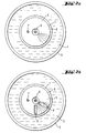
- FIGS. 2a and 2b show that the Surface of the initial cone not completely from Shielding part must be covered. Protrudes in the representation Edge area 8 of the initial cone over the edge of the Shielding part 5 out. However, it is also possible to To choose a larger diameter of the shielding part, so that from the perspective shown also the edge area 8 from Shielding part 5 appears covered. That in Figure 2b shielding part 5 shown additionally has two viewing slots 9 in the form of cutouts. Such viewing slits are provided to the visible when pulling the single crystal Observe part of the crystallization limit and the current one To be able to control the diameter of the single crystal.
- viewing slots there are two viewing slots, one can be used for Observation using one camera and the second for Observation used by the operator of the drawing system become.
- Another advantage of viewing slots is that Shielding part already at the start of pulling the initial cone can be brought into the intended position. Without Viewing slots it may be necessary for the shielding part only gradually towards the growing Initial cone must be moved because a certain one first The minimum distance above the initial cone must be observed to pass the edge of the shielding part To be able to see the crystallization limit.
- the shielding parts shown are only preferred embodiments. It is clear that the initial cone with the same effect also by a differently shaped shielding part can be covered, which can also consist of two or more individual parts.
Landscapes
- Chemical & Material Sciences (AREA)
- Engineering & Computer Science (AREA)
- Crystallography & Structural Chemistry (AREA)
- Materials Engineering (AREA)
- Metallurgy (AREA)
- Organic Chemistry (AREA)
- Crystals, And After-Treatments Of Crystals (AREA)
- Liquid Deposition Of Substances Of Which Semiconductor Devices Are Composed (AREA)
Applications Claiming Priority (2)
| Application Number | Priority Date | Filing Date | Title |
|---|---|---|---|
| DE19546987 | 1995-12-15 | ||
| DE19546987A DE19546987A1 (de) | 1995-12-15 | 1995-12-15 | Verfahren und Vorrichtung zum Ziehen eines Einkristalls |
Publications (2)
| Publication Number | Publication Date |
|---|---|
| EP0783046A1 EP0783046A1 (de) | 1997-07-09 |
| EP0783046B1 true EP0783046B1 (de) | 1999-07-28 |
Family
ID=7780294
Family Applications (1)
| Application Number | Title | Priority Date | Filing Date |
|---|---|---|---|
| EP96119963A Expired - Lifetime EP0783046B1 (de) | 1995-12-15 | 1996-12-12 | Verfahren und Vorrichtung zum Ziehen eines Einkristalls |
Country Status (6)
| Country | Link |
|---|---|
| US (2) | US5759261A (ko) |
| EP (1) | EP0783046B1 (ko) |
| JP (1) | JP3167282B2 (ko) |
| KR (1) | KR100211897B1 (ko) |
| DE (2) | DE19546987A1 (ko) |
| TW (1) | TW496911B (ko) |
Families Citing this family (4)
| Publication number | Priority date | Publication date | Assignee | Title |
|---|---|---|---|---|
| JP3428626B2 (ja) * | 1998-06-25 | 2003-07-22 | 三菱住友シリコン株式会社 | シリコン単結晶の引上げ装置及びその引上げ方法 |
| US6183556B1 (en) * | 1998-10-06 | 2001-02-06 | Seh-America, Inc. | Insulating and warming shield for a seed crystal and seed chuck |
| KR101680217B1 (ko) * | 2014-08-05 | 2016-11-28 | 주식회사 엘지실트론 | 실리콘 단결정 성장 장치 및 이를 이용한 실리콘 단결정 성장 방법 |
| JP6528178B2 (ja) * | 2015-07-31 | 2019-06-12 | 株式会社Sumco | シリコン単結晶の製造方法 |
Family Cites Families (9)
| Publication number | Priority date | Publication date | Assignee | Title |
|---|---|---|---|---|
| FR1420234A (fr) * | 1965-01-11 | 1965-12-03 | Siemens Ag | Creuset de quartz pour la fusion du silicium |
| US4078897A (en) * | 1975-04-11 | 1978-03-14 | Leybold-Heraeus Gmbh & Co. Kg | Apparatus for producing monocrystals |
| JPS56134376A (en) * | 1980-03-25 | 1981-10-21 | Marantz Japan Inc | Modulation system of automatic piano playing device |
| JPS606916B2 (ja) * | 1982-09-28 | 1985-02-21 | 工業技術院長 | 化合物半導体単結晶の製造方法 |
| JPS63147891A (ja) * | 1986-12-09 | 1988-06-20 | Sumitomo Electric Ind Ltd | 単結晶の育成方法とその装置 |
| JP2795036B2 (ja) * | 1992-02-04 | 1998-09-10 | 信越半導体株式会社 | 単結晶引上装置 |
| JPH05221786A (ja) * | 1992-02-13 | 1993-08-31 | Nippon Steel Corp | シリコン単結晶製造装置および製造方法 |
| JPH05294783A (ja) * | 1992-04-15 | 1993-11-09 | Kawasaki Steel Corp | シリコン単結晶の製造装置 |
| DE4442829A1 (de) * | 1994-12-01 | 1996-06-05 | Wacker Siltronic Halbleitermat | Vorrichtung und Verfahren zur Herstellung eines Einkristalls |
-
1995
- 1995-12-15 DE DE19546987A patent/DE19546987A1/de not_active Withdrawn
-
1996
- 1996-11-06 US US08/744,544 patent/US5759261A/en not_active Expired - Lifetime
- 1996-12-09 TW TW085115227A patent/TW496911B/zh not_active IP Right Cessation
- 1996-12-10 JP JP32986896A patent/JP3167282B2/ja not_active Expired - Fee Related
- 1996-12-12 EP EP96119963A patent/EP0783046B1/de not_active Expired - Lifetime
- 1996-12-12 DE DE59602540T patent/DE59602540D1/de not_active Expired - Lifetime
- 1996-12-13 KR KR1019960065196A patent/KR100211897B1/ko not_active Expired - Fee Related
-
1998
- 1998-03-13 US US09/039,068 patent/US6015460A/en not_active Expired - Lifetime
Also Published As
| Publication number | Publication date |
|---|---|
| TW496911B (en) | 2002-08-01 |
| DE19546987A1 (de) | 1997-06-19 |
| DE59602540D1 (de) | 1999-09-02 |
| US6015460A (en) | 2000-01-18 |
| US5759261A (en) | 1998-06-02 |
| KR100211897B1 (ko) | 1999-08-02 |
| EP0783046A1 (de) | 1997-07-09 |
| JPH09227272A (ja) | 1997-09-02 |
| KR970043345A (ko) | 1997-07-26 |
| JP3167282B2 (ja) | 2001-05-21 |
Similar Documents
| Publication | Publication Date | Title |
|---|---|---|
| DE69802707T2 (de) | Hitzeschild für eine kristallziehungsvorrichtung | |
| DE19700516B4 (de) | Einkristall-Ziehvorrichtung | |
| DE69204198T2 (de) | Czochralsky-Verfahren unter Verwendung eines Bauelementes zum Abschirmen der Strahlung der Rohmaterial-Schmelzlösung und Vorrichtung hierfür. | |
| DE19711922A1 (de) | Vorrichtung und Verfahren zum Ziehen eines Einkristalls | |
| DE112014003795B4 (de) | Silizium-Einkristall-Ziehvorrichtung | |
| DE112016003796T5 (de) | Vorrichtung zum Ziehen eines Einkristalls und Verfahren zum Ziehen eines Einkristalls | |
| DE112008000034T5 (de) | Verfahren zum Herstellen eines Einkristalls | |
| DE2942057A1 (de) | Verfahren und vorrichtung zur herstellung eines einkristall-siliziumstabs | |
| EP3997259B1 (de) | Verfahren zum ziehen eines einkristalls aus silizium gemäss der czochralski-methode | |
| DE112013006489T5 (de) | Einkristallblock, Vorrichtung und Verfahren zur Herstellung desselben | |
| EP0715005A1 (de) | Vorrichtung und Verfahren zur Herstellung eines Einkristalls | |
| DE1051806B (de) | Verfahren und Vorrichtung zum Aufwaertsziehen von Einkristallen aus einer Schmelze | |
| DE1769860A1 (de) | Vorrichtung zum Ziehen von versetzungsfreien Halbleitereinkristallstaeben | |
| DE112016004171T5 (de) | Einkristall-Herstellvorrichtung und Verfahren zum Steuern einer Schmelzenoberflächen-Position | |
| DE19546987A1 (de) | Verfahren und Vorrichtung zum Ziehen eines Einkristalls | |
| DE10143231A1 (de) | Einkristalliner Siliziumwafer, Rohling und Herstellungsverfahren derselben | |
| DE102016211614A1 (de) | Verfahren und Vorrichtung zur Herstellung von beschichteten Halbleiterscheiben | |
| DE2227883C2 (de) | Flüssigphasenepitaxieverfahren | |
| DE112008000074B4 (de) | Dotierungsvorrichtung und Verfahren zum Herstellen eines Siliziumeinkristalls | |
| DE2114645C3 (de) | Verfahren zum epitaktischen Aufwachsen einer Halbleiterverbindung | |
| DE19526711A1 (de) | Verfahren zur Bearbeitung von Siliciumwafern | |
| DE19911755B4 (de) | Vorrichtung zum Ziehen eines Halbleiterkristalls und Verfahren zum Ziehen | |
| DE2323211A1 (de) | Verfahren zur herstellung einer intermetallischen einkristall-halbleiterverbindung | |
| EP0000123A1 (de) | Verfahren zum Abscheiden einkristalliner Schichten nach der Flüssigphasen-Schiebeepitaxie. | |
| DE69110029T2 (de) | Vorrichtung zur Herstellung von Halbleitern und Verfahren zur Kontrolle der thermischen Behandlung von Wafers. |
Legal Events
| Date | Code | Title | Description |
|---|---|---|---|
| PUAI | Public reference made under article 153(3) epc to a published international application that has entered the european phase |
Free format text: ORIGINAL CODE: 0009012 |
|
| 17P | Request for examination filed |
Effective date: 19961212 |
|
| AK | Designated contracting states |
Kind code of ref document: A1 Designated state(s): DE GB IT |
|
| GRAG | Despatch of communication of intention to grant |
Free format text: ORIGINAL CODE: EPIDOS AGRA |
|
| GRAG | Despatch of communication of intention to grant |
Free format text: ORIGINAL CODE: EPIDOS AGRA |
|
| GRAH | Despatch of communication of intention to grant a patent |
Free format text: ORIGINAL CODE: EPIDOS IGRA |
|
| GRAH | Despatch of communication of intention to grant a patent |
Free format text: ORIGINAL CODE: EPIDOS IGRA |
|
| GRAA | (expected) grant |
Free format text: ORIGINAL CODE: 0009210 |
|
| AK | Designated contracting states |
Kind code of ref document: B1 Designated state(s): DE GB IT |
|
| REF | Corresponds to: |
Ref document number: 59602540 Country of ref document: DE Date of ref document: 19990902 |
|
| ITF | It: translation for a ep patent filed | ||
| GBT | Gb: translation of ep patent filed (gb section 77(6)(a)/1977) |
Effective date: 19990826 |
|
| PLBE | No opposition filed within time limit |
Free format text: ORIGINAL CODE: 0009261 |
|
| STAA | Information on the status of an ep patent application or granted ep patent |
Free format text: STATUS: NO OPPOSITION FILED WITHIN TIME LIMIT |
|
| 26N | No opposition filed | ||
| PGFP | Annual fee paid to national office [announced via postgrant information from national office to epo] |
Ref country code: GB Payment date: 20011122 Year of fee payment: 6 |
|
| REG | Reference to a national code |
Ref country code: GB Ref legal event code: IF02 |
|
| PG25 | Lapsed in a contracting state [announced via postgrant information from national office to epo] |
Ref country code: GB Free format text: LAPSE BECAUSE OF NON-PAYMENT OF DUE FEES Effective date: 20021212 |
|
| GBPC | Gb: european patent ceased through non-payment of renewal fee | ||
| PG25 | Lapsed in a contracting state [announced via postgrant information from national office to epo] |
Ref country code: IT Free format text: LAPSE BECAUSE OF NON-PAYMENT OF DUE FEES;WARNING: LAPSES OF ITALIAN PATENTS WITH EFFECTIVE DATE BEFORE 2007 MAY HAVE OCCURRED AT ANY TIME BEFORE 2007. THE CORRECT EFFECTIVE DATE MAY BE DIFFERENT FROM THE ONE RECORDED. Effective date: 20051212 |
|
| PGFP | Annual fee paid to national office [announced via postgrant information from national office to epo] |
Ref country code: DE Payment date: 20121220 Year of fee payment: 17 |
|
| REG | Reference to a national code |
Ref country code: DE Ref legal event code: R119 Ref document number: 59602540 Country of ref document: DE |
|
| REG | Reference to a national code |
Ref country code: DE Ref legal event code: R119 Ref document number: 59602540 Country of ref document: DE Effective date: 20140701 |
|
| PG25 | Lapsed in a contracting state [announced via postgrant information from national office to epo] |
Ref country code: DE Free format text: LAPSE BECAUSE OF NON-PAYMENT OF DUE FEES Effective date: 20140701 |