EP0779632A1 - Multilayer structure and sensor and fabrication process - Google Patents
Multilayer structure and sensor and fabrication process Download PDFInfo
- Publication number
- EP0779632A1 EP0779632A1 EP96402718A EP96402718A EP0779632A1 EP 0779632 A1 EP0779632 A1 EP 0779632A1 EP 96402718 A EP96402718 A EP 96402718A EP 96402718 A EP96402718 A EP 96402718A EP 0779632 A1 EP0779632 A1 EP 0779632A1
- Authority
- EP
- European Patent Office
- Prior art keywords
- layers
- type
- structure according
- magnetic structure
- layer
- Prior art date
- Legal status (The legal status is an assumption and is not a legal conclusion. Google has not performed a legal analysis and makes no representation as to the accuracy of the status listed.)
- Granted
Links
Images


Classifications
-
- G—PHYSICS
- G01—MEASURING; TESTING
- G01R—MEASURING ELECTRIC VARIABLES; MEASURING MAGNETIC VARIABLES
- G01R15/00—Details of measuring arrangements of the types provided for in groups G01R17/00 - G01R29/00, G01R33/00 - G01R33/26 or G01R35/00
- G01R15/14—Adaptations providing voltage or current isolation, e.g. for high-voltage or high-current networks
- G01R15/20—Adaptations providing voltage or current isolation, e.g. for high-voltage or high-current networks using galvano-magnetic devices, e.g. Hall-effect devices, i.e. measuring a magnetic field via the interaction between a current and a magnetic field, e.g. magneto resistive or Hall effect devices
- G01R15/205—Adaptations providing voltage or current isolation, e.g. for high-voltage or high-current networks using galvano-magnetic devices, e.g. Hall-effect devices, i.e. measuring a magnetic field via the interaction between a current and a magnetic field, e.g. magneto resistive or Hall effect devices using magneto-resistance devices, e.g. field plates
-
- B—PERFORMING OPERATIONS; TRANSPORTING
- B82—NANOTECHNOLOGY
- B82Y—SPECIFIC USES OR APPLICATIONS OF NANOSTRUCTURES; MEASUREMENT OR ANALYSIS OF NANOSTRUCTURES; MANUFACTURE OR TREATMENT OF NANOSTRUCTURES
- B82Y10/00—Nanotechnology for information processing, storage or transmission, e.g. quantum computing or single electron logic
-
- B—PERFORMING OPERATIONS; TRANSPORTING
- B82—NANOTECHNOLOGY
- B82Y—SPECIFIC USES OR APPLICATIONS OF NANOSTRUCTURES; MEASUREMENT OR ANALYSIS OF NANOSTRUCTURES; MANUFACTURE OR TREATMENT OF NANOSTRUCTURES
- B82Y25/00—Nanomagnetism, e.g. magnetoimpedance, anisotropic magnetoresistance, giant magnetoresistance or tunneling magnetoresistance
-
- G—PHYSICS
- G01—MEASURING; TESTING
- G01R—MEASURING ELECTRIC VARIABLES; MEASURING MAGNETIC VARIABLES
- G01R33/00—Arrangements or instruments for measuring magnetic variables
- G01R33/02—Measuring direction or magnitude of magnetic fields or magnetic flux
- G01R33/06—Measuring direction or magnitude of magnetic fields or magnetic flux using galvano-magnetic devices
- G01R33/09—Magnetoresistive devices
- G01R33/093—Magnetoresistive devices using multilayer structures, e.g. giant magnetoresistance sensors
-
- G—PHYSICS
- G11—INFORMATION STORAGE
- G11B—INFORMATION STORAGE BASED ON RELATIVE MOVEMENT BETWEEN RECORD CARRIER AND TRANSDUCER
- G11B5/00—Recording by magnetisation or demagnetisation of a record carrier; Reproducing by magnetic means; Record carriers therefor
- G11B5/127—Structure or manufacture of heads, e.g. inductive
- G11B5/33—Structure or manufacture of flux-sensitive heads, i.e. for reproduction only; Combination of such heads with means for recording or erasing only
- G11B5/39—Structure or manufacture of flux-sensitive heads, i.e. for reproduction only; Combination of such heads with means for recording or erasing only using magneto-resistive devices or effects
- G11B5/3903—Structure or manufacture of flux-sensitive heads, i.e. for reproduction only; Combination of such heads with means for recording or erasing only using magneto-resistive devices or effects using magnetic thin film layers or their effects, the films being part of integrated structures
-
- H—ELECTRICITY
- H01—ELECTRIC ELEMENTS
- H01F—MAGNETS; INDUCTANCES; TRANSFORMERS; SELECTION OF MATERIALS FOR THEIR MAGNETIC PROPERTIES
- H01F10/00—Thin magnetic films, e.g. of one-domain structure
- H01F10/32—Spin-exchange-coupled multilayers, e.g. nanostructured superlattices
- H01F10/324—Exchange coupling of magnetic film pairs via a very thin non-magnetic spacer, e.g. by exchange with conduction electrons of the spacer
- H01F10/325—Exchange coupling of magnetic film pairs via a very thin non-magnetic spacer, e.g. by exchange with conduction electrons of the spacer the spacer being noble metal
-
- H—ELECTRICITY
- H10—SEMICONDUCTOR DEVICES; ELECTRIC SOLID-STATE DEVICES NOT OTHERWISE PROVIDED FOR
- H10N—ELECTRIC SOLID-STATE DEVICES NOT OTHERWISE PROVIDED FOR
- H10N50/00—Galvanomagnetic devices
- H10N50/80—Constructional details
- H10N50/85—Magnetic active materials
-
- G—PHYSICS
- G11—INFORMATION STORAGE
- G11B—INFORMATION STORAGE BASED ON RELATIVE MOVEMENT BETWEEN RECORD CARRIER AND TRANSDUCER
- G11B5/00—Recording by magnetisation or demagnetisation of a record carrier; Reproducing by magnetic means; Record carriers therefor
- G11B5/127—Structure or manufacture of heads, e.g. inductive
- G11B5/33—Structure or manufacture of flux-sensitive heads, i.e. for reproduction only; Combination of such heads with means for recording or erasing only
- G11B5/39—Structure or manufacture of flux-sensitive heads, i.e. for reproduction only; Combination of such heads with means for recording or erasing only using magneto-resistive devices or effects
- G11B2005/3996—Structure or manufacture of flux-sensitive heads, i.e. for reproduction only; Combination of such heads with means for recording or erasing only using magneto-resistive devices or effects large or giant magnetoresistive effects [GMR], e.g. as generated in spin-valve [SV] devices
-
- Y—GENERAL TAGGING OF NEW TECHNOLOGICAL DEVELOPMENTS; GENERAL TAGGING OF CROSS-SECTIONAL TECHNOLOGIES SPANNING OVER SEVERAL SECTIONS OF THE IPC; TECHNICAL SUBJECTS COVERED BY FORMER USPC CROSS-REFERENCE ART COLLECTIONS [XRACs] AND DIGESTS
- Y10—TECHNICAL SUBJECTS COVERED BY FORMER USPC
- Y10T—TECHNICAL SUBJECTS COVERED BY FORMER US CLASSIFICATION
- Y10T428/00—Stock material or miscellaneous articles
- Y10T428/11—Magnetic recording head
- Y10T428/1107—Magnetoresistive
- Y10T428/1121—Multilayer
- Y10T428/1129—Super lattice [e.g., giant magneto resistance [GMR] or colossal magneto resistance [CMR], etc.]
-
- Y—GENERAL TAGGING OF NEW TECHNOLOGICAL DEVELOPMENTS; GENERAL TAGGING OF CROSS-SECTIONAL TECHNOLOGIES SPANNING OVER SEVERAL SECTIONS OF THE IPC; TECHNICAL SUBJECTS COVERED BY FORMER USPC CROSS-REFERENCE ART COLLECTIONS [XRACs] AND DIGESTS
- Y10—TECHNICAL SUBJECTS COVERED BY FORMER USPC
- Y10T—TECHNICAL SUBJECTS COVERED BY FORMER US CLASSIFICATION
- Y10T428/00—Stock material or miscellaneous articles
- Y10T428/11—Magnetic recording head
- Y10T428/115—Magnetic layer composition
-
- Y—GENERAL TAGGING OF NEW TECHNOLOGICAL DEVELOPMENTS; GENERAL TAGGING OF CROSS-SECTIONAL TECHNOLOGIES SPANNING OVER SEVERAL SECTIONS OF THE IPC; TECHNICAL SUBJECTS COVERED BY FORMER USPC CROSS-REFERENCE ART COLLECTIONS [XRACs] AND DIGESTS
- Y10—TECHNICAL SUBJECTS COVERED BY FORMER USPC
- Y10T—TECHNICAL SUBJECTS COVERED BY FORMER US CLASSIFICATION
- Y10T428/00—Stock material or miscellaneous articles
- Y10T428/12—All metal or with adjacent metals
- Y10T428/12465—All metal or with adjacent metals having magnetic properties, or preformed fiber orientation coordinate with shape
-
- Y—GENERAL TAGGING OF NEW TECHNOLOGICAL DEVELOPMENTS; GENERAL TAGGING OF CROSS-SECTIONAL TECHNOLOGIES SPANNING OVER SEVERAL SECTIONS OF THE IPC; TECHNICAL SUBJECTS COVERED BY FORMER USPC CROSS-REFERENCE ART COLLECTIONS [XRACs] AND DIGESTS
- Y10—TECHNICAL SUBJECTS COVERED BY FORMER USPC
- Y10T—TECHNICAL SUBJECTS COVERED BY FORMER US CLASSIFICATION
- Y10T428/00—Stock material or miscellaneous articles
- Y10T428/12—All metal or with adjacent metals
- Y10T428/12493—Composite; i.e., plural, adjacent, spatially distinct metal components [e.g., layers, joint, etc.]
- Y10T428/12771—Transition metal-base component
- Y10T428/12806—Refractory [Group IVB, VB, or VIB] metal-base component
-
- Y—GENERAL TAGGING OF NEW TECHNOLOGICAL DEVELOPMENTS; GENERAL TAGGING OF CROSS-SECTIONAL TECHNOLOGIES SPANNING OVER SEVERAL SECTIONS OF THE IPC; TECHNICAL SUBJECTS COVERED BY FORMER USPC CROSS-REFERENCE ART COLLECTIONS [XRACs] AND DIGESTS
- Y10—TECHNICAL SUBJECTS COVERED BY FORMER USPC
- Y10T—TECHNICAL SUBJECTS COVERED BY FORMER US CLASSIFICATION
- Y10T428/00—Stock material or miscellaneous articles
- Y10T428/12—All metal or with adjacent metals
- Y10T428/12493—Composite; i.e., plural, adjacent, spatially distinct metal components [e.g., layers, joint, etc.]
- Y10T428/12771—Transition metal-base component
- Y10T428/12861—Group VIII or IB metal-base component
- Y10T428/12896—Ag-base component
-
- Y—GENERAL TAGGING OF NEW TECHNOLOGICAL DEVELOPMENTS; GENERAL TAGGING OF CROSS-SECTIONAL TECHNOLOGIES SPANNING OVER SEVERAL SECTIONS OF THE IPC; TECHNICAL SUBJECTS COVERED BY FORMER USPC CROSS-REFERENCE ART COLLECTIONS [XRACs] AND DIGESTS
- Y10—TECHNICAL SUBJECTS COVERED BY FORMER USPC
- Y10T—TECHNICAL SUBJECTS COVERED BY FORMER US CLASSIFICATION
- Y10T428/00—Stock material or miscellaneous articles
- Y10T428/12—All metal or with adjacent metals
- Y10T428/12493—Composite; i.e., plural, adjacent, spatially distinct metal components [e.g., layers, joint, etc.]
- Y10T428/12771—Transition metal-base component
- Y10T428/12861—Group VIII or IB metal-base component
- Y10T428/12903—Cu-base component
- Y10T428/1291—Next to Co-, Cu-, or Ni-base component
-
- Y—GENERAL TAGGING OF NEW TECHNOLOGICAL DEVELOPMENTS; GENERAL TAGGING OF CROSS-SECTIONAL TECHNOLOGIES SPANNING OVER SEVERAL SECTIONS OF THE IPC; TECHNICAL SUBJECTS COVERED BY FORMER USPC CROSS-REFERENCE ART COLLECTIONS [XRACs] AND DIGESTS
- Y10—TECHNICAL SUBJECTS COVERED BY FORMER USPC
- Y10T—TECHNICAL SUBJECTS COVERED BY FORMER US CLASSIFICATION
- Y10T428/00—Stock material or miscellaneous articles
- Y10T428/26—Web or sheet containing structurally defined element or component, the element or component having a specified physical dimension
- Y10T428/263—Coating layer not in excess of 5 mils thick or equivalent
- Y10T428/264—Up to 3 mils
- Y10T428/265—1 mil or less
Definitions
- the present invention relates generally to magnetic field or flux detectors, and more particularly to magnetoresistive sensors. These are for example used in magnetic recording, to read the information written on a magnetic information storage medium. More generally, the type of microsensor described in the present invention relates to the detection of weak magnetic fields (typically in the range 0.1 Oe to a few 10 Oe, i.e. from a few A / m to a few thousand A / m). As other examples of application, there may be mentioned the determination of the electric current flowing in a conductor from the measurement of the magnetic field prevailing in the vicinity of this conductor, the position sensors (translation or rotation) or the magnetoresistive compasses.
- weak magnetic fields typically in the range 0.1 Oe to a few 10 Oe, i.e. from a few A / m to a few thousand A / m.
- the determination of the electric current flowing in a conductor from the measurement of the magnetic field prevailing in the vicinity of this conductor, the position sensors (translation or rotation
- magnetoresistive sensors used for the detection of weak magnetic fields were based on the anisotropy effect of magnetoresistance.
- a detailed description of this effect can be found in the article by DA Thompson et al., IEEE Trans. Mag. Mag-11, p. 1039 (1975).
- This effect present in ferromagnetic transition metals (alloys based on Ni, Co, Fe), consists in a variation of the resistivity of the magnetic material in function of the angle between the measurement current flowing in the magnetoresistive element and the magnetization of the material.
- the relative change in resistivity of the magnetic material can reach 4 to 5% at room temperature, in fields of the order of kA / m, in massive ferromagnetic transition metals. This amplitude is nevertheless reduced to 1 or 2%, when the same materials are deposited in thin layers of the order of 15 to 30 nanometers thick. This thickness range is that used in current magnetoresistive sensors. The sensitivity of these sensors is therefore limited. Furthermore, their response is not linear because the variation in resistivity is proportional to the square of the cosine of the angle between the current and the magnetization.
- Patent FR-2 698 965 entitled “multilayer magnetic structure and sensor with high magnetoresistance, and process for manufacturing the structure” describes a particular multilayer system, based on alternating layers of Permalloy (alloy based on Ni and Fe, with a composition close to Ni 80 Fe 20 ) with a thickness of the order of 1 to 2 nm, and of Ag (with a thickness of 1 to 2 nm). For this thickness of Ag, an antiferromagnetic coupling exists between the layers of Permalloy through the layers of Ag.
- this material is prepared by sputtering while keeping the substrate in the process of being deposited at low temperature (liquid nitrogen), it then has very good magnetic and magnetoresistive structural properties, which make it particularly promising for applications.
- this material offers a good sensitivity in terms of slope of relative variation of resistance R, according to the field H to be measured of the order of 0.1 to 0.2% / Oe), good linearity of the response over a wide range of fields to be measured (of the order of 1 to a few tens of Oe).
- this material offers good thermal stability up to temperatures of the order of 250 ° C due to the immiscibility of NiFe and Ag. However, the properties of the material deteriorate if annealing is carried out at temperatures above 250 ° C.
- the object of the present invention is to improve the thermal stability of the multilayer material and to ensure that it retains properties that are as good, or even better, after exposure to temperatures up to 300 ° C, than in the raw state of deposition.
- the problem to which the present invention responds is therefore to increase as much as possible the thermal stability of the magnetoresistive material constituting the magnetoresistive sensors, while retaining a good sensitivity of the material in weak fields.
- the increase in thermal stability also ensures better longevity of the material, and in particular better resistance to electromigration.
- the introduction of the interfacial layer has the effect of greatly increasing the structural stability of the material when the latter is subjected to anneals which can go up to 300 ° C. for 20 minutes.
- a comparison of the effect of annealing at 300 ° C for 20 minutes, on a multilayer of composition (NiFe 2.5 nm / Ag 1.1 nm) 20 and (Co 0.2 nm / NiFe 2.5 nm / Co 0.2 nm / Ag 1.1 nm) 20 shows that the magnetoresistive properties of the first structure (without Co at the interfaces) deteriorated a lot during the annealing while the magnetoresistive properties of the second were preserved.
- the amplitude of magnetoresistance is also increased by the addition of the thin layer of Co to the interfaces.
- a doubling of the magnetoresistance amplitude is observed in the composition of structures (NiFe 2.5 nm / Ag 1.1 nm) 10 by the addition of 0.25 nm of Co at the interfaces.
- the stack comprises at least two layers of the first type and one layer of the second type.
- a layer of Co can also be introduced on either side of the stack.
- the stack can comprise different layers of the first type and / or different layers of the second type.
- layer based on magnetic materials is meant a layer corresponding to the generic formula: Ni 100-xyz CO x Fe y A z where 0 ⁇ x ⁇ 100, 0 ⁇ y ⁇ 100 and o ⁇ z ⁇ 40, and 0 ⁇ x + y + z ⁇ 100 and A denotes any element or set of elements.
- materials corresponding to this formula include: permalloy, mu-metal, supermalloy, sundust, ...
- An alloy rich in silver, for the layers of the second type, can be of the formula Ag x Cu 1-x or Ag x Au 1-x with o ⁇ x ⁇ 0.5.
- pure silver will give the best thermal stability, but the addition of copper or even more surely, gold, would reduce the saturation field of the device and therefore increase its sensitivity.
- the interfacial layer has a thickness of between a fraction of the atomic plane and a few atomic planes.
- the thickness of the layers of the second type can be such that an antiferromagnetic coupling exists between the layers of the first type through the layers of the second type and the interfacial layers.
- the thickness of the layers of the second type can for example be between 0.8 and 1.5 nm.
- the layer of the second type can be of a thickness such that there is no, or only a very small, antiferromagnetic coupling between the layers of the first type.
- the layers can be deposited by condensation of metallic vapors on a substrate, at a temperature below ambient temperature.
- the deposition can for example be carried out by sputtering.
- the invention also relates to a multilayer sensor with magnetoresistive effect comprising a layered magnetic structure as described above.
- the invention also relates to a current sensor intended to measure the current flowing through an electrical conductor comprising a magnetoresistive tape surrounding the conductor and the ends of which are intended to be connected to a current measuring device, the tape being made up in a layered magnetic structure as described above.
- a first example of a structure according to the invention has the composition: substrate / buffer layer / (Py ep y / X e x / (Ag e Ag / X e x / Py ep y / X e x ) n / Ag e Ag / X e x / Py ep y / cover layer.
- FIG. 1 Such a structure is shown diagrammatically in FIG. 1 where the references 2 and 4 respectively designate the substrate and the layer buffer. References 6 and 8 respectively designate a first layer Py and a layer X also called the interfacial layer.
- the set Ag / X / Py / X is generally designated by the reference 10. This set or this pattern can be repeated n times.
- the references 12, 14 and 16 respectively designate a last layer of silver, an interfacial layer X and a last layer Py on which a covering layer 18 is deposited.
- the substrate 2 can be for example intrinsic or weakly doped Si (so that it is not too conductive with respect to the multilayer, and therefore that it does not shunt the current), glass, Kapton, an oxide such as MgO ...
- the purpose of buffer layer 4 is to improve the structural quality of the material during its growth. It can be, for example, in Tantalum with a thickness of a few nanometers (5 nm for example).
- Py denotes an alloy from the family of alloys of composition Ni 100-xyz Co x Fe y A z and preferably an alloy of the Permalloy or mu-metal type.
- Permalloy and mu-metal exist with a composition close to Ni 80 Fe 20 with the possibility of adding a third or fourth element such as Co or Mo.
- Most of these materials are characterized by soft magnetic properties (low hysteresis (field coercive of the order of a few Oe or less), low saturation field (ten Oe (800 A / m) or less), high permeability (several hundred), and can enter the proposed structure.
- Ni 100-xyz Co x Fe y A z , x + y + z is preferably between 0 and 40, x between 0 and 30, y between 0 and 30, z between 0 and 20.
- A denotes a single element or several elements, such as for example Cu, Cr, Mo, V, B which are sometimes added as additives in small quantities in the composition high permeability alloys (Permalloy, mu-metal, Supermalloy ). Examples of these alloys are given in "Introduction to magnetic materials, Cullity, Addison-Wesley Publishing Company, 1972, p. 529, table 13.6).
- ep y is the thickness of these layers of Permalloy (for example layers 8, 16 in FIG. 1). It can vary between 1 and 20 nm and it is preferably between 1.5 and 5 nm. Indeed, these thicknesses must be of the order of magnitude or less than the mean electronic free paths in these materials (which are of the order of ten nm). In addition, the maximum magnetoresistance is observed around a thickness of Py of 2.2 nm, the best sensitivity is obtained for thicknesses greater than 6 nm while the thermal stability degrades from approximately 5 nm. This is why the thickness of Py will preferably be between 1.5 and 5 nm.
- X denotes the thin interfacial layer introduced at the interfaces between the Permalloy and the Ag (for example: layers 8 and 14 in FIG. 1).
- X can be Co or an alloy rich in Co (for example Co 90 Fe 10 or Co 70 Fe 30 ).
- e X is the thickness of this interfacial layer. It can vary from a fraction of the atomic plane to a few atomic planes (for example: 2, 3 or 4 planes) and it is preferably around an atomic plane (0.25 nm).
- Figures 3B and 3C show that an atomic plane of Co is sufficient to obtain a consequent increase in giant magnetoresistance and thermal stability. Putting more than one atomic plane of Co tends to increase the field of saturation relatively appreciably and therefore to reduce the sensitivity of the material.
- e Ag denotes the thickness of the silver layers. This thickness is preferably such that an antiferromagnetic coupling exists between the layers of Permalloy through the layers of Ag. This condition is satisfied for thicknesses of Ag of between 0.9 and 1.3 nm approximately.
- n denotes the number of periods of the multilayer without counting the external Py layers (n can vary from 0 to any integer value, but is typically between 0 and 50 for applications in magnetic recording).
- the cover layer 18 serves to prevent oxidation of the structure. It can be in Ta for example.
- Another example of structure according to the invention is of the “spin valve” type based on Ag.
- the simple spin valve structures of the NiFe (6 to 8 nm) / Cu (2 to 4 nm) / NiFe (3 to 6 nm) / FeMn (7 to 12 nm) type exhibit magnetoresistive properties which are quite interesting for applications. in the magnetic recording.
- dual spin valves such as NiO (5 to 10 nm) / NiFe (3 to 6 nm) / Cu (2 to 4 nm) / NiFe (6 to 8 nm) / Cu (2 to 4 nm) / NiFe (3 to 6 nm) / FeMn (7 to 12 nm).
- the invention therefore also relates to a spin valve structure having as composition: substrate / buffer layer / Py (5 to 10 nm) / X e X / Ag (2 to 4 nm) / X e X / Py (3 to 6 nm ) / antiferromagnetic layer (for example FeMn 7 at 12 nm) / cover layer.
- the substrate, the buffer layer, the covering layer, the thin interfacial layer have the same characteristics as described for the first proposed structure.
- the purpose of the antiferromagnetic layer is to trap the magnetization of the adjacent Py layer by exchange anisotropy.
- a third structure according to the invention is a dual spin valve, having the composition: substrate / buffer layer / antiferromagnetic layer (for example NiO from 5 to 10 nm) / NiFe (3 to 6 nm) / X e X / Ag (2 to 4 nm) / X e X / NiFe (6 to 8 nm) / X e X / Ag (2 to 4 nm) / X e X / NiFe (3 to 6 nm) / antiferromagnetic layer (for example FeMn from 7 to 12 nm) / cover layer.
- substrate / buffer layer / antiferromagnetic layer for example NiO from 5 to 10 nm
- NiFe 3 to 6 nm
- X e X / Ag 2 to 4 nm
- X e X / Ag 2 to 4 nm
- antiferromagnetic layer for example FeMn from 7 to 12 nm
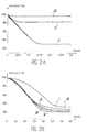
- FIGS. 2A and 2B illustrate the increase in the stability of the properties of these structures, during annealing between 250 ° C. and 300 ° C., linked to the addition of the thin interfacial layers of Co to the Py / Ag interfaces.
- FIG. 2A represents the magnetoresistance of a multilayer of composition composition Si / SiO 2 / (Ni 80 Fe 20 2.5 nm / Ag 1.1 nm) 20 deposition crude (curve I), after annealing at 275 ° C for 20 minutes (curve II) and at 290 ° C for 20 minutes (curve III).
- FIG. 2B shows the magnetoresistance of a multilayer of substrate composition Si / (Co 0.3 nm / Ni 80 Fe 20 1.9 nm / Co 0.3 nm / Ag 1.1 nm) 20 crude deposition (curve I) and after various successive anneals (curves II-V) at increasing temperatures for 20 minutes. It can be seen that, compared to the raw deposition state (curve I), the magnetoresistance increased after annealing at 275 ° C (curve V), while the saturation field decreased.
- Figure 3A shows a bundle of curves obtained for different samples corresponding to increasing thickness e Co (in nm) of the interfacial Co layers. These samples have for composition: substrate Si / SiO 2 / (Co e Co / Ni 80 Fe 20 (2,5-2e Co ) nm / Co e Co / Ag 1,1 nm) 10 .
- FIG. 3B represents the amplitude of magnetoresistance as a function of the thickness e Co of the layers of Co.
- This curve shows that the amplitude of magnetoresistance increases very quickly at small thicknesses, to practically saturate when a monoatomic layer of Co has been introduced at the interfaces.
- the introduction of an atomic plane of Co at the Permalloy / Ag interfaces is therefore sufficient to double the amplitude of magnetoresistance and to ensure better thermal stability of the structure.
- the saturation field unfortunately, also increases with the thickness of the interfacial layers of Co. This is clearly visible in FIG. 3A.
- the saturation field is plotted as a function of the thickness of Co in FIG. 3C.
- the H sat field increases a little less quickly than the amplitude of magnetoresistance as a function of the thickness of Co. It is nevertheless possible to reduce this saturation field by varying the thickness of Ag.
- FIG. 4A represents a bundle of curves R (H) R (O) . 100 obtained for different samples corresponding to increasing thickness e Ag of the layers of Ag. These samples have the composition: substrate Si / (Co 0.2 nm / Ni 80 Fe 20 2.1 nm / Co 0.2 nm / Ag e Ag ) 10 .
- a very large variation in the saturation field is observed as a function of the thickness of Ag.
- the coupling between layers of Permalloy with Co at the interfaces through Ag is antiferromagnetic for thicknesses of Ag of between approximately 0.9 nm and 1.45 nm.
- the saturation field is minimal towards the upper end of this region of thickness of Ag, that is to say around 1.3 to 1.4 nm of Ag.
- FIG. 4B represents the variations of the saturation field as a function of the thickness of Ag.
- the preferred thickness of Ag to be used to obtain the best possible sensitivity ⁇ R / R (H) is therefore of the order of 1.3 to 1.4 nm.
- the structures given as examples in this document were prepared by sputtering.
- the basic vacuum in the production enclosure was of the order of 2.10 -8 mbar.
- Argon at a pressure of 1.5.10 -3 mbar, was used as the gas for spraying.
- the NiFe target was powered by an RF source, the Co and Ag targets by DC sources.
- the substrates were cooled, during the deposition of these materials, to a temperature close to that of liquid nitrogen, to avoid the coalescence of the layers of Ag.
- Other techniques for developing thin metallic layers could be used for the preparation of these materials, such as molecular beam epitaxy or ion beam sputtering.
- a magnetic structure according to the invention can be used to produce a current sensor as described in application FR-2 710 753 (DD 1289).
- FIG. 5 represents such a current sensor 20, in the position for measuring a current I passing through an electrical conductor 22.
- the current sensor 20 in the form of a ring comprises a magnetoresistive tape 24 also in the form of a ring.
- the ends 26 and 28 of the ribbon 24 are arranged close to each other so that the ribbon forms an almost complete circle. These ends are arranged to allow the electrical connection of the strip 24 with a direct current generator i (or of voltage). Observation of the voltage v across the ribbon 24 makes it possible to note the variation in the resistance of the ribbon under the effect of the magnetic field H I induced by the current I.
- a magnetic structure according to the invention can also be used to produce a magnetic head.
- FIG. 6 shows, by way of illustration, how to implement the invention in a magnetic writing and / or reading head. Such a head has been described in French patent application No. 93 13249 filed on November 8, 1993.
- the head is shown in section.
- the magnetoresistance 50 By adjusting the current flowing in the conductor 80, the magnetoresistance 50 will be biased to an appropriate value.
- the main advantage provided by the invention is to increase the stability of the structural properties of the material during annealing at temperatures ranging from at least 250 ° C to 300 ° C, temperatures to which the material can be subjected during lithographic processes.
- the addition of thin interfacial layers of Co, or of alloys rich in Co, to the Permalloy / Ag interfaces makes it possible to increase the amplitude of magnetoresistance which, in particular in spin valve structures, leads to an increase the sensitivity of the material (increase in ⁇ R / R without significant increase in the field variation necessary to observe the entire amplitude of magnetoresistance).
Abstract
Description
La présente invention concerne globalement les détecteurs de champs ou de flux magnétiques, et plus particulièrement les capteurs magnétorésistifs. Ces derniers sont par exemple utilisés dans l'enregistrement magnétique, pour lire l'information inscrite sur un support magnétique de stockage de l'information. De façon plus générale, le type de microcapteur décrit dans la présente invention concerne la détection de faibles champs magnétiques (typiquement dans la gamme 0,1 Oe à quelques 10 Oe, c'est-à-dire de quelques A/m à quelques milliers d'A/m). Comme autres exemples d'application, on peut citer la détermination du courant électrique circulant dans un conducteurs à partir de la mesure du champ magnétique régnant dans le voisinage de ce conducteurs, les capteurs de position (translation ou rotation) ou les boussoles magnétorésistives.The present invention relates generally to magnetic field or flux detectors, and more particularly to magnetoresistive sensors. These are for example used in magnetic recording, to read the information written on a magnetic information storage medium. More generally, the type of microsensor described in the present invention relates to the detection of weak magnetic fields (typically in the range 0.1 Oe to a few 10 Oe, i.e. from a few A / m to a few thousand A / m). As other examples of application, there may be mentioned the determination of the electric current flowing in a conductor from the measurement of the magnetic field prevailing in the vicinity of this conductor, the position sensors (translation or rotation) or the magnetoresistive compasses.
Jusqu'en 1990, les capteurs magnétorésistifs utilisés pour la détection des faibles champs magnétiques, notamment dans le domaine de l'enregistrement magnétique, étaient basés sur l'effet d'anisotropie de la magnétorésistance. Une description détaillée de cet effet se trouve dans l'article de D.A. Thompson et al., IEEE Trans. Mag. Mag-11, p. 1039 (1975). Cet effet, présent dans les métaux de transition ferromagnétiques (alliages à base de Ni, Co, Fe), consiste en une variation de la résistivité du matériau magnétique en fonction de l'angle entre le courant de mesure circulant dans l'élément magnétorésistif et l'aimantation du matériau. Le changement relatif de résistivité du matériau magnétique (Δρ/ρ) peut atteindre 4 à 5% à température ambiante, dans des champs de l'ordre du kA/m, dans les métaux de transition ferromagnétiques massifs. Cette amplitude est néanmoins réduite à 1 ou 2%, lorsque les mêmes matériaux sont déposés en couches minces de l'ordre de 15 à 30 nanomètres d'épaisseur. Ce domaine d'épaisseur est celui utilisé dans les capteurs magnétorésistifs actuels. La sensibilité de ces capteurs est donc limitée. Par ailleurs, leur réponse n'est pas linéaire du fait que la variation de résistivité est proportionnelle au carré du cosinus de l'angle entre le courant et l'aimantation.Until 1990, magnetoresistive sensors used for the detection of weak magnetic fields, particularly in the field of magnetic recording, were based on the anisotropy effect of magnetoresistance. A detailed description of this effect can be found in the article by DA Thompson et al., IEEE Trans. Mag. Mag-11, p. 1039 (1975). This effect, present in ferromagnetic transition metals (alloys based on Ni, Co, Fe), consists in a variation of the resistivity of the magnetic material in function of the angle between the measurement current flowing in the magnetoresistive element and the magnetization of the material. The relative change in resistivity of the magnetic material (Δρ / ρ) can reach 4 to 5% at room temperature, in fields of the order of kA / m, in massive ferromagnetic transition metals. This amplitude is nevertheless reduced to 1 or 2%, when the same materials are deposited in thin layers of the order of 15 to 30 nanometers thick. This thickness range is that used in current magnetoresistive sensors. The sensitivity of these sensors is therefore limited. Furthermore, their response is not linear because the variation in resistivity is proportional to the square of the cosine of the angle between the current and the magnetization.
En 1989, des effets de magnétorésistance géante ont été découverts dans des multicouches (Fe 3nm/Cr 0,9nm)n et par la suite dans de nombreux autres systèmes en multicouches formés d'une alternance de couches de métal de transition ferromagnétique et de couches de métal non-magnétique. Dans ces systèmes, l'effet de magnétorésistance est essentiellement lié à un changement dans l'orientation relative des aimantations des couches ferromagnétiques successives. Cet effet est nommé dans la littérature "magnétorésistance géante" ou "effet de vanne de spin" (en anglais "giant magnetoresistance" ou "spin-valve effect"). Des revues sur ces matériaux en multicouche présentant une magnétorésistance géante ont été publiées par H. Yamamoto et T. Shinjo, IEEE Translation Journal on Magnetics in Japan, vol. 7, n°9, Sept 1992 ainsi que par B. Dieny, Journal of Magnetism and Magnetic Materials 136 ( 1994) 335.In 1989, giant magnetoresistance effects were discovered in multilayers (Fe 3nm / Cr 0.9nm) n and subsequently in many other multilayer systems formed by alternating layers of ferromagnetic transition metal and layers of non-magnetic metal. In these systems, the magnetoresistance effect is essentially linked to a change in the relative orientation of the magnetizations of the successive ferromagnetic layers. This effect is called in the literature "giant magnetoresistance" or "spin valve effect" (in English "giant magnetoresistance" or "spin-valve effect"). Reviews of these multilayer materials with giant magnetoresistance have been published by H. Yamamoto and T. Shinjo, IEEE Translation Journal on Magnetics in Japan, vol. 7, n ° 9, Sept 1992 as well as by B. Dieny, Journal of Magnetism and Magnetic Materials 136 (1994) 335.
Le brevet FR-2 698 965 intitulé "structure et capteur magnétique multicouches à forte magnétorésistance, et procédé de fabrication de la structure " décrit un système en multicouche particulier, à base de couches alternées de Permalloy (alliage à base de Ni et de Fe, de composition voisine de Ni80Fe20) d'épaisseur de l'ordre de 1 à 2 nm, et d'Ag (d'épaisseur de 1 à 2 nm). Pour cette épaisseur d'Ag, un couplage antiferromagnétique existe entre les couches de Permalloy à travers les couches d'Ag. Lorsque ce matériau est préparé par pulvérisation cathodique en maintenant le substrat en cours de dépôt à basse température (azote liquide), il présente alors de très bonne propriétés structurales magnétiques et magnétorésistives, qui le rendent particulièrement prometteur pour des applications. En effet, il offre une bonne sensibilité en terme de pente de variation relative de résistance R, en fonction du champ H à mesurer
Le problème auquel la présente invention répond est donc d'augmenter autant que possible la stabilité thermique du matériau magnétorésistif constitutif des capteurs magnétorésistifs, tout en conservant une bonne sensibilité du matériau en champs faibles. L'augmentation de la stabilité thermique assure également une meilleure longévité du matériau, et en particulier une meilleure résistance à l'électromigration.The problem to which the present invention responds is therefore to increase as much as possible the thermal stability of the magnetoresistive material constituting the magnetoresistive sensors, while retaining a good sensitivity of the material in weak fields. The increase in thermal stability also ensures better longevity of the material, and in particular better resistance to electromigration.
Ainsi, l'invention a pour objet une structure magnétique en couche comportant un empilement alterné :
- de couches d'un premier type, à base de matériaux magnétiques,
- de couches d'un second type, en Ag ou en un alliage riche en Ag,
- une couche interfaciale mince de Co ou d'un alliage riche en Co étant située aux interfaces des couches du premier type et des couches du second type.
- layers of a first type, based on magnetic materials,
- layers of a second type, made of Ag or of an alloy rich in Ag,
- a thin interfacial layer of Co or of a Co-rich alloy being situated at the interfaces of the layers of the first type and of the layers of the second type.
L'introduction de la couche interfaciale a pour effet de beaucoup augmenter la stabilité structurale du matériau lorsque celui-ci est soumis à des recuits pouvant aller jusqu'à 300°C pendant 20 minutes. Une comparaison de l'effet d'un recuit à 300°C pendant 20 minutes, sur une multicouche de composition (NiFe 2,5 nm/Ag 1,1 nm)20 et (Co 0,2 nm/NiFe 2,5 nm/ Co 0,2 nm/Ag 1,1 nm)20 montre que les propriétés magnétorésistives de la première structure (sans Co aux interfaces) se sont beaucoup dégradées au cours du recuit alors que les propriétés magnétorésistives de la seconde ont été conservées. Par ailleurs, l'amplitude de magnétorésistance est aussi augmentée par l'adjonction de la fine couche de Co aux interfaces. Un doublement de l'amplitude de magnétorésistance est observée dans des structures de composition (NiFe 2,5 nm/Ag 1,1 nm)10 par l'ajout de 0,25 nm de Co aux interfaces.The introduction of the interfacial layer has the effect of greatly increasing the structural stability of the material when the latter is subjected to anneals which can go up to 300 ° C. for 20 minutes. A comparison of the effect of annealing at 300 ° C for 20 minutes, on a multilayer of composition (NiFe 2.5 nm / Ag 1.1 nm) 20 and (Co 0.2 nm / NiFe 2.5 nm / Co 0.2 nm / Ag 1.1 nm) 20 shows that the magnetoresistive properties of the first structure (without Co at the interfaces) deteriorated a lot during the annealing while the magnetoresistive properties of the second were preserved. In addition, the amplitude of magnetoresistance is also increased by the addition of the thin layer of Co to the interfaces. A doubling of the magnetoresistance amplitude is observed in the composition of structures (NiFe 2.5 nm / Ag 1.1 nm) 10 by the addition of 0.25 nm of Co at the interfaces.
De préférence, l'empilement comporte au moins deux couches du premier type et une couche du second type.Preferably, the stack comprises at least two layers of the first type and one layer of the second type.
Par ailleurs, une couche de Co peut également être introduite de part et d'autre de l'empilement.Furthermore, a layer of Co can also be introduced on either side of the stack.
L'empilement peut comporter des couches différentes du premier type et/ou des couches différentes du second type.The stack can comprise different layers of the first type and / or different layers of the second type.
Par ailleurs, par couche à base de matériaux magnétiques on entend une couche répondant à la formule générique : Ni100-x-y-zCOxFeyAz où 0≤x≤100, 0≤y≤100 et o≤z≤40, et 0≤x+y+z≤100 et A désigne un élément ou un ensemble d'éléments quelconques. A titre d'exemple de matériaux correspondants à cette formule, on peut citer : le permalloy, le mu-métal, le supermalloy, le sundust, ...Furthermore, by layer based on magnetic materials is meant a layer corresponding to the generic formula: Ni 100-xyz CO x Fe y A z where 0≤x≤100, 0≤y≤100 and o≤z≤40, and 0≤x + y + z≤100 and A denotes any element or set of elements. Examples of materials corresponding to this formula include: permalloy, mu-metal, supermalloy, sundust, ...
Un alliage riche en argent, pour les couches du second type, peut être de formule AgxCu1-x ou AgxAu1-x avec o<x<0,5. A priori, l'argent pur donnera la meilleure stabilité thermique, mais l'adjonction de cuivre ou encore plus sûrement, d'or, permettrait de réduire le champ à saturation du dispositif et donc d'accroître sa sensibilité.An alloy rich in silver, for the layers of the second type, can be of the formula Ag x Cu 1-x or Ag x Au 1-x with o <x <0.5. A priori, pure silver will give the best thermal stability, but the addition of copper or even more surely, gold, would reduce the saturation field of the device and therefore increase its sensitivity.
De préférence, la couche interfaciale a une épaisseur comprise entre une fraction de plan atomique et quelques plans atomiques.Preferably, the interfacial layer has a thickness of between a fraction of the atomic plane and a few atomic planes.
L'épaisseur des couches du second type peut être telle qu'un couplage antiferromagnétique existe entre les couches du premier type à travers les couches du second type et les couches interfaciales. L'épaisseur des couches du second type peut être par exemple comprise entre 0,8 et 1,5 nm.The thickness of the layers of the second type can be such that an antiferromagnetic coupling exists between the layers of the first type through the layers of the second type and the interfacial layers. The thickness of the layers of the second type can for example be between 0.8 and 1.5 nm.
Selon un autre aspect, dans certaines applications, la couche du second type peut être d'une épaisseur telle qu'il n'existe aucun, ou seulement un très faible, couplage antiferromagnétique entre les couches du premier type.According to another aspect, in certain applications, the layer of the second type can be of a thickness such that there is no, or only a very small, antiferromagnetic coupling between the layers of the first type.
L'invention a également pour objet un procédé de réalisation d'une structure magnétique en couche comportant les étapes de :
- dépôt de couches d'un premier type, à base de matériaux magnétiques,
- dépôt de couches d'un second type, en Ag ou en un alliage riche en Ag,
- formation d'une couche interfaciale mince de Co ou d'un alliage riche en Co aux interfaces des couches de premier et de second types.
- deposition of layers of a first type, based on magnetic materials,
- deposition of layers of a second type, of Ag or of an alloy rich in Ag,
- formation of a thin interfacial layer of Co or of an alloy rich in Co at the interfaces of the layers of first and second types.
Les couches peuvent être déposées par condensation de vapeurs métalliques sur un substrat, à une température inférieure à la température ambiante. Le dépôt peut par exemple être réalisé par pulvérisation cathodique.The layers can be deposited by condensation of metallic vapors on a substrate, at a temperature below ambient temperature. The deposition can for example be carried out by sputtering.
L'invention a également pour objet un capteur multicouches à effet magnétorésistif comportant une structure magnétique en couche telle que décrite ci-dessus.The invention also relates to a multilayer sensor with magnetoresistive effect comprising a layered magnetic structure as described above.
Ainsi, l'invention a aussi pour objet un capteur de courant destiné à mesurer le courant parcourant un conducteur électrique comprenant un ruban magnétorésistif entourant le conducteur et dont les extrémités sont destinées à être connectées à un dispositif de mesure du courant, le ruban étant constitué en structure magnétique en couche telle que décrite ci-dessus.Thus, the invention also relates to a current sensor intended to measure the current flowing through an electrical conductor comprising a magnetoresistive tape surrounding the conductor and the ends of which are intended to be connected to a current measuring device, the tape being made up in a layered magnetic structure as described above.
De toute façon, les caractéristiques et avantages de l'invention apparaîtront mieux à la lumière de la description qui va suivre. Cette description porte sur les exemples de réalisation, donnés à titre explicatif et non limitatif, en se référant à des dessins annexés sur lesquels :
- la figure 1 représente une structure multicouche selon l'invention,
- les figures 2A et 2B représentent la magnétorésistance d'une multicouche respectivement selon l'art antérieur et selon l'invention,
- les figures 3A et 3B représentent l'évolution de la magnétorésistance en fonction de l'épaisseur de Co,
- la figure 3C représente l'évolution du champ de saturation en fonction de l'épaisseur de Co,
- les figures 4A et 4B représentent l'évolution de la magnétorésistance et du champ magnétique de saturation en fonction de l'épaisseur de la couche d'argent,
- la figure 5 représente schématiquement une application de l'invention à un capteur de courant,
- la figure 6 représente une application de l'invention à une tête magnétique d'écriture et/ou de lecture.
- FIG. 1 represents a multilayer structure according to the invention,
- FIGS. 2A and 2B represent the magnetoresistance of a multilayer respectively according to the prior art and according to the invention,
- FIGS. 3A and 3B represent the evolution of the magnetoresistance as a function of the thickness of Co,
- FIG. 3C represents the evolution of the saturation field as a function of the thickness of Co,
- FIGS. 4A and 4B represent the evolution of the magnetoresistance and of the saturation magnetic field as a function of the thickness of the silver layer,
- FIG. 5 schematically represents an application of the invention to a current sensor,
- FIG. 6 represents an application of the invention to a magnetic writing and / or reading head.
Un premier exemple de structure selon l'invention a pour composition :
substrat/couche tampon/(Py epy/X ex/(Ag eAg/X ex/Py epy/X ex)n/Ag eAg/X ex/Py epy/couche de couverture.A first example of a structure according to the invention has the composition:
substrate / buffer layer / (Py ep y / X e x / (Ag e Ag / X e x / Py ep y / X e x ) n / Ag e Ag / X e x / Py ep y / cover layer.
Une telle structure est représentée schématiquement sur la figure 1 où les références 2 et 4 désignent respectivement le substrat et la couche tampon. Les références 6 et 8 désignent respectivement une première couche Py et une couche X encore appelée couche interfaciale. L'ensemble Ag/X/Py/X est désigné globalement par la référence 10. Cet ensemble ou ce motif peut être répété n fois.Such a structure is shown diagrammatically in FIG. 1 where the
Les références 12, 14 et 16 désignent respectivement une dernière couche d'argent, une couche interfaciale X et une dernière couche Py sur laquelle est déposée une couche 18 de couverture.The
Le substrat 2 peut être par exemple du Si intrinsèque ou faiblement dopé (pour qu'il ne soit pas trop conducteur par rapport au multicouche, et donc qu'il ne shunte pas le courant), du verre, du Kapton, un oxyde tel que MgO... La couche tampon 4 a pour but d'améliorer la qualité structurale du matériau lors de sa croissance. Elle peut être par exemple en Tantale d'épaisseur de quelques nanomètres (5 nm par exemple).The
Py désigne un alliage de la famille d'alliages de composition Ni100-x-y-zCoxFeyAz et préférentiellement un alliage du type Permalloy ou mu-métal. Différentes variétés de Permalloy et mu-métal existent de composition proche de Ni80Fe20 avec possibilité d'addition de troisième ou quatrième élément tel que Co ou Mo. La plupart de ces matériaux se caractérisent par des propriétés magnétiques douces (faible hystérésis (champ coercitif de l'ordre de quelques Oe ou moins), faible champ de saturation (une dizaine d'Oe (800 A/m) ou moins), haute perméabilité (plusieurs centaines), et peuvent entrer dans la structure proposée.Py denotes an alloy from the family of alloys of composition Ni 100-xyz Co x Fe y A z and preferably an alloy of the Permalloy or mu-metal type. Different varieties of Permalloy and mu-metal exist with a composition close to Ni 80 Fe 20 with the possibility of adding a third or fourth element such as Co or Mo. Most of these materials are characterized by soft magnetic properties (low hysteresis (field coercive of the order of a few Oe or less), low saturation field (ten Oe (800 A / m) or less), high permeability (several hundred), and can enter the proposed structure.
Dans la formule générale Ni100-x-y-zCoxFeyAz, x+y+z est compris de préférence entre 0 et 40, x entre 0 et 30, y entre 0 et 30, z entre 0 et 20. A désigne un seul élément ou plusieurs éléments, tels que par exemple Cu, Cr, Mo, V, B qui sont parfois rajoutés comme additifs en faible quantité dans la composition des alliages de haute perméabilité (Permalloy, mu-métal, Supermalloy...). Des exemples de ces alliages sont donnés dans "Introduction to magnetic materials, Cullity, Addison-Wesley Publishing Company, 1972, p. 529, table 13.6).In the general formula Ni 100-xyz Co x Fe y A z , x + y + z is preferably between 0 and 40, x between 0 and 30, y between 0 and 30, z between 0 and 20. A denotes a single element or several elements, such as for example Cu, Cr, Mo, V, B which are sometimes added as additives in small quantities in the composition high permeability alloys (Permalloy, mu-metal, Supermalloy ...). Examples of these alloys are given in "Introduction to magnetic materials, Cullity, Addison-Wesley Publishing Company, 1972, p. 529, table 13.6).
epy est l'épaisseur de ces couches de Permalloy (par exemple les couches 8, 16 sur la figure 1). Elle peut varier entre 1 et 20 nm et elle est comprise préférentiellement entre 1,5 et 5 nm. En effet, ces épaisseurs doivent être de l'ordre de grandeur ou inférieures aux libres parcours moyens électroniques dans ces matériaux (lesquels sont de l'ordre de la dizaine de nm). De plus, le maximum de magnétorésistance est observé autour d'une épaisseur de Py de 2,2 nm, la meilleure sensibilité est obtenue pour des épaisseurs supérieures à 6 nm alors que la stabilité thermique se dégrade à partir d'environ 5 nm. C'est pourquoi l'épaisseur de Py sera préférentiellement comprise entre 1,5 et 5 nm.ep y is the thickness of these layers of Permalloy (for
X désigne la fine couche interfaciale introduite aux interfaces entre le Permalloy et l'Ag (par exemple : les couches 8 et 14 sur la figure 1). X peut être du Co ou un alliage riche en Co (par exemple Co90Fe10 ou Co70Fe30). eX est l'épaisseur de cette couche interfaciale. Elle peut varier d'une fraction de plan atomique à quelques plans atomiques (par exemple : 2, 3 ou 4 plans) et elle est préférentiellement d'environ un plan atomique (0,25 nm). Les figures 3B et 3C montrent qu'un plan atomique de Co suffit pour obtenir une augmentation conséquente de la magnétorésistance géante et de la stabilité thermique. Mettre plus d'un plan atomique de Co tend à augmenter relativement sensiblement le champ à saturation et donc à réduire la sensibilité du matériau.X denotes the thin interfacial layer introduced at the interfaces between the Permalloy and the Ag (for example:
eAg désigne l'épaisseur des couches d'argent. Cette épaisseur est de préférence telle qu'un couplage antiferromagnétique existe entre les couches de Permalloy à travers les couches d'Ag. Cette condition est satisfaite pour des épaisseurs d'Ag comprises entre 0,9 et 1,3 nm environ.e Ag denotes the thickness of the silver layers. This thickness is preferably such that an antiferromagnetic coupling exists between the layers of Permalloy through the layers of Ag. This condition is satisfied for thicknesses of Ag of between 0.9 and 1.3 nm approximately.
n désigne le nombre de périodes du multicouche sans compter les couches de Py externes (n peut varier de 0 à toute valeur entière quelconque, mais est typiquement compris entre 0 et 50 pour les applications dans l'enregistrement magnétique).n denotes the number of periods of the multilayer without counting the external Py layers (n can vary from 0 to any integer value, but is typically between 0 and 50 for applications in magnetic recording).
La couche de couverture 18 sert à éviter l'oxydation de la structure. Elle peut être en Ta par exemple.The
Par rapport à la composition proposée ci-dessus, différentes nuances peuvent être apportées. Il est possible, par exemple, d'introduire une fine couche interfaciale entre la couche tampon et la première couche de Py et/ou entre la dernière couche de Py et la couche de couverture, ou alors de commencer par déposer, après la couche tampon, une couche d'Ag ou de finir, avant la couche de couverture, par une couche d'Ag.Compared to the composition proposed above, different nuances can be made. It is possible, for example, to introduce a thin interfacial layer between the buffer layer and the first layer of Py and / or between the last layer of Py and the covering layer, or else to start by depositing, after the buffer layer , a layer of Ag or finish, before the cover layer, with a layer of Ag.
Un autre exemple de structure selon l'invention est du type "vanne de spin" à base d'Ag. Les structures vanne de spin simple du type NiFe (6 à 8 nm)/Cu (2 à 4 nm)/NiFe (3 à 6 nm)/FeMn (7 à 12 nm) présentent des propriétés magnétorésistives tout à fait intéressantes pour des applications dans l'enregistrement magnétique. Il en est de même pour les vannes de spin duales telles que NiO (5 à 10 nm)/NiFe (3 à 6 nm)/Cu (2 à 4 nm)/NiFe (6 à 8 nm)/Cu (2 à 4 nm)/NiFe (3 à 6 nm)/FeMn (7 à 12 nm). Le défaut de ces structures est une relativement mauvaise tenue aux recuits, liée à la présence des interfaces NiFe/Cu. En effet, le Permalloy et le Cu étant miscible, ces deux matériaux tendent à interdiffuser, lors des recuits, ce qui conduit à une dégradation des propriétés magnétorésistives.Another example of structure according to the invention is of the “spin valve” type based on Ag. The simple spin valve structures of the NiFe (6 to 8 nm) / Cu (2 to 4 nm) / NiFe (3 to 6 nm) / FeMn (7 to 12 nm) type exhibit magnetoresistive properties which are quite interesting for applications. in the magnetic recording. The same is true for dual spin valves such as NiO (5 to 10 nm) / NiFe (3 to 6 nm) / Cu (2 to 4 nm) / NiFe (6 to 8 nm) / Cu (2 to 4 nm) / NiFe (3 to 6 nm) / FeMn (7 to 12 nm). The defect of these structures is a relatively poor resistance to annealing, linked to the presence of NiFe / Cu interfaces. In fact, since Permalloy and Cu are miscible, these two materials tend to interdiffuse during annealing, which leads to a degradation of the magnetoresistive properties.
L'invention concerne donc également une structure vanne de spin ayant pour composition : substrat/couche tampon/Py (5 à 10 nm)/X eX/Ag (2 à 4 nm)/X eX/Py (3 à 6 nm)/couche antiferromagnétique (par exemple FeMn 7 à 12 nm)/couche de couverture. Le substrat, la couche tampon, la couche de couverture, la fine couche interfaciale ont les mêmes caractéristiques que décrites pour la première structure proposée. La couche antiferromagnétique a pour but de piéger par anisotropie d'échange l'aimantation de la couche de Py adjacente.The invention therefore also relates to a spin valve structure having as composition: substrate / buffer layer / Py (5 to 10 nm) / X e X / Ag (2 to 4 nm) / X e X / Py (3 to 6 nm ) / antiferromagnetic layer (for
Une troisième structure selon l'invention, voisine de la deuxième, est une vanne de spin duale, ayant pour composition :
substrat/couche tampon/couche antiferromagnétique (par exemple NiO de 5 à 10 nm)/NiFe (3 à 6 nm)/X eX/Ag (2 à 4 nm)/X eX/NiFe (6 à 8 nm)/X eX/Ag (2 à 4 nm)/X eX/NiFe (3 à 6 nm)/couche antiferromagnétique (par exemple FeMn de 7 à 12 nm)/couche de couverture.A third structure according to the invention, close to the second, is a dual spin valve, having the composition:
substrate / buffer layer / antiferromagnetic layer (for example NiO from 5 to 10 nm) / NiFe (3 to 6 nm) / X e X / Ag (2 to 4 nm) / X e X / NiFe (6 to 8 nm) / X e X / Ag (2 to 4 nm) / X e X / NiFe (3 to 6 nm) / antiferromagnetic layer (for example FeMn from 7 to 12 nm) / cover layer.
Les figures 2A et 2B illustrent l'augmentation de la stabilité des propriétés de ces structures, lors de recuits entre 250°C et 300°C, liée à l'adjonction des fines couches interfaciales de Co aux interfaces Py/Ag. La figure 2A représente la magnétorésistance d'une multicouche de composition substrat Si/SiO2/(Ni80Fe20 2,5 nm/Ag 1,1 nm)20 brut de dépôt (courbe I), après recuit à 275°C pendant 20 minutes (courbe II) et à 290°C pendant 20 minutes (courbe III). Sur ces figures la magnétorésistance est représentée par ![]()
![]()
![]()
![]()
![]()
![]()
Corrélativement, l'adjonction de fines couches de Co aux interfaces Permalloy/Ag augmente l'amplitude de magnétorésistance du matériau. Ceci est illustré sur les figures 3A et 3B. La figure 3A représente un faisceau de courbes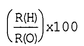
substrat Si/SiO2/(Co eCo/Ni80Fe20 (2,5-2eCo) nm/Co eCo/ Ag 1,1 nm)10.Correlatively, the addition of thin layers of Co to the Permalloy / Ag interfaces increases the amplitude of magnetoresistance of the material. This is illustrated in Figures 3A and 3B. Figure 3A shows a bundle of curves
substrate Si / SiO 2 / (Co e Co / Ni 80 Fe 20 (2,5-2e Co ) nm / Co e Co /
Dans cette expérience, on a gardé l'épaisseur totale des couches magnétiques Co/NiFe/Co constante pour faciliter la comparaison d'un échantillon à l'autre. On constate, sur la figure 3A, une très rapide augmentation de l'amplitude de magnétorésistance lié à l'introduction des couches de Co interfaciales.In this experiment, the total thickness of the Co / NiFe / Co magnetic layers was kept constant to facilitate comparison from one sample to another. There is, in FIG. 3A, a very rapid increase in the amplitude of magnetoresistance linked to the introduction of the layers of interfacial Co.
La figure 3B représente l'amplitude de magnétorésistance en fonction de l'épaisseur eCo des couches de Co. La courbe en trait plein est un ajustement suivant une loi phénoménologique exponentielle :![]()
![]()
Cette courbe montre que l'amplitude de magnétorésistance augmente très vite aux faibles épaisseurs, pour pratiquement saturer lorsqu'une couche monoatomique de Co a été introduite aux interfaces. L'introduction d'un plan atomique de Co aux interfaces Permalloy/Ag suffit donc à doubler l'amplitude de magnétorésistance et à assurer une meilleure stabilité thermique de la structure.This curve shows that the amplitude of magnetoresistance increases very quickly at small thicknesses, to practically saturate when a monoatomic layer of Co has been introduced at the interfaces. The introduction of an atomic plane of Co at the Permalloy / Ag interfaces is therefore sufficient to double the amplitude of magnetoresistance and to ensure better thermal stability of the structure.
Le champ de saturation, malheureusement, augmente également avec l'épaisseur des couches interfaciales de Co. Ceci est nettement visible sur la figure 3A. Le champ de saturation est tracé en fonction de l'épaisseur de Co sur la figure 3C. La courbe en trait plein représente la loi suivante :![]()
![]()
Le champ Hsat augmente un peu moins rapidement que l'amplitude de magnétorésistance en fonction de l'épaisseur de Co. On peut néanmoins réduire ce champ de saturation en jouant sur l'épaisseur d'Ag. Ceci est illustré sur la figure 4A qui représente un faisceau de courbes ![]()
![]()
Les résultats présentés dans le cadre de la présente demande sont surprenants, pour les raisons suivantes.The results presented in the context of the present application are surprising, for the following reasons.
Il est tout d'abord connu dans les multicouches (Co/Ag) dans lesquelles les couches de Co sont très fines (de l'ordre de quelques plans atomiques d'épaisseur), qu'un recuit de ces structures conduit à une coalescence en îlots du Co. Les couches, initialement continues dans l'état brut de dépôt, se disloquent au cours des recuits. Le Co coalesce sous formes d'îlots, qui grossissent et deviennent de plus en plus distants les uns des autres au cours des recuits. Ce processus est décrit par exemple dans la publication de E.A.M. Van Alphen, P.A.A. Van der Heijden, W.L.M. de Jonge, Journal of Magnetism and Magnetic Materials 140-144 (1995) 609. Compte tenu de cet effet, l'homme de l'art ne serait pas enclin à mettre du Co aux interfaces NiFe/Ag car il pourrait craindre qu'une coalescence similaire se produise aux interfaces. Si tel était le cas, on aurait alors une interface discontinue constituée par endroit de NiFe/Ag, à d'autres endroits de NiFe/Co/Ag. Les endroits sans Co constitueraient des points de faiblesse pour la stabilité thermique des multicouches. Or, les résultats expérimentaux obtenus (comparaison des figures 2A, sans Co aux interfaces, et 2B avec Co aux interfaces) montrent que la stabilité thermique est bel et bien augmentée par l'introduction du Co aux interfaces. Ceci implique que la couche de Co introduite à l'interface peut être considérée comme continue, et donc que la coalescence du Co sous forme d'îlots est globalement négligeable ou nulle. Cette différence de comportement des fines couches de Co entre le système (Co/Ag) et celui avec les interfaces NiFe/Co/Ag est certainement due aux différences d'énergie interfaciale des interfaces NiFe/Co et Co/Ag.It is first of all known in multilayers (Co / Ag) in which the Co layers are very thin (of the order of a few atomic planes in thickness), that annealing of these structures leads to coalescence in Islets of Co. The layers, initially continuous in the raw state of deposition, dislocate during annealing. Co coalesces in the form of islets, which grow larger and more more distant from each other during annealing. This process is described for example in the publication of EAM Van Alphen, PAA Van der Heijden, WLM de Jonge, Journal of Magnetism and Magnetic Materials 140-144 (1995) 609. Given this effect, those skilled in the art would not be inclined to put Co at the NiFe / Ag interfaces because he might fear that a similar coalescence would occur at the interfaces. If this were the case, we would then have a discontinuous interface constituted by place of NiFe / Ag, in other places of NiFe / Co / Ag. The places without Co would constitute weak points for the thermal stability of the multilayers. However, the experimental results obtained (comparison of FIGS. 2A, without Co at the interfaces, and 2B with Co at the interfaces) show that the thermal stability is indeed increased by the introduction of Co at the interfaces. This implies that the layer of Co introduced at the interface can be considered as continuous, and therefore that the coalescence of Co in the form of islets is globally negligible or zero. This difference in behavior of the thin layers of Co between the system (Co / Ag) and that with the NiFe / Co / Ag interfaces is certainly due to the differences in interfacial energy of the NiFe / Co and Co / Ag interfaces.
Un autre problème qui aurait pu survenir au cours des recuits sur des multicouches Permalloy/Ag, avec Co aux interfaces, provient de la miscibilité du Permalloy et du Co. Les recuits effectués auraient pu conduire à une diffusion du Co à l'intérieur du Permalloy. Les interfaces se seraient alors progressivement appauvries en Co, ce qui aurait conduit à observer dans les multicouches Co/NiFe/Co/Ag les mêmes caractéristiques de stabilité thermique que dans des multicouches NiFe/Ag. Ce phénomène ne se produit pas ou très peu car, comme le montrent les figures 2A et 2B, la stabilité thermique du composé multicouche est augmentée e par l'ajout de Co aux interfaces. Une certaine diffusion du Co dans le Permalloy doit effectivement se produire, mais doit rester suffisamment limitée pour ne pas complètement perdre le bénéfice sur la stabilité thermique.Another problem that could have arisen during annealing on Permalloy / Ag multilayers, with Co at the interfaces, arises from the miscibility of Permalloy and Co. The annealing carried out could have led to diffusion of Co inside the Permalloy . The interfaces would then be progressively depleted in Co, which would have led to observe in the Co / NiFe / Co / Ag multilayers the same characteristics of thermal stability as in NiFe / Ag multilayers. This phenomenon only occurs not or very little because, as shown in FIGS. 2A and 2B, the thermal stability of the multilayer compound is increased by the addition of Co at the interfaces. A certain diffusion of Co in the Permalloy must indeed occur, but must remain sufficiently limited so as not to completely lose the benefit on the thermal stability.
Les structures données en exemple dans le présent document ont été préparées par pulvérisation cathodique. Le vide de base dans l'enceinte d'élaboration était de l'ordre de 2.10-8 mbar. L'argon, à une pression de 1.5.10-3 mbar, était utilisé comme gaz pour la pulvérisation. La cible de NiFe était alimentée par une source RF, les cibles de Co et d'Ag par des sources DC. Les substrats étaient refroidis, pendant les dépôts de ces matériaux, à une température proche de celle de l'azote liquide, pour éviter la coalescence des couches d'Ag. D'autres techniques d'élaboration des couches minces métalliques pourraient être utilisées pour la préparation de ces matériaux, telles que l'épitaxie par jet moléculaire ou la pulvérisation par faisceau d'ions.The structures given as examples in this document were prepared by sputtering. The basic vacuum in the production enclosure was of the order of 2.10 -8 mbar. Argon, at a pressure of 1.5.10 -3 mbar, was used as the gas for spraying. The NiFe target was powered by an RF source, the Co and Ag targets by DC sources. The substrates were cooled, during the deposition of these materials, to a temperature close to that of liquid nitrogen, to avoid the coalescence of the layers of Ag. Other techniques for developing thin metallic layers could be used for the preparation of these materials, such as molecular beam epitaxy or ion beam sputtering.
Une structure magnétique selon l'invention peut être utilisée pour réaliser un capteur de courant tel que décrit dans la demande FR-2 710 753 (DD 1289).A magnetic structure according to the invention can be used to produce a current sensor as described in application FR-2 710 753 (DD 1289).
La figure 5 représente un tel capteur de courant 20, en position de mesure d'un courant I parcourant un conducteur électrique 22. Le capteur de courant 20 en forme d'anneau comporte un ruban magnétorésistif 24 également en forme d'anneau. Les extrémités 26 et 28 du ruban 24 sont disposées à proximité l'une de l'autre de façon que le ruban forme un cercle presque complet. Ces extrémités sont aménagées pour permettre la connexion électrique du ruban 24 avec un générateur de courant continu i (ou de tension). L'observation de la tension v aux bornes du ruban 24 permet de constater la variation de la résistance du ruban sous l'effet du champ magnétique HI induit par le courant I.FIG. 5 represents such a
Ce même document décrit également un circuit électrique pour la mesure de I. Il décrit aussi un procédé de réalisation dudit capteur.This same document also describes an electrical circuit for the measurement of I. It also describes a method for producing said sensor.
Une structure magnétique selon l'invention peut également être utilisée pour réaliser une tête magnétique.A magnetic structure according to the invention can also be used to produce a magnetic head.
La figure 6 montre, à titre illustratif, comment mettre en oeuvre l'invention dans une tête magnétique d'écriture et/ou de lecture. Une telle tête a été décrite dans la demande de brevet français n°93 13249 déposée le 8 novembre 1993.FIG. 6 shows, by way of illustration, how to implement the invention in a magnetic writing and / or reading head. Such a head has been described in French patent application No. 93 13249 filed on November 8, 1993.
La tête est représentée en coupe. On y voit un substrat 30, une couche magnétique inférieure 32, deux piliers magnétiques 341, 342, un bobinage conducteur 36, deux pièces magnétiques 401, 402 formant un premier entrefer 42, un élément magnétorésistant multicouche 50 placé au-dessus de l'entrefer 42, un conducteur de polarisation 80, traversé par un courant circulant perpendiculairement au plan de la figure, deux pièces polaires 901, 902 définissant un second entrefer 100, qui est l'entrefer défilant devant le support d'enregistrement magnétique (non représenté), le tout étant noyé dans un isolant 102.The head is shown in section. We see a
Par réglage du courant circulant dans le conducteur 80, on polarisera la magnétorésistance 50 à une valeur appropriée.By adjusting the current flowing in the
D'une façon générale, le principal avantage apporté par l'invention est d'augmenter la stabilité des propriétés structurales du matériau au cours de recuit à des températures allant au moins de 250°C à 300°C, températures auxquelles le matériau peut être soumis lors des procédés lithographiques. Par ailleurs, l'adjonction de fines couches interfaciales de Co, ou d'alliages riches en Co, aux interfaces Permalloy/Ag permet d'augmenter l'amplitude de magnétorésistance ce qui, notamment dans les structures vanne de spin, conduit à une augmentation de la sensibilité du matériau (augmentation de ΔR/R sans augmentation significative de la variation de champ nécessaire à observer toute l'amplitude de magnétorésistance).In general, the main advantage provided by the invention is to increase the stability of the structural properties of the material during annealing at temperatures ranging from at least 250 ° C to 300 ° C, temperatures to which the material can be subjected during lithographic processes. Furthermore, the addition of thin interfacial layers of Co, or of alloys rich in Co, to the Permalloy / Ag interfaces makes it possible to increase the amplitude of magnetoresistance which, in particular in spin valve structures, leads to an increase the sensitivity of the material (increase in ΔR / R without significant increase in the field variation necessary to observe the entire amplitude of magnetoresistance).
Claims (19)
Ni100-x-y-zCoxFeyAz où 0≤x<100, 0≤y≤100 et o≤z≤40, et 0≤x+y+z≤100Magnetic structure according to claim 1, the magnetic material being of formula:
Ni 100-xyz Co x Fe y A z where 0≤x <100, 0≤y≤100 and o≤z≤40, and 0≤x + y + z≤100
Applications Claiming Priority (2)
| Application Number | Priority Date | Filing Date | Title |
|---|---|---|---|
| FR9514898 | 1995-12-15 | ||
| FR9514898A FR2742571B1 (en) | 1995-12-15 | 1995-12-15 | MULTI-LAYERED STRUCTURE AND SENSOR AND METHOD FOR PRODUCING THE SAME |
Publications (2)
| Publication Number | Publication Date |
|---|---|
| EP0779632A1 true EP0779632A1 (en) | 1997-06-18 |
| EP0779632B1 EP0779632B1 (en) | 2002-09-11 |
Family
ID=9485551
Family Applications (1)
| Application Number | Title | Priority Date | Filing Date |
|---|---|---|---|
| EP96402718A Expired - Lifetime EP0779632B1 (en) | 1995-12-15 | 1996-12-12 | Multilayer structure and sensor and fabrication process |
Country Status (5)
| Country | Link |
|---|---|
| US (1) | US6013365A (en) |
| EP (1) | EP0779632B1 (en) |
| JP (1) | JPH09199325A (en) |
| DE (1) | DE69623577T2 (en) |
| FR (1) | FR2742571B1 (en) |
Cited By (5)
| Publication number | Priority date | Publication date | Assignee | Title |
|---|---|---|---|---|
| US9804234B2 (en) | 2014-01-09 | 2017-10-31 | Allegro Microsystems, Llc | Magnetoresistance element with an improved seed layer to promote an improved response to magnetic fields |
| US9812637B2 (en) | 2015-06-05 | 2017-11-07 | Allegro Microsystems, Llc | Spin valve magnetoresistance element with improved response to magnetic fields |
| US10620279B2 (en) | 2017-05-19 | 2020-04-14 | Allegro Microsystems, Llc | Magnetoresistance element with increased operational range |
| US11022661B2 (en) | 2017-05-19 | 2021-06-01 | Allegro Microsystems, Llc | Magnetoresistance element with increased operational range |
| US11719771B1 (en) | 2022-06-02 | 2023-08-08 | Allegro Microsystems, Llc | Magnetoresistive sensor having seed layer hysteresis suppression |
Families Citing this family (26)
| Publication number | Priority date | Publication date | Assignee | Title |
|---|---|---|---|---|
| JP3456204B2 (en) * | 2001-01-09 | 2003-10-14 | 日立金属株式会社 | Magnetic encoder |
| US8382821B2 (en) * | 1998-12-03 | 2013-02-26 | Medinol Ltd. | Helical hybrid stent |
| US6821652B1 (en) | 1999-06-08 | 2004-11-23 | Fujitsu Limited | Magnetic recording medium and magnetic storage apparatus |
| US6753101B1 (en) | 1999-06-08 | 2004-06-22 | Fujitsu Limited | Magnetic recording medium, magnetic storage apparatus, recording method and method of producing magnetic recording medium |
| US6602612B2 (en) | 1999-06-08 | 2003-08-05 | Fujitsu Limited | Magnetic recording medium and magnetic storage apparatus |
| US6645646B1 (en) | 1999-06-08 | 2003-11-11 | Fujitsu Limited | Magnetic recording medium and magnetic storage apparatus |
| US6689495B1 (en) | 1999-06-08 | 2004-02-10 | Fujitsu Limited | Magnetic recording medium and magnetic storage apparatus |
| US6280813B1 (en) * | 1999-10-08 | 2001-08-28 | International Business Machines Corporation | Magnetic recording media with antiferromagnetically coupled ferromagnetic films as the recording layer |
| JP2001284123A (en) * | 2000-01-24 | 2001-10-12 | Fuji Electric Co Ltd | Magnetic thin film, magnetic component provided with the same, their manufacturing method, and electric power converter |
| US6835576B2 (en) * | 2000-05-02 | 2004-12-28 | Fuji Electric Co., Ltd. | Magnetic thin film, a magnetic component that uses this magnetic thin film, manufacturing methods for the same, and a power conversion device |
| US6645614B1 (en) | 2000-07-25 | 2003-11-11 | Seagate Technology Llc | Magnetic recording media having enhanced coupling between magnetic layers |
| JP4382333B2 (en) * | 2002-03-28 | 2009-12-09 | 株式会社東芝 | Magnetoresistive element, magnetic head, and magnetic reproducing apparatus |
| JP2005025890A (en) * | 2003-07-04 | 2005-01-27 | Fujitsu Ltd | Magnetic film for magnetic head |
| JP4786331B2 (en) | 2005-12-21 | 2011-10-05 | 株式会社東芝 | Method for manufacturing magnetoresistive element |
| JP4514721B2 (en) * | 2006-02-09 | 2010-07-28 | 株式会社東芝 | Magnetoresistive element manufacturing method, magnetoresistive element, magnetoresistive head, magnetic recording / reproducing apparatus, and magnetic storage apparatus |
| JP2007299880A (en) * | 2006-04-28 | 2007-11-15 | Toshiba Corp | Magnetoresistance effect element and its manufacturing method |
| JP4550777B2 (en) | 2006-07-07 | 2010-09-22 | 株式会社東芝 | Magnetoresistive element manufacturing method, magnetoresistive element, magnetic head, magnetic recording / reproducing apparatus, and magnetic memory |
| JP5044157B2 (en) * | 2006-07-11 | 2012-10-10 | 株式会社東芝 | Magnetoresistive element, magnetic head, and magnetic reproducing apparatus |
| JP2008085202A (en) | 2006-09-28 | 2008-04-10 | Toshiba Corp | Magnetoresistance effect element, magnetic memory, magnetic head, and magnetic recording and reproducing device |
| JP4388093B2 (en) | 2007-03-27 | 2009-12-24 | 株式会社東芝 | Magnetoresistive element, magnetic head, magnetic recording / reproducing apparatus |
| JP5150284B2 (en) | 2008-01-30 | 2013-02-20 | 株式会社東芝 | Magnetoresistive element and manufacturing method thereof |
| JP5361201B2 (en) * | 2008-01-30 | 2013-12-04 | 株式会社東芝 | Method for manufacturing magnetoresistive element |
| JP5039006B2 (en) | 2008-09-26 | 2012-10-03 | 株式会社東芝 | Magnetoresistive element manufacturing method, magnetoresistive element, magnetic head assembly, and magnetic recording / reproducing apparatus |
| JP5039007B2 (en) | 2008-09-26 | 2012-10-03 | 株式会社東芝 | Magnetoresistive element manufacturing method, magnetoresistive element, magnetic head assembly, and magnetic recording / reproducing apparatus |
| JP2010080839A (en) | 2008-09-29 | 2010-04-08 | Toshiba Corp | Method of manufacturing magneto-resistance effect device, the magneto-resistance effect device, magnetic head assembly, and magnetic recording and reproducing apparatus |
| WO2012172730A2 (en) * | 2011-06-14 | 2012-12-20 | Panasonic Corporation | Solar cell and method for fabricating the same |
Citations (1)
| Publication number | Priority date | Publication date | Assignee | Title |
|---|---|---|---|---|
| JPH0567525A (en) * | 1991-09-06 | 1993-03-19 | Tdk Corp | Magnetic laminated body, its manufacture, and manufacture of magneto-resistance effect element |
Family Cites Families (4)
| Publication number | Priority date | Publication date | Assignee | Title |
|---|---|---|---|---|
| US5549978A (en) * | 1992-10-30 | 1996-08-27 | Kabushiki Kaisha Toshiba | Magnetoresistance effect element |
| FR2698965B1 (en) * | 1992-12-03 | 1995-01-06 | Commissariat Energie Atomique | Structure and magnetic sensor multilayer with strong magnetoresistance and method of manufacturing the structure. |
| FR2710753B1 (en) * | 1993-09-27 | 1995-10-27 | Commissariat Energie Atomique | Current sensor comprising a magnetoresistive tape and its production method. |
| FR2712420B1 (en) * | 1993-11-08 | 1995-12-15 | Commissariat Energie Atomique | Magnetic read head with multilayer magnetoresistive element and concentrator and method of making the same. |
-
1995
- 1995-12-15 FR FR9514898A patent/FR2742571B1/en not_active Expired - Fee Related
-
1996
- 1996-12-05 US US08/760,798 patent/US6013365A/en not_active Expired - Fee Related
- 1996-12-10 JP JP8330036A patent/JPH09199325A/en active Pending
- 1996-12-12 EP EP96402718A patent/EP0779632B1/en not_active Expired - Lifetime
- 1996-12-12 DE DE69623577T patent/DE69623577T2/en not_active Expired - Fee Related
Patent Citations (1)
| Publication number | Priority date | Publication date | Assignee | Title |
|---|---|---|---|---|
| JPH0567525A (en) * | 1991-09-06 | 1993-03-19 | Tdk Corp | Magnetic laminated body, its manufacture, and manufacture of magneto-resistance effect element |
Non-Patent Citations (4)
| Title |
|---|
| ALPHEN VAN E A M ET AL: "INFLUENCE OF ANNEALING ON THE STRUCTURAL AND MAGNETIC PROPERTIES OF CO/AG MULTILAYERS WITH THIN CO LAYERS", JOURNAL OF MAGNETISM AND MAGNETIC MATERIALS, vol. 140/144, no. PART 01, 1 February 1995 (1995-02-01), pages 609/610, XP000490423 * |
| ETIENNE P ET AL: "MOLECULAR BEAM EPITAXIAL GROWTH OF CR/FE,AG/FE,AG/CR AND AG/CO SUPERLATTICES ON MGO (001) SUBSTRATES", JOURNAL OF CRYSTAL GROWTH, vol. 111, no. 1 / 04, 2 May 1991 (1991-05-02), pages 1003 - 1010, XP000298483 * |
| PATENT ABSTRACTS OF JAPAN vol. 017, no. 383 (E - 1400) 19 July 1993 (1993-07-19) * |
| STEREN L B ET AL: "GIANT MAGNETORESISTANCE IN HYBRID MAGNETIC NANOSTRUCTURES", JOURNAL OF MAGNETISM AND MAGNETIC MATERIALS, vol. 140/144, no. PART 01, 1 February 1995 (1995-02-01), pages 495/496, XP000490388 * |
Cited By (8)
| Publication number | Priority date | Publication date | Assignee | Title |
|---|---|---|---|---|
| US9804234B2 (en) | 2014-01-09 | 2017-10-31 | Allegro Microsystems, Llc | Magnetoresistance element with an improved seed layer to promote an improved response to magnetic fields |
| US9922673B2 (en) | 2014-01-09 | 2018-03-20 | Allegro Microsystems, Llc | Magnetoresistance element with improved response to magnetic fields |
| US10347277B2 (en) | 2014-01-09 | 2019-07-09 | Allegro Microsystems, Llc | Magnetoresistance element with improved response to magnetic fields |
| US9812637B2 (en) | 2015-06-05 | 2017-11-07 | Allegro Microsystems, Llc | Spin valve magnetoresistance element with improved response to magnetic fields |
| US10620279B2 (en) | 2017-05-19 | 2020-04-14 | Allegro Microsystems, Llc | Magnetoresistance element with increased operational range |
| US11002807B2 (en) | 2017-05-19 | 2021-05-11 | Allegro Microsystems, Llc | Magnetoresistance element with increased operational range |
| US11022661B2 (en) | 2017-05-19 | 2021-06-01 | Allegro Microsystems, Llc | Magnetoresistance element with increased operational range |
| US11719771B1 (en) | 2022-06-02 | 2023-08-08 | Allegro Microsystems, Llc | Magnetoresistive sensor having seed layer hysteresis suppression |
Also Published As
| Publication number | Publication date |
|---|---|
| FR2742571A1 (en) | 1997-06-20 |
| EP0779632B1 (en) | 2002-09-11 |
| DE69623577T2 (en) | 2003-05-22 |
| US6013365A (en) | 2000-01-11 |
| JPH09199325A (en) | 1997-07-31 |
| DE69623577D1 (en) | 2002-10-17 |
| FR2742571B1 (en) | 1998-01-16 |
Similar Documents
| Publication | Publication Date | Title |
|---|---|---|
| EP0779632B1 (en) | Multilayer structure and sensor and fabrication process | |
| EP1055259B1 (en) | Magnetoresistor with tunnel effect and magnetic sensor using same | |
| EP0724302B1 (en) | Magnetic sensor with a giant magnetoresistance, and its method of fabrication | |
| EP2106612B1 (en) | Multilayer magnetic device, process for the production thereof, magnetic field sensor, magnetic memory and logic gate using such a device | |
| EP2286473B1 (en) | Three-layer magnetic element, method for the production thereof, magnetic field sensor, magnetic memory, and magnetic logic gate using such an element | |
| EP1435101B1 (en) | Spin-valve magnetoresistive device with enhanced performance | |
| US7417832B1 (en) | Magnetoresistive structure having a novel specular and filter layer combination | |
| US7684160B1 (en) | Magnetoresistive structure having a novel specular and barrier layer combination | |
| US6574079B2 (en) | Magnetic tunnel junction device and method including a tunneling barrier layer formed by oxidations of metallic alloys | |
| US7564661B2 (en) | Magnetic sensing element including free layer having gradient composition and method for manufacturing the same | |
| FR2743930A1 (en) | MAGNETIC SENSOR FOR READING RECORDING MEDIA | |
| EP0652550A1 (en) | Read-out magnetic head with multilayer magnetoresistant element and concentrator and manufacturing method | |
| EP0721670B1 (en) | Current sensor comprising a magnetoresistive strip and method of production | |
| US7738218B2 (en) | Magnetic detection head and method for manufacturing the same | |
| FR2771511A1 (en) | Magnetic field sensor having ferromagnetic particle layer within nonmagnetic insulating layer | |
| EP0642030B1 (en) | Tongued magnetic flux guide and magnetic sensor, equipped with such a guide | |
| EP1195821A1 (en) | Spin valve device with spin-dependent specular reflection | |
| EP0642181A1 (en) | Magnetoresistive device and sensor with a geometric repetitive pattern | |
| US20080144231A1 (en) | Magnetoresistive head, magnetic storage apparatus and method of manufacturing a magnetic head | |
| FR2701167A1 (en) | Component having a magnetoresistive effect | |
| WO2004051629A1 (en) | Magnetic disk apparatus and method for manufacturing same | |
| JP2006196745A (en) | Magnetic detector and its manufacturing method | |
| JPH05143936A (en) | Magneto-resistance effect type head |
Legal Events
| Date | Code | Title | Description |
|---|---|---|---|
| PUAI | Public reference made under article 153(3) epc to a published international application that has entered the european phase |
Free format text: ORIGINAL CODE: 0009012 |
|
| AK | Designated contracting states |
Kind code of ref document: A1 Designated state(s): CH DE GB LI NL |
|
| 17P | Request for examination filed |
Effective date: 19971121 |
|
| 17Q | First examination report despatched |
Effective date: 19990721 |
|
| GRAG | Despatch of communication of intention to grant |
Free format text: ORIGINAL CODE: EPIDOS AGRA |
|
| GRAG | Despatch of communication of intention to grant |
Free format text: ORIGINAL CODE: EPIDOS AGRA |
|
| GRAH | Despatch of communication of intention to grant a patent |
Free format text: ORIGINAL CODE: EPIDOS IGRA |
|
| GRAH | Despatch of communication of intention to grant a patent |
Free format text: ORIGINAL CODE: EPIDOS IGRA |
|
| GRAA | (expected) grant |
Free format text: ORIGINAL CODE: 0009210 |
|
| AK | Designated contracting states |
Kind code of ref document: B1 Designated state(s): CH DE GB LI NL |
|
| REG | Reference to a national code |
Ref country code: GB Ref legal event code: FG4D Free format text: NOT ENGLISH |
|
| REG | Reference to a national code |
Ref country code: CH Ref legal event code: EP |
|
| REF | Corresponds to: |
Ref document number: 69623577 Country of ref document: DE Date of ref document: 20021017 |
|
| GBT | Gb: translation of ep patent filed (gb section 77(6)(a)/1977) |
Effective date: 20021125 |
|
| PLBE | No opposition filed within time limit |
Free format text: ORIGINAL CODE: 0009261 |
|
| STAA | Information on the status of an ep patent application or granted ep patent |
Free format text: STATUS: NO OPPOSITION FILED WITHIN TIME LIMIT |
|
| 26N | No opposition filed |
Effective date: 20030612 |
|
| PGFP | Annual fee paid to national office [announced via postgrant information from national office to epo] |
Ref country code: NL Payment date: 20061203 Year of fee payment: 11 |
|
| PGFP | Annual fee paid to national office [announced via postgrant information from national office to epo] |
Ref country code: GB Payment date: 20061206 Year of fee payment: 11 |
|
| PGFP | Annual fee paid to national office [announced via postgrant information from national office to epo] |
Ref country code: CH Payment date: 20061221 Year of fee payment: 11 |
|
| PGFP | Annual fee paid to national office [announced via postgrant information from national office to epo] |
Ref country code: DE Payment date: 20061223 Year of fee payment: 11 |
|
| REG | Reference to a national code |
Ref country code: CH Ref legal event code: PL |
|
| GBPC | Gb: european patent ceased through non-payment of renewal fee |
Effective date: 20071212 |
|
| NLV4 | Nl: lapsed or anulled due to non-payment of the annual fee |
Effective date: 20080701 |
|
| PG25 | Lapsed in a contracting state [announced via postgrant information from national office to epo] |
Ref country code: LI Free format text: LAPSE BECAUSE OF NON-PAYMENT OF DUE FEES Effective date: 20071231 Ref country code: DE Free format text: LAPSE BECAUSE OF NON-PAYMENT OF DUE FEES Effective date: 20080701 Ref country code: CH Free format text: LAPSE BECAUSE OF NON-PAYMENT OF DUE FEES Effective date: 20071231 |
|
| PG25 | Lapsed in a contracting state [announced via postgrant information from national office to epo] |
Ref country code: NL Free format text: LAPSE BECAUSE OF NON-PAYMENT OF DUE FEES Effective date: 20080701 |
|
| PG25 | Lapsed in a contracting state [announced via postgrant information from national office to epo] |
Ref country code: GB Free format text: LAPSE BECAUSE OF NON-PAYMENT OF DUE FEES Effective date: 20071212 |