EP0772839B1 - Versorgungsspannungsaufbereitungsschaltung sowie datenträger mit einer versorgungsspannungsaufbereitungsschaltung - Google Patents
Versorgungsspannungsaufbereitungsschaltung sowie datenträger mit einer versorgungsspannungsaufbereitungsschaltung Download PDFInfo
- Publication number
- EP0772839B1 EP0772839B1 EP96913695A EP96913695A EP0772839B1 EP 0772839 B1 EP0772839 B1 EP 0772839B1 EP 96913695 A EP96913695 A EP 96913695A EP 96913695 A EP96913695 A EP 96913695A EP 0772839 B1 EP0772839 B1 EP 0772839B1
- Authority
- EP
- European Patent Office
- Prior art keywords
- supply voltage
- processing circuit
- voltage processing
- parallel
- data carrier
- Prior art date
- Legal status (The legal status is an assumption and is not a legal conclusion. Google has not performed a legal analysis and makes no representation as to the accuracy of the status listed.)
- Expired - Lifetime
Links
Images
Classifications
-
- G—PHYSICS
- G06—COMPUTING OR CALCULATING; COUNTING
- G06K—GRAPHICAL DATA READING; PRESENTATION OF DATA; RECORD CARRIERS; HANDLING RECORD CARRIERS
- G06K19/00—Record carriers for use with machines and with at least a part designed to carry digital markings
- G06K19/06—Record carriers for use with machines and with at least a part designed to carry digital markings characterised by the kind of the digital marking, e.g. shape, nature, code
- G06K19/067—Record carriers with conductive marks, printed circuits or semiconductor circuit elements, e.g. credit or identity cards also with resonating or responding marks without active components
- G06K19/07—Record carriers with conductive marks, printed circuits or semiconductor circuit elements, e.g. credit or identity cards also with resonating or responding marks without active components with integrated circuit chips
- G06K19/0723—Record carriers with conductive marks, printed circuits or semiconductor circuit elements, e.g. credit or identity cards also with resonating or responding marks without active components with integrated circuit chips the record carrier comprising an arrangement for non-contact communication, e.g. wireless communication circuits on transponder cards, non-contact smart cards or RFIDs
Definitions
- the present invention relates to a Supply voltage processing circuit, especially for contactless, passive, inductive data carriers that include a rectifier, a backup capacitor and a parallel to the Support capacitor switched direct parallel regulator stage; it also affects one contactless, passive, inductive data carrier with one antenna and one Supply voltage conditioning circuit.
- Data transmission systems for data transmission between one normally stationary read / write station and several data carriers are known.
- the disks serve as intelligent, mobile data storage in the near field of read / write stations be put into operation for writing or reading out data.
- Such systems are in various forms with regard to transmission range, Data transfer speed, degree of integration, storage capacity and intelligence of the Data carriers etc. and in various applications such as access control, industrial and commercial property identification, immobilizers, automatic trip control, etc. used.
- Another example is the automatic toll collection as soon as one comes on a data carrier attached to a vehicle at a read / write station of a toll station passes by.
- a conventional power supply is used for the data carrier Supply voltage conditioning circuit that includes a rectifier, a backup capacitor and a direct parallel regulator stage connected in parallel to the backup capacitor (e.g. in the form a Zener diode)
- the problem arises that relatively long interruptions of the HF signal are necessary so that they can be reliably recognized by the data carrier.
- this is because Interruption of the RF signal, the power supply of the data carrier exclusively takes place from the support capacitor and therefore the antenna coil is in no way loaded, so that this resonates for a longer time due to resonance phenomena.
- Another disadvantage is that the parallel controller stage must absorb relatively high currents when the Data carrier is passed very close to the read / write station. For this reason its control speed inevitably relatively low, so that the voltage control is not is satisfactory.
- a Supply voltage conditioning circuit can be created, the more stabilized Supply voltage supplies. Also, the reliability of the disk, in particular their strength with respect to static charges can be increased.
- the direct Parallel controller stage decoupled - e.g. another indirect one directly at the rectifier Parallel controller stage is provided.
- This indirect parallel controller stage is used for rough control; it can absorb high currents, but is therefore relatively slow, i.e. your Control speed is slow. So since a rough regulation is already from the indirect one Regulator stage is carried out, the direct regulator stage requires only relatively low currents record so that it can have a correspondingly higher control speed; this makes the regulation of the supply voltage very good.
- Another advantage of Indirect regulator stage is that it is also during the interruptions of the RF signal loads the antenna coil, so that their vibrations are strongly damped and thus very short interruptions can be reliably detected.
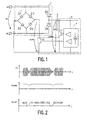
- FIG. 1 the basic circuit diagram of a data carrier according to the invention
- Fig. 2 the time course of voltages at certain points within the circuit of the data carrier Fig. 1.
- FIG. 1 shows the basic circuit of the supply voltage processing circuit.
- a coil is connected to the connections LA and LB.
- the RF signal received by this is fed to the supply voltage processing circuit.
- This consists of a rectifier network 1 (diodes D1-D6), preferably implemented with MOS transistors, which generates two decoupled rectified voltages U LAST and U VERS from the applied AC voltage U L , from a supporting capacitance 2 for smoothing the actual supply voltage U VERS and a voltage regulator circuit 3.
- the voltage regulator circuit 3 consists of two parallel regulators, each with a transistor driver T1 or T2 and a control amplifier stage with reference voltage 4.
- Both regulator stages operate according to the parallel regulator principle, ie the driver transistors are activated as soon as the supply voltage U VERS reaches a permissible value, which is derived from the reference voltage. By activating the driver transistors, current is drawn from the supply circuit and the supply voltage is thus dampened to a permissible value.
- the first regulator circuit with driver stage T1 has a fast regulation characteristic and is therefore able to compensate for changes in the AC voltage very quickly. In cooperation with the supporting capacitance 2, this results in a very constant supply voltage U VERS even with rapid amplitude changes in the antenna alternating voltage U L (see FIG. 2).
- the driver transistor T1 must be small and therefore weakly dimensioned and is therefore unable to derive large currents with very strong energy coupling.
- the second control stage with driver transistor T2 fulfills this task. Due to the size and high driver strength of transistor T2, the behavior of the second controller is rather sluggish. T2 does not act directly on the supply voltage U VERS , but only dampens it indirectly by damping the AC voltage amplitude via its own diode network for the load voltage U LAST . Due to the inertia of the second regulator, the load voltage U LAST is subject to very strong fluctuations and usually collapses completely during the energy pauses (see FIG. 2), and in addition the antenna AC voltage U L is strongly damped during the energy pauses, which leads to a rapid decay of U. L leads in the energy pauses (see also FIG.
- the supply voltage processing circuit described unites itself essential features, especially for contactless data carrier systems of large Benefits are, like high ESD protection, high data transfer rate for Pause distance modulation and complete, space-efficient, monolithic integration.
Landscapes
- Engineering & Computer Science (AREA)
- Computer Networks & Wireless Communication (AREA)
- Computer Hardware Design (AREA)
- Microelectronics & Electronic Packaging (AREA)
- Physics & Mathematics (AREA)
- General Physics & Mathematics (AREA)
- Theoretical Computer Science (AREA)
- Near-Field Transmission Systems (AREA)
- Transmitters (AREA)
Description
Claims (2)
- Versorgungsspannungsaufbereitungsschaltung, insbesondere für kontaktlose, passive, induktive Datenträger, die ein Gleichrichternetzwerk (1), einen Stützkondensator (2) und eine parallel zum Stützkondensator (2) geschaltete erste Parallelreglerstufe (T1) aufweist,
dadurch gekennzeichnet, daß das Gleichrichternetzwerk (1) zum Erzeugen zweier voneinander entkoppelter gleichgerichteter Spannungen (ULAST, UVERS) ausgebildet ist, von denen eine (UVERS) dem Stützkondensator (2) und der dazu parallel geschalteten ersten Parallelreglerstufe (T1) zugeführt wird, und daß zusätzlich direkt am Gleichrichternetzwerk (1) eine zweite Parallelreglerstufe (T2) vorgesehen ist, die von der ersten Parallelreglerstufe (T1) entkoppelt (D3, D4; D5, D6) ist, der die zweite (ULAST) der voneinander entkoppelten gleichgerichteten Spannungen (ULAST , UVERS) zugeführt wird und die eine höhere Strombelastbarkeit und dadurch ein langsameres Regelverhalten aufweist als die erste Parallelreglerstufe (T1). - Kontaktloser, passiver, induktiver Datenträger mit einer Antenne und einer Versorgungsspannungsaufbereitungsschaltung,
dadurch gekennzeichnet, daß die Versorgungsspannungsaufbereitungsschaltung nach Anspruch 1 ausgebildet ist und daß keine zusätzliche Überspannungsschutzschaltung an den Antennenanschlüssen (LA, LB) vorgesehen ist.
Priority Applications (1)
| Application Number | Priority Date | Filing Date | Title |
|---|---|---|---|
| AT96913695T ATE239949T1 (de) | 1995-05-31 | 1996-05-30 | Versorgungsspannungsaufbereitungsschaltung sowie datenträger mit einer versorgungsspannungsaufbereitungsschaltung |
Applications Claiming Priority (4)
| Application Number | Priority Date | Filing Date | Title |
|---|---|---|---|
| AT0091895A ATA91895A (de) | 1995-05-31 | 1995-05-31 | Versorgungsspannungsaufbereitungsschaltung sowie datenträger mit einer versorgungsspannungsaufbereitungsschaltung |
| AT918955 | 1995-05-31 | ||
| AT9189/55 | 1995-05-31 | ||
| PCT/IB1996/000517 WO1996038805A2 (de) | 1995-05-31 | 1996-05-30 | Versorgungsspannungsaufbereitungsschaltung sowie datenträger mit einer versorgungsspannungsaufbereitungsschaltung |
Publications (2)
| Publication Number | Publication Date |
|---|---|
| EP0772839A2 EP0772839A2 (de) | 1997-05-14 |
| EP0772839B1 true EP0772839B1 (de) | 2003-05-07 |
Family
ID=3502827
Family Applications (1)
| Application Number | Title | Priority Date | Filing Date |
|---|---|---|---|
| EP96913695A Expired - Lifetime EP0772839B1 (de) | 1995-05-31 | 1996-05-30 | Versorgungsspannungsaufbereitungsschaltung sowie datenträger mit einer versorgungsspannungsaufbereitungsschaltung |
Country Status (7)
| Country | Link |
|---|---|
| US (1) | US5874829A (de) |
| EP (1) | EP0772839B1 (de) |
| JP (1) | JP3938404B2 (de) |
| CN (1) | CN1133950C (de) |
| AT (1) | ATA91895A (de) |
| DE (1) | DE59610420D1 (de) |
| WO (1) | WO1996038805A2 (de) |
Families Citing this family (17)
| Publication number | Priority date | Publication date | Assignee | Title |
|---|---|---|---|---|
| JPH10135882A (ja) * | 1996-10-24 | 1998-05-22 | Toshiba Corp | 非接触式情報記録媒体及びそのデータ送信方式 |
| US6091935A (en) * | 1997-10-07 | 2000-07-18 | Microchip Technology Incorporated | Integrated circuit transporter and a method of communication therefor |
| FR2776865B1 (fr) * | 1998-03-31 | 2000-05-05 | Commissariat Energie Atomique | Dispositif de teletransmission par couplage inductif |
| EP0993652B1 (de) * | 1998-05-05 | 2006-10-11 | Koninklijke Philips Electronics N.V. | Datenträger mit korrekturmöglichkeiten und verbesserter spannungsbegrenzungsmöglichkeit |
| FR2781074B1 (fr) | 1998-07-08 | 2006-04-28 | Commissariat Energie Atomique | Interface analogique pour circuit d'echange d'informations autonome |
| FR2811790A1 (fr) * | 2000-07-11 | 2002-01-18 | Schlumberger Systems & Service | Microcontroleur securise contre des attaques dites en courant |
| WO2003065302A1 (en) * | 2002-02-01 | 2003-08-07 | Koninklijke Philips Electronics N.V. | Adapting coil voltage of a tag to field strength |
| CN100397416C (zh) * | 2002-05-27 | 2008-06-25 | Nxp股份有限公司 | 具有用于评估自同步信号信息的信号评估装置的无源数据载体 |
| US6954053B2 (en) * | 2002-07-10 | 2005-10-11 | Atmel Corporation | Interface for shunt voltage regulator in a contactless smartcard |
| US20080055086A1 (en) * | 2004-09-14 | 2008-03-06 | Koninklijke Philips Electronics, N.V. | Overvoltage Protection Device and Radio Frequency Receiver and Radio Frequency Identification Tag Comprising such a Device |
| WO2006040726A1 (en) * | 2004-10-15 | 2006-04-20 | Koninklijke Philips Electronics N.V. | Method of operating a rfid system |
| EP1672563B1 (de) | 2004-12-16 | 2007-10-10 | EM Microelectronic-Marin SA | Radiofrequenz-Transponder, insbesondere für UHF, mit einer ESD-Schutzschaltung |
| JP2009519699A (ja) | 2005-12-15 | 2009-05-14 | エヌエックスピー ビー ヴィ | 無線周波数識別タグ用無線周波数インターフェース回路 |
| EP2047349A1 (de) * | 2006-07-28 | 2009-04-15 | Osram Gesellschaft mit Beschränkter Haftung | Spannungsverorgungsschaltung und verfahren |
| US7889528B2 (en) * | 2006-11-29 | 2011-02-15 | Semiconductor Energy Laroratory Co., Ltd. | Rectifier circuit, power supply circuit, and semiconductor device |
| EP2963587B1 (de) | 2014-07-04 | 2017-03-15 | Nxp B.V. | Spannungswandler |
| US12380309B2 (en) | 2023-11-17 | 2025-08-05 | Nxp B.V. | Radio frequency voltage limiter for an RFID transponder |
Family Cites Families (4)
| Publication number | Priority date | Publication date | Assignee | Title |
|---|---|---|---|---|
| ZA89871B (en) * | 1988-02-04 | 1990-10-31 | Magelian Corp Aust Pty Ltd | Shunt regulator |
| JP2527267B2 (ja) * | 1990-04-19 | 1996-08-21 | 三菱電機株式会社 | 非接触型可搬担体 |
| DE4104274C2 (de) * | 1991-02-13 | 1993-10-07 | Eurosil Electronic Gmbh | Verfahren zur Regelung der Versorgungsspannung für eine Last |
| US5726875A (en) * | 1993-09-27 | 1998-03-10 | Mitsumi Electric Co. Ltd. | AC-DC adapter |
-
1995
- 1995-05-31 AT AT0091895A patent/ATA91895A/de not_active Application Discontinuation
-
1996
- 1996-05-30 CN CNB961907819A patent/CN1133950C/zh not_active Expired - Lifetime
- 1996-05-30 JP JP53633896A patent/JP3938404B2/ja not_active Expired - Lifetime
- 1996-05-30 EP EP96913695A patent/EP0772839B1/de not_active Expired - Lifetime
- 1996-05-30 DE DE59610420T patent/DE59610420D1/de not_active Expired - Lifetime
- 1996-05-30 WO PCT/IB1996/000517 patent/WO1996038805A2/de not_active Ceased
- 1996-12-05 US US08/776,419 patent/US5874829A/en not_active Expired - Lifetime
Also Published As
| Publication number | Publication date |
|---|---|
| US5874829A (en) | 1999-02-23 |
| EP0772839A2 (de) | 1997-05-14 |
| WO1996038805A2 (de) | 1996-12-05 |
| WO1996038805A3 (de) | 1997-01-09 |
| CN1159237A (zh) | 1997-09-10 |
| ATA91895A (de) | 1997-11-15 |
| DE59610420D1 (de) | 2003-06-12 |
| JPH10511828A (ja) | 1998-11-10 |
| CN1133950C (zh) | 2004-01-07 |
| JP3938404B2 (ja) | 2007-06-27 |
Similar Documents
| Publication | Publication Date | Title |
|---|---|---|
| EP0772839A2 (de) | Versorgungsspannungsaufbereitungsschaltung sowie datenträger mit einer versorgungsspannungsaufbereitungsschaltung | |
| DE69933520T2 (de) | Datenträger mit korrekturmöglichkeiten und verbesserter spannungsbegrenzungsmöglichkeit | |
| DE69721335T2 (de) | Datenaustauschvorrichtung mit kontakt- und kontaktloser betriebsart | |
| DE69332198T2 (de) | Bidirektionales-Kommunikationssystem mit Doppelresonanz-Antennenschaltung für RF-Anhänger | |
| EP0774144B1 (de) | Chipkarte | |
| EP0583690B1 (de) | Chip-Karte mit Feldstärkedetektor | |
| EP0456990B1 (de) | Einrichtung zur Stromversorgung einer elektronischen Rechenanlage in einem Kraftfahrzeug | |
| EP0602449B1 (de) | IC-Karte | |
| DD269478A5 (de) | Elektronisches datenverarbeitungssystem | |
| DE69705595T2 (de) | Kontaktloses Informations-Speichermedium und Verfahren zur Datenübertragung dazu | |
| EP2092458B1 (de) | Tragbarer datenträger | |
| DE10393465T5 (de) | Stromintegrierender Leseverstärker für Speichermodule bei der RFID | |
| EP1573664B1 (de) | Vorrichtung zur ermittlung des energiezustandes eines energiespeichers eines mobilen datenträgers | |
| WO1999042952A1 (de) | Datenträger sowohl für den kontaktlosen als auch den kontaktbehafteten betrieb | |
| EP0572066B1 (de) | Schaltungsanordnung zum Erzeugen einer Versorgungsspannung | |
| EP0910034B1 (de) | Transponder | |
| EP1122684B1 (de) | Funk-Identifikationssystem und -verfahren | |
| EP2141637B1 (de) | Tragbarer Datenträger mit aktiver Kontaktlosschnittstelle und Verfahren zum Betreiben | |
| DE102009016557B4 (de) | Verfahren zum Zuordnen von mindestens einem kontaktlos auslesbaren Datenträger zu mindestens einem sich räumlich bewegenden Bereich und Vorrichtung zum Ausführen des Verfahrens | |
| DE60120150T2 (de) | EMV gerechter Spannungsregler mit kleiner Verlustspannung | |
| EP0669591A2 (de) | Kontaktloses Datenübertragungssystem | |
| DE69834607T2 (de) | Radiofrequenzsignaldetektor für kontaktlose IC-Karte | |
| DE69009864T2 (de) | Schutzvorrichtung für Übertragungssysteme digitaler Signale. | |
| DE69108188T2 (de) | Regelungsvorrichtung für die, von einem Wechselstromgenerator abgegebene, Batteriespannung. | |
| DE10017364B4 (de) | Verfahren und Schaltungsanordnung zur Erhöhung der elektromagnetischen Verträglichkeit einer elektronischen Schaltung |
Legal Events
| Date | Code | Title | Description |
|---|---|---|---|
| PUAI | Public reference made under article 153(3) epc to a published international application that has entered the european phase |
Free format text: ORIGINAL CODE: 0009012 |
|
| AK | Designated contracting states |
Kind code of ref document: A2 Designated state(s): AT DE FR GB |
|
| 17P | Request for examination filed |
Effective date: 19970605 |
|
| 17Q | First examination report despatched |
Effective date: 20000619 |
|
| GRAH | Despatch of communication of intention to grant a patent |
Free format text: ORIGINAL CODE: EPIDOS IGRA |
|
| GRAH | Despatch of communication of intention to grant a patent |
Free format text: ORIGINAL CODE: EPIDOS IGRA |
|
| GRAA | (expected) grant |
Free format text: ORIGINAL CODE: 0009210 |
|
| AK | Designated contracting states |
Designated state(s): AT DE FR GB |
|
| REG | Reference to a national code |
Ref country code: GB Ref legal event code: FG4D Free format text: NOT ENGLISH |
|
| PG25 | Lapsed in a contracting state [announced via postgrant information from national office to epo] |
Ref country code: AT Free format text: LAPSE BECAUSE OF NON-PAYMENT OF DUE FEES Effective date: 20030530 |
|
| REF | Corresponds to: |
Ref document number: 59610420 Country of ref document: DE Date of ref document: 20030612 Kind code of ref document: P |
|
| GBT | Gb: translation of ep patent filed (gb section 77(6)(a)/1977) |
Effective date: 20030729 |
|
| REG | Reference to a national code |
Ref country code: GB Ref legal event code: 746 Effective date: 20030730 |
|
| ET | Fr: translation filed | ||
| PLBE | No opposition filed within time limit |
Free format text: ORIGINAL CODE: 0009261 |
|
| STAA | Information on the status of an ep patent application or granted ep patent |
Free format text: STATUS: NO OPPOSITION FILED WITHIN TIME LIMIT |
|
| 26N | No opposition filed |
Effective date: 20040210 |
|
| REG | Reference to a national code |
Ref country code: FR Ref legal event code: D6 |
|
| REG | Reference to a national code |
Ref country code: GB Ref legal event code: 732E |
|
| REG | Reference to a national code |
Ref country code: FR Ref legal event code: TP |
|
| REG | Reference to a national code |
Ref country code: FR Ref legal event code: ST Effective date: 20090119 |
|
| PG25 | Lapsed in a contracting state [announced via postgrant information from national office to epo] |
Ref country code: FR Free format text: LAPSE BECAUSE OF NON-PAYMENT OF DUE FEES Effective date: 20080602 |
|
| REG | Reference to a national code |
Ref country code: FR Ref legal event code: D3 |
|
| REG | Reference to a national code |
Ref country code: GB Ref legal event code: 732E Free format text: REGISTERED BETWEEN 20130606 AND 20130612 |
|
| REG | Reference to a national code |
Ref country code: FR Ref legal event code: PLFP Year of fee payment: 20 |
|
| PGFP | Annual fee paid to national office [announced via postgrant information from national office to epo] |
Ref country code: DE Payment date: 20150422 Year of fee payment: 20 Ref country code: GB Payment date: 20150424 Year of fee payment: 20 |
|
| PGFP | Annual fee paid to national office [announced via postgrant information from national office to epo] |
Ref country code: FR Payment date: 20150422 Year of fee payment: 20 |
|
| REG | Reference to a national code |
Ref country code: DE Ref legal event code: R071 Ref document number: 59610420 Country of ref document: DE |
|
| REG | Reference to a national code |
Ref country code: GB Ref legal event code: PE20 Expiry date: 20160529 |
|
| PG25 | Lapsed in a contracting state [announced via postgrant information from national office to epo] |
Ref country code: GB Free format text: LAPSE BECAUSE OF EXPIRATION OF PROTECTION Effective date: 20160529 |