EP0771089B1 - Einrichtung zur Amplitudenmodulation mit Elektroabsorptionsmodulator - Google Patents
Einrichtung zur Amplitudenmodulation mit Elektroabsorptionsmodulator Download PDFInfo
- Publication number
- EP0771089B1 EP0771089B1 EP96402236A EP96402236A EP0771089B1 EP 0771089 B1 EP0771089 B1 EP 0771089B1 EP 96402236 A EP96402236 A EP 96402236A EP 96402236 A EP96402236 A EP 96402236A EP 0771089 B1 EP0771089 B1 EP 0771089B1
- Authority
- EP
- European Patent Office
- Prior art keywords
- state
- electrical signal
- signal
- input
- states
- Prior art date
- Legal status (The legal status is an assumption and is not a legal conclusion. Google has not performed a legal analysis and makes no representation as to the accuracy of the status listed.)
- Expired - Lifetime
Links
- 238000010521 absorption reaction Methods 0.000 title description 13
- 230000003287 optical effect Effects 0.000 claims description 25
- 238000007493 shaping process Methods 0.000 claims description 19
- 238000011144 upstream manufacturing Methods 0.000 claims description 3
- 238000010586 diagram Methods 0.000 description 13
- 230000000630 rising effect Effects 0.000 description 5
- 235000021183 entrée Nutrition 0.000 description 4
- 230000010287 polarization Effects 0.000 description 4
- 229940082150 encore Drugs 0.000 description 2
- 230000003321 amplification Effects 0.000 description 1
- 238000012550 audit Methods 0.000 description 1
- 238000003199 nucleic acid amplification method Methods 0.000 description 1
- 230000010349 pulsation Effects 0.000 description 1
- 230000007704 transition Effects 0.000 description 1
Images

Classifications
-
- H—ELECTRICITY
- H04—ELECTRIC COMMUNICATION TECHNIQUE
- H04L—TRANSMISSION OF DIGITAL INFORMATION, e.g. TELEGRAPHIC COMMUNICATION
- H04L27/00—Modulated-carrier systems
- H04L27/02—Amplitude-modulated carrier systems, e.g. using on-off keying; Single sideband or vestigial sideband modulation
- H04L27/04—Modulator circuits; Transmitter circuits
-
- H—ELECTRICITY
- H04—ELECTRIC COMMUNICATION TECHNIQUE
- H04B—TRANSMISSION
- H04B10/00—Transmission systems employing electromagnetic waves other than radio-waves, e.g. infrared, visible or ultraviolet light, or employing corpuscular radiation, e.g. quantum communication
- H04B10/50—Transmitters
- H04B10/501—Structural aspects
- H04B10/503—Laser transmitters
- H04B10/505—Laser transmitters using external modulation
-
- H—ELECTRICITY
- H04—ELECTRIC COMMUNICATION TECHNIQUE
- H04B—TRANSMISSION
- H04B10/00—Transmission systems employing electromagnetic waves other than radio-waves, e.g. infrared, visible or ultraviolet light, or employing corpuscular radiation, e.g. quantum communication
- H04B10/50—Transmitters
- H04B10/508—Pulse generation, e.g. generation of solitons
Definitions
- the present invention relates generally to a modulator for amplitude modulation of an optical signal by an electrical signal to transmit. More precisely, the invention relates to such a device operating in amplitude modulation with N states, N ⁇ 2, called ASK modulation in Anglo-Saxon literature for Amplitude Shift Keying Modulation.
- EP 547394 discloses an optical modulator using DC voltage adjustment by a loop feedback.
- Such a device typically uses a modulator with electro-absorption receiving, on a first input, a optical signal produced by a laser source, and, on a second input, an electrical modulation signal at N states. It outputs an optical signal modulated in amplitude.
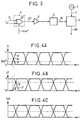
- a first quarter of the diagram Cartesian represents the voltage V of an electrical signal binary modulation as a function of time t
- a second quarter gives the curve C of power P of the optical signal modulated at the output of the electro-absorption modulator in function of the voltage V of the electrical modulation signal
- a third quarter illustrates the power P of the signal optics modulated at the output of the modulator as a function of time t, when the binary electrical modulation signal illustrated in the first quarter is applied to its entrance modulation.
- Binary elements, or bits, of the signal binary electric modulation have a shape substantially trapezoidal, the rising and falling edges of each of these elements being inclined.
- the representation, in the form O2 eye diagram signal envelope modulated optics from the modulator is built by double projection, relative to curve C, of the representation, also in the form of a diagram of eye 01, of the electrical modulation signal.
- the eye O2 diagram of the envelope of the modulated optical signal is asymmetrical, the "fronts" rising and falling of the envelope do not intersecting at a median level of maximum levels Pmax and minimum Pmin of power.
- the invention therefore aims to remedy the drawback above by providing a device particularly advantageous amplitude modulation of an optical signal by a binary electrical signal.
- the electrical signal with N states is a binary electrical signal with 2 states, called prime and second states
- the output of said shaping means switches from the first state to the second state in response to a binary electrical signal level above a threshold predetermined, and switches from the second state to the first state in response to a level of the binary electrical signal below the predetermined threshold.
- the shaping means can be in the form of a door OR with two inputs one of whose inputs receives the binary electrical signal and the other of the inputs of which is set to said first state, the predetermined threshold corresponding to a reference voltage from said OR gate.
- shaping means can also be under the form of a comparator receiving the binary electrical signal on a non-inverting input and receiving the voltage reference on an inverting input.
- the optical signal is produced by a laser source.
- the output of the shaping means can be applied to the second modulator input, of the type electro-absorption modulator, through an amplifier and a polarization tee arranged in series.
- a first input of the electro-absorption modulator 4 receives an optical signal L supplied by the laser source 5.
- a second input of modulator 4 receives a modulating signal M.
- An incoming binary electrical signal S is applied to this second input through the shaping circuit 1, and, possibly the amplifier 2 and the polarization tee 3 arranged in series with the shaping circuit. Tee 3 allows a polarization of the modulator 4 in a zone of proper operation.
- the shaping circuit 1 which is therefore arranged upstream of the second entrance, comprises in cascade an adder 10 and an OR gate with two inputs 11 whose output is connected to the input of the amplifier 2.
- the incoming binary electrical signal S is applied to a first input of the adder 10 including a second input receives a reference voltage Vref.
- An exit from this adder 10 is connected to a first input of OR gate 11.
- a second entry of this gate 11 receives the state "O".
- FIGS. 4A and 4B explain the function of the shaping circuit 1.
- the binary elements in states “1" and "0" are superimposed.
- the output ST of the shaping circuit 1 switches from state “0" to state “1” when the front level amount 6 of the incoming binary signal S is greater than Vref.
- the ST output of the shaping circuit 1 switches from state “1” to state “0” when the level of the falling edge 7 of the incoming binary signal S is less at Vref.
- the rising edges 6 'and falling 7' of the signal ST then have the property of having, in a diagram of the eye diagram type, a point of intersection at a non-median level 8 'while the incoming binary signal S has a point of intersection 8 between rising edges 6 and descendants 7 which is median relative to levels respective corresponding to states "0" and "1".
- the binary electrical signal ST intended for modulate the optical signal L after any amplification 2 and translation 3, has a modified eye diagram at intersected point translated between rising edge and descending, which compensates for the non-linear characteristic of the electro-absorption modulator 4 (FIG.1).
- Figure 4C at the output of the electro-absorption modulator 4, is obtained an eye diagram of the envelope of the substantially symmetrical modulated optical signal which offers, for a given error rate in reception, a maximum distance the signal can travel modulated optics.
- the reference voltage Vref ' must be set to get an eye diagram of the envelope of the substantially modulated optical signal symmetrical.
- This voltage Vref ' is naturally understood between the respective levels associated with states “0" and “1” by being different from these states.
- the setting circuit form can be in the form of a comparator receiving the binary electrical signal entering on a non-inverting input and receiving the reference voltage on a inverting input.
- the invention turns out to be particularly advantageous for high frequencies of the electrical signal incoming binary S, for example equal to 2.5 GHz. She stays nevertheless applicable at any frequency.
- the invention could be extended to modulation by a binary electrical signal with N states. So he is necessary to provide means of shaping including one output switches from one of the N states to another of these N states in response to a higher electrical signal level at a predetermined threshold, and switches from this other state to said one of the states in response to a signal level electric below the predetermined threshold.
- a threshold respective is then associated with each pair of states between which a transition is possible in the signal at N states. This threshold has a level which is between and different from the respective levels taken by the two states considered.
Landscapes
- Engineering & Computer Science (AREA)
- Computer Networks & Wireless Communication (AREA)
- Signal Processing (AREA)
- Physics & Mathematics (AREA)
- Electromagnetism (AREA)
- Optics & Photonics (AREA)
- Optical Communication System (AREA)
Claims (8)
- Vorrichtung zum Amplitudenmodulieren eines optischen Signals (L) mit einem N Zustände aufweisen elektrischen Signal (S), wobei N größer oder gleich 2 ist, mit:wobei die Vorrichtung dadurch gekennzeichnet ist, dass sie vor dem zweiten Eingang eine Formungseinrichtung (1) aufweist, von der ein Eingang das elektrische N-Zustands-Signal (S) empfängt und von der ein Ausgang von einem der N Zustände in einen anderen dieser N Zustände in Reaktion auf ein Niveau des elektrischen.N-Zustands-Signals oberhalb einer vorgegebenen Schwelle (Vref') übergeht und von diesem anderen Zustand zu dem einen der N Zustände in Reaktion auf ein Niveau des elektrischen N-Zustands-Signals unterhalb dieser vorgegebenen Schwelle übergeht, wobei die vorgegebene Schwelle dem Paar aus diesem einen und diesem anderen Zustand zugeordnet ist und ein Niveau hat, das zwischen den jeweiligen von diesen zwei Zuständen eingenommenen Niveaus liegt.einem Modulator (4) zum Empfangen des zu modulierenden optischen Signals (L) auf einem ersten Eingang und einem modulierenden elektrischen Signal (M) auf einem zweiten Eingang,
- Vorrichtung nach Anspruch 1, dadurch gekennzeichnet, dass das elektrische N-Zustands-Signal (S) ein binäres elektrisches Signal mit zwei Zuständen, als erster bzw. zweiter Zustand bezeichnet, ist, und dass der Ausgang der Formungseinrichtung (1) vom ersten Zustand ("0") in den zweiten Zustand ("1") in Reaktion auf ein Niveau des binären elektrischen Signals (S) oberhalb einer vorgegebenen Schwelle (Vref') übergeht und von dem zweiten Zustand ("1") in den ersten Zustand ("0") in Reaktion auf ein Ninveau des binären elektrischen Signals unterhalb der vorgegebenen Schwelle (Vref') übergeht.
- Vorrichtung nach Anspruch 2, dadurch gekennzeichnet, dass die Formungseinrichtung in Form eines Oder-Gatters (12) mit zwei Eingängen vorliegt, wobei der eine der zwei Eingänge das binäre elektrische Signal (S) empfängt und der andere der zwei Eingänge auf den ersten Zustand ("0") gelegt ist, wobei die vorgegebene Schwelle einer Referenzspannung des Oder-Gatters entspricht.
- Vorrichtung nach Anspruch 2, dadurch gekennzeichnet, dass die Formungseinrichtung in Form eines Komparators vorliegt, der das binäre elektrische Signal an einem nicht invertierenden Eingang empfängt und die Referenzspannung an einem invertierenden Eingang empfängt.
- Vorrichtung nach einem beliebigen der vorhergehenden Ansprüche, dadurch gekennzeichnet, dass das optischen Signal von einer Laserquelle (5) erzeugt ist.
- Vorrichtung nach einem beliebigen der vorhergehenden Ansprüche, dadurch gekennzeichnet, dass der Ausgang der Formungseinrichtung auf den zweiten Eingang des Modulators über einen Verstärker (2) gelegt ist.
- Vorrichtung nach einem beliebigen der vorhergehenden Ansprüche, dadurch gekennzeichnet, dass der Ausgang der Formungseinrichtung auf den zweiten Eingang des Modulators über ein Polarisations-T-Stück gelegt ist.
- Vorrichtung nach einem beliebigen der vorhergehenden Ansprüche, dadurch gekennzeichnet, dass der Modulator (4= ein Elektroabsorptionsmodulator ist.
Applications Claiming Priority (2)
| Application Number | Priority Date | Filing Date | Title |
|---|---|---|---|
| FR9512436 | 1995-10-23 | ||
| FR9512436A FR2740285B1 (fr) | 1995-10-23 | 1995-10-23 | Dispositif de modulation d'amplitude a modulateur a electro-absorption |
Publications (2)
| Publication Number | Publication Date |
|---|---|
| EP0771089A1 EP0771089A1 (de) | 1997-05-02 |
| EP0771089B1 true EP0771089B1 (de) | 2002-06-12 |
Family
ID=9483803
Family Applications (1)
| Application Number | Title | Priority Date | Filing Date |
|---|---|---|---|
| EP96402236A Expired - Lifetime EP0771089B1 (de) | 1995-10-23 | 1996-10-21 | Einrichtung zur Amplitudenmodulation mit Elektroabsorptionsmodulator |
Country Status (5)
| Country | Link |
|---|---|
| US (1) | US5724178A (de) |
| EP (1) | EP0771089B1 (de) |
| JP (1) | JPH09181684A (de) |
| DE (1) | DE69621740T2 (de) |
| FR (1) | FR2740285B1 (de) |
Families Citing this family (5)
| Publication number | Priority date | Publication date | Assignee | Title |
|---|---|---|---|---|
| US5822108A (en) * | 1997-06-20 | 1998-10-13 | Sun Microsystems, Inc. | Digital optical power modulator |
| IT1320683B1 (it) * | 2000-10-03 | 2003-12-10 | Marconi Comm Spa | Sistema di trasmissione ottico. |
| EP2896993B1 (de) | 2007-06-13 | 2019-04-24 | Ramot at Tel Aviv University Ltd. | System und Verfahren zur Umwandlung digitaler Daten in ein analoges intensitätsmoduliertes optisches Signal |
| ES2430467B1 (es) * | 2011-03-04 | 2014-08-27 | Universitat Politècnica De Catalunya | Método y aparato para enlace óptico bidireccional con modulación simultánea de amplitud y fase mediante un dispositivo de semiconductor integrado y agnóstico a la longitud de onda. |
| US10623214B1 (en) | 2018-12-01 | 2020-04-14 | Hcl Technologies Limited | System and method for multi-level amplitude modulation and demodulation |
Family Cites Families (8)
| Publication number | Priority date | Publication date | Assignee | Title |
|---|---|---|---|---|
| EP0444688B1 (de) * | 1990-03-01 | 1997-10-08 | Fujitsu Limited | Optischer Sender |
| JP3008608B2 (ja) * | 1991-10-31 | 2000-02-14 | 富士通株式会社 | 電界吸収型光変調器駆動方法 |
| CA2083219C (en) * | 1991-11-19 | 1999-01-05 | Hiroshi Nishimoto | Optical transmitter having optical modulator |
| US5208817A (en) * | 1992-04-10 | 1993-05-04 | At&T Bell Laboratories | Modulator-based lightwave transmitter |
| DE4227097A1 (de) * | 1992-08-17 | 1994-02-24 | Sel Alcatel Ag | Schaltungsanordnung zur Amplitudenmodulation des Ansteuersignals eines Lasers |
| US5321543A (en) * | 1992-10-20 | 1994-06-14 | General Instrument Corporation | Apparatus and method for linearizing an external optical modulator |
| JP3499605B2 (ja) * | 1994-09-07 | 2004-02-23 | 株式会社東芝 | 光外部強度変調器 |
| JPH08316909A (ja) * | 1995-05-16 | 1996-11-29 | Toshiba Corp | 光伝送システム、光送信モジュール、及び光変調器の駆動方法 |
-
1995
- 1995-10-23 FR FR9512436A patent/FR2740285B1/fr not_active Expired - Fee Related
-
1996
- 1996-10-21 DE DE69621740T patent/DE69621740T2/de not_active Expired - Lifetime
- 1996-10-21 EP EP96402236A patent/EP0771089B1/de not_active Expired - Lifetime
- 1996-10-22 US US08/734,604 patent/US5724178A/en not_active Expired - Lifetime
- 1996-10-23 JP JP8281065A patent/JPH09181684A/ja not_active Withdrawn
Also Published As
| Publication number | Publication date |
|---|---|
| US5724178A (en) | 1998-03-03 |
| DE69621740D1 (de) | 2002-07-18 |
| FR2740285A1 (fr) | 1997-04-25 |
| JPH09181684A (ja) | 1997-07-11 |
| FR2740285B1 (fr) | 1997-11-21 |
| DE69621740T2 (de) | 2002-12-19 |
| EP0771089A1 (de) | 1997-05-02 |
Similar Documents
| Publication | Publication Date | Title |
|---|---|---|
| EP0975107B1 (de) | Sendevorrichtung für optische Daten | |
| FR2681203A1 (fr) | Systeme de transmission optique, et emetteur et recepteur optiques. | |
| CA1247231A (fr) | Dispositif pour reduire la dynamique de trois signaux de couleur representant une image | |
| EP0031263A1 (de) | Nichtlineare optische Vorrichtung mit einem zusammengesetzten Lichtwellenleiter und Strahlungsquelle, die eine solche Vorrichtung verwendet | |
| EP0780723B1 (de) | Steuerbarer Amplitude- und Phasenmodulator und Solitonregenerator mit einem solchen Modulator | |
| EP0813097A1 (de) | Vorrichtung zur Formung von digitalen optischen Signalen und ihr Gebrauch zur Veränderung von solchen Signalen | |
| LU81701A1 (fr) | Dispositif de traitement d'un signal d'analyse d'image | |
| EP0771089B1 (de) | Einrichtung zur Amplitudenmodulation mit Elektroabsorptionsmodulator | |
| FR2767202A1 (fr) | Dispositif modulateur optique | |
| FR2759790A1 (fr) | Convertisseur de longueur d'onde de signaux optiques binaires | |
| EP3032325B1 (de) | Vorrichtung zur modulation der amplitude eines optischen signals | |
| CA2093991C (fr) | Source d'impulsion optique et systeme de transmission optique a solitons comportant cette source | |
| EP0744844B1 (de) | Binärdateneinschreibungsverfahren, insbesondere optisches, und Vorrichtung zur Durchführung dieses Verfahrens | |
| EP0022015A1 (de) | Audioverstärker und Verfahren zur Audiofrequenzverstärkung | |
| FR2520174A1 (fr) | Systeme de transmission de signaux numeriques sur fibre optique | |
| CA2266058A1 (fr) | Dispositif de mise en forme de signaux optiques binaires | |
| EP1695465B1 (de) | Rein optischer wandler | |
| FR2717330A1 (fr) | Modulateur semiconducteur électro-optique et liaison optique incluant ce modulateur. | |
| JP2896359B2 (ja) | サブキャリア伝送システム用光変調装置 | |
| EP0746070B1 (de) | Verfahren und Vorrichtung zur Kombination optischer Signale | |
| EP1455451B1 (de) | Vorrichtung zur optischen Signalverarbeitung | |
| JP2869585B2 (ja) | 光変調装置 | |
| CA2338873A1 (fr) | Dispositif d'amplification optique | |
| FR3061783A1 (fr) | Modulateur optique dote de diodes mach-zender de longueur reduite | |
| EP0952624A1 (de) | Elektronische Mehrfachrichtstrahlantenne mit Abtastung |
Legal Events
| Date | Code | Title | Description |
|---|---|---|---|
| PUAI | Public reference made under article 153(3) epc to a published international application that has entered the european phase |
Free format text: ORIGINAL CODE: 0009012 |
|
| AK | Designated contracting states |
Kind code of ref document: A1 Designated state(s): DE DK GB IT |
|
| 17P | Request for examination filed |
Effective date: 19971103 |
|
| GRAG | Despatch of communication of intention to grant |
Free format text: ORIGINAL CODE: EPIDOS AGRA |
|
| 17Q | First examination report despatched |
Effective date: 20011008 |
|
| GRAG | Despatch of communication of intention to grant |
Free format text: ORIGINAL CODE: EPIDOS AGRA |
|
| GRAH | Despatch of communication of intention to grant a patent |
Free format text: ORIGINAL CODE: EPIDOS IGRA |
|
| GRAH | Despatch of communication of intention to grant a patent |
Free format text: ORIGINAL CODE: EPIDOS IGRA |
|
| GRAA | (expected) grant |
Free format text: ORIGINAL CODE: 0009210 |
|
| RAP1 | Party data changed (applicant data changed or rights of an application transferred) |
Owner name: ALCATEL |
|
| AK | Designated contracting states |
Kind code of ref document: B1 Designated state(s): DE DK GB IT |
|
| REG | Reference to a national code |
Ref country code: GB Ref legal event code: FG4D Free format text: NOT ENGLISH |
|
| REF | Corresponds to: |
Ref document number: 69621740 Country of ref document: DE Date of ref document: 20020718 |
|
| PG25 | Lapsed in a contracting state [announced via postgrant information from national office to epo] |
Ref country code: DK Free format text: LAPSE BECAUSE OF FAILURE TO SUBMIT A TRANSLATION OF THE DESCRIPTION OR TO PAY THE FEE WITHIN THE PRESCRIBED TIME-LIMIT Effective date: 20020912 |
|
| PLBE | No opposition filed within time limit |
Free format text: ORIGINAL CODE: 0009261 |
|
| STAA | Information on the status of an ep patent application or granted ep patent |
Free format text: STATUS: NO OPPOSITION FILED WITHIN TIME LIMIT |
|
| 26N | No opposition filed |
Effective date: 20030313 |
|
| PGFP | Annual fee paid to national office [announced via postgrant information from national office to epo] |
Ref country code: IT Payment date: 20101026 Year of fee payment: 15 |
|
| PG25 | Lapsed in a contracting state [announced via postgrant information from national office to epo] |
Ref country code: IT Free format text: LAPSE BECAUSE OF NON-PAYMENT OF DUE FEES Effective date: 20111021 |
|
| PGFP | Annual fee paid to national office [announced via postgrant information from national office to epo] |
Ref country code: GB Payment date: 20131021 Year of fee payment: 18 Ref country code: DE Payment date: 20131021 Year of fee payment: 18 |
|
| REG | Reference to a national code |
Ref country code: DE Ref legal event code: R119 Ref document number: 69621740 Country of ref document: DE |
|
| GBPC | Gb: european patent ceased through non-payment of renewal fee |
Effective date: 20141021 |
|
| PG25 | Lapsed in a contracting state [announced via postgrant information from national office to epo] |
Ref country code: DE Free format text: LAPSE BECAUSE OF NON-PAYMENT OF DUE FEES Effective date: 20150501 Ref country code: GB Free format text: LAPSE BECAUSE OF NON-PAYMENT OF DUE FEES Effective date: 20141021 |