EP0766498B1 - Organische elektrolumineszente Vorrichtungen mit hoher thermischer Stabilität - Google Patents
Organische elektrolumineszente Vorrichtungen mit hoher thermischer Stabilität Download PDFInfo
- Publication number
- EP0766498B1 EP0766498B1 EP19960202574 EP96202574A EP0766498B1 EP 0766498 B1 EP0766498 B1 EP 0766498B1 EP 19960202574 EP19960202574 EP 19960202574 EP 96202574 A EP96202574 A EP 96202574A EP 0766498 B1 EP0766498 B1 EP 0766498B1
- Authority
- EP
- European Patent Office
- Prior art keywords
- organic
- layer
- fluorescent
- aryl
- host
- Prior art date
- Legal status (The legal status is an assumption and is not a legal conclusion. Google has not performed a legal analysis and makes no representation as to the accuracy of the status listed.)
- Expired - Lifetime
Links
- 0 C=*C1C*CC1 Chemical compound C=*C1C*CC1 0.000 description 2
- IYAKXHUZMFATBU-UHFFFAOYSA-N CCN(C)c1ccc(C(c2ccccc2)c(cc2)ccc2N(CC)CC)cc1 Chemical compound CCN(C)c1ccc(C(c2ccccc2)c(cc2)ccc2N(CC)CC)cc1 IYAKXHUZMFATBU-UHFFFAOYSA-N 0.000 description 1
- BRYCXXFBTUXJOK-UHFFFAOYSA-N CN(c(cccc1)c1C1=O)C2=C1N(C)c(cccc1)c1C2=O Chemical compound CN(c(cccc1)c1C1=O)C2=C1N(C)c(cccc1)c1C2=O BRYCXXFBTUXJOK-UHFFFAOYSA-N 0.000 description 1
- GKLACXGCVNIJIX-PKPIPKONSA-N C[C@@H]1C(CCCN)C1 Chemical compound C[C@@H]1C(CCCN)C1 GKLACXGCVNIJIX-PKPIPKONSA-N 0.000 description 1
Images
Classifications
-
- C—CHEMISTRY; METALLURGY
- C09—DYES; PAINTS; POLISHES; NATURAL RESINS; ADHESIVES; COMPOSITIONS NOT OTHERWISE PROVIDED FOR; APPLICATIONS OF MATERIALS NOT OTHERWISE PROVIDED FOR
- C09K—MATERIALS FOR MISCELLANEOUS APPLICATIONS, NOT PROVIDED FOR ELSEWHERE
- C09K11/00—Luminescent, e.g. electroluminescent, chemiluminescent materials
- C09K11/06—Luminescent, e.g. electroluminescent, chemiluminescent materials containing organic luminescent materials
-
- H—ELECTRICITY
- H05—ELECTRIC TECHNIQUES NOT OTHERWISE PROVIDED FOR
- H05B—ELECTRIC HEATING; ELECTRIC LIGHT SOURCES NOT OTHERWISE PROVIDED FOR; CIRCUIT ARRANGEMENTS FOR ELECTRIC LIGHT SOURCES, IN GENERAL
- H05B33/00—Electroluminescent light sources
- H05B33/12—Light sources with substantially two-dimensional radiating surfaces
- H05B33/14—Light sources with substantially two-dimensional radiating surfaces characterised by the chemical or physical composition or the arrangement of the electroluminescent material, or by the simultaneous addition of the electroluminescent material in or onto the light source
Definitions
- This invention relates to organic electroluminescent devices (EL devices). More specifically, this invention relates to devices which emit light from a current conducting organic layer and have high operational stability.
- EL devices organic electroluminescent devices
- organic EL devices Representative of earlier organic EL devices are Gurnee et al U.S. Patent No. 3,172,862, issued March 9, 1965; Gurnee U.S. Patent No. 3,173,050, issued March 9, 1965; Dresner, "Double Injection Electroluminescence in Anthracene", RCA Review, Vol. 30, pp. 322-334, 1969; and Dresner U.S. Patent No. 3,710,167, issued January 9, 1973.
- the organic emitting material was formed of a conjugated organic host material and a conjugated organic activating agent having condensed benzene rings.
- Naphthalene, anthracene, phenanthrene, pyrene, benzopyrene, chrysene, picene, carbazole, fluorene, biphenyl, terpheyls, quarterphenyls, triphenylene oxide, dihalobiphenyl, trans-stilbene, and 1,4-diphenylbutadiene were offered as examples of organic host materials.
- Anthracene, tetracene, and pentacene were named as examples of activating agents.
- the organic emitting material was present as a single layer having thicknesses above 1 mm.
- organic EL device constructions with the organic luminescent medium consisting of two extremely thin layers ( ⁇ 1.0 micrometer in combined thickness) separating the anode and cathode, one specifically chosen to inject and transport holes and the other specifically chosen to inject and transport electrons and also acting as the organic luminescent zone of the device.
- the extremely thin organic luminescent medium offers reduced resistance, permitting higher current densities for a given level of electrical biasing. Since light emission is directly related to current density through the organic luminescent medium, the thin layers coupled with increased charge injection and transport efficiencies have allowed acceptable light emission levels (e.g. brightness levels capable of being visually detected in ambient light) to be achieved with low applied voltages in ranges compatible with integrated circuit drivers, such as field effect-transistors.
- Tang U.S. Patent No. 4,356,429 discloses an EL device formed of an organic luminescent medium consisting of a hole injecting and transporting layer containing a porphyrinic compound and an electron injecting and transporting layer also acting as the luminescent zone of the device.
- VanSlyke et al U.S. Patent No. 4,539,507. VanSlyke et al realized a dramatic improvement in light emission by substituting for the hole injecting and transporting porphyrinic compound of Tang an aromatic tertiary amine layer.
- the organic EL devices have been constructed of a variety of cathode materials. Early investigations employed alkali metals, since these are the lowest work function metals. Tang et al, U.S. Patent No. 4,885,211 discloses an EL device requiring a low voltage to operate and which is comprised of a cathode formed of a plurality of metals other than alkali metals, at least one of which has a work function of less than 4 eV.
- Tang et al in U.S. Patent No. 4,769,292 discloses that the EL device efficiency can be greatly improved by using an organic emitter layer which comprises of a host material and a small amount of dopant molecules.
- a preferred host material is an aluminum complex of 8-hydroxyquinoline, namely tris(8-hydroxyquinolinol) aluminum also commonly known as Alq.
- the dopant molecule is chosen from several classes of highly fluorescent molecules. Perferred examples are the coumarins, rhodamines.
- 5,227,252 another class of molecules useful as dopant in the organic EL device, namely the quinacridone pigment of formula (I): whereR 1 and R 2 are independently hydrogen, methyl group or chlorine or the dehydro form the the quinacridone compound.
- the quinacridone pigment of formula (I) When used with Alq as the host material, highly efficient organic EL device emitting in the green has been disclosed. However, the usefulness of quinacridone as described in formula (I) is limited because of the instability of the quinacridone molecule in EL operation.
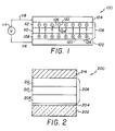
- Figs. 1, 2, and 3 are schematic diagrams of EL devices which can use the present invention.
- An EL device 100 is schematically illustrated in Fig. 1.
- Anode 102 is separated from cathode 104 by an organic luminescent medium 106, which, as shown, consists of three superimposed layers.
- Layer 108 located on the anode forms a hole injecting zone of the organic luminescent medium.
- layer 110 Located above the hole injecting layer is layer 110, which forms a hole transporting zone of the organic luminescent medium.
- layer 112 Interposed between the hole transporting layer and the cathode is layer 112, which forms an electron injecting and transporting zone of the organic luminescent medium.
- the anode and the cathode are connected to an external AC or DC power source 114 by conductors 116 and 118, respectively.
- the power source can be pulsed or continuous wave (CW).
- the EL device can be viewed as a diode which is forward biased when the anode is at a higher potential than the cathode. Under these conditions injection of hole (positive charge carriers) occurs into the lower organic layer, as schematically shown at 120, while electrons are injected into the upper organic layer, as schematically shown at 122, into the luminescent medium. The injected holes and electrons each migrate toward the oppositely charged electrode, as shown by the arrows 124 and 126, respectively. This results in hole-electron recombination. When a migrating electron drops from its conduction potential to a valence band in filing a hole, energy is released as light. Hence the organic luminescent medium forms between the electrodes a luminescence zone receiving mobile charge carriers from each electrode.
- the released light can be emitted from the organic luminescent material through one or more edges 128 of the organic luminescent medium separating the electrodes, through the anode, through the cathode, or through any combination of the foregoing.
- the organic luminescent medium is quite thin, it is usually preferred to emit light through one of the two electrodes. This is achieved by forming the electrodes as a translucent or transparent coating, either on the organic luminescent medium or on a separate translucent or transparent medium or on a separate translucent or transparent support. The thickness of the coating is determined by balancing light transmissions (or extinction) and electrical conductance (or resistance).
- Organic EL device 200 shown in Fig. 2 is illustrative of one preferred embodiment of the invention. Because of the historical development of organic EL devices it is customary to employ a transparent anode. This is achieved by providing a transparent insulative support 202 such as glass onto which is deposited a conductive light transmissive relatively high work function metal or metal oxide layer to form anode 204.
- the organic luminescent medium 206 and therefore each of its layers 208, 210, and 212 correspond to the medium 106 and its layers 108, 110, and 112, respectively, and require no further description. With preferred choices of materials, described below, forming the organic luminescent medium the layer 212 is the zone in which luminescence occurs.
- the cathode 214 is conveniently formed by deposition on the upper layer of the organic luminescent medium.
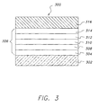
- Organic EL device 300 shown in Figure 3 is illustrative of yet another preferred embodiment of the invention.
- an organic EL device comprised of multilayers of organic thin films 306 sandwiched between anode 304 provided on a glass support 302 and cathode 316.
- a hole-injecting layer 308 On anode 304 is provided a hole-injecting layer 308 that is followed in sequence by a hole-transport layer 310, a doped luminescent layer 312 and an electron-transport layer 314.
- Doped luminescent layer 312 is primarily responsible for the spectral characteristics of the EL device.
- the luminescent zone is in every instance formed by a thin film (herein employed to mean less than 1 ⁇ m in thickness) comprised of an organic host material capable of sustaining hole and electron injection and a fluorescent material capable of emitting light in response to hole-electron recombination. It is preferred that the luminescent zone be maintained in a thickness range of from "5-500 nm (50 to 5000 Angstroms)" and, optimally, "1-100 nm (100 to 1000 Angstroms)", so that the entire organic luminescent medium can be less than 1 ⁇ m and preferably less than "100 nm (1000 Angstroms)" in thickness.
- the host material can be conveniently formed of any material heretofore employed as the active components of a thin film luminescent zone of an organic EL device.
- host materials suitable for use in forming thin films are diarylbutadienes and stilbenes, such as those disclosed by Tang U.S. Patent No. 4,356,429, cited above.
- the organic luminescent medium of the EL devices of this invention contains at least two separate organic layers, one layer forming the electron injecting and transporting zone of the device and one layer forming the hole injecting and transporting zone.
- the former also constitutes the electron-hole recombination and therefore the EL emissive layer.
- Another preferred embodiment of the EL devices of this invention contains a minimum of three separate organic layers, at least one layer forming the electron injecting and transporting zone of the device, and one layer forming the fluorescent emitting layer, and at least one layer forming the hole injecting and transporting zone, where electron-hole recombination and therefore EL emission preferrably takes place in the fluorescent emitting layer.
- a layer containing a porphyrinic compound forms the hole injecting zone of the organic EL device.
- a porphyrinic compound is any compound, natural or synthetic, which is derived from or includes a porphyrin structure, including porphine itself. Any of the prophyrinic compounds disclosed by Adler, U.S. Patent No. 3,935,031 or Tang U.S. Patent No. 4,356,429, can be employed.
- Preferred porphyrinic compounds are those of structural formula (III): wherein
- porphyrinic compounds differ from those of structural formula (I) by substitution of two hydrogens for the metal atom, as indicated by formula (IV):
- porphyrinic compounds are metal free phthalocyanines and metal containing phthalocyanines. While the porphyrinic compounds in general and the phthalocyanines in particular can contain any meal, the metal preferably has a positive valence of two or higher. Exemplary preferred metals are cobalt, magnesium, zinc, palladium, nickel, and, particularly, copper, lead, and platinum.
- the hole transporting layer of the organic EL device contains at least one hole transporting aromatic tertiary amine, where the latter is understood to be a compound containing at least one trivalent nitrogen atom that is bonded only to carbon atoms, at least one of which is a member of an aromatic ring.
- the aromatic tertiary amine can be an arylamine, such as a monarylamine, diarylamine, triarylamine, or a polymeric arylamine. Exemplary monomeric triarylamines are illustrated by Klupfel et al U.S. Patent No. 3,180,730. Other suitable triarylamines substituted with vinyl or vinyl radicals and/or containing at least one active hydrogen containing group are disclosed by Brantley et al U.S. Patent Nos. 3,567,450 and 3,658,520.
- aromatic tertiary amines are those which include at least two aromatic tertiary amine moieties.
- Such compounds include those represented by structural formula (V). wherein
- a preferred class of triarylamines satisfying structural formula (V) and containing two triarylamine moieties are those satisfying structural formula (VI): where
- tetraaryldiamines include two diarylamino groups, such as indicated by formula (VIII), linked through an arylene group: wherein
- the various alkyl, alkylene, aryl, and arylene moieties of the foregoing structural formulae (V), (VI), (VIII), can each in turn be substituted.
- Typical substituents including alkyl groups, alkoxy groups, aryl groups, aryloxy groups, and halogen such as fluoride, chloride, and bromide.
- the various alkyl and alkylene moieties typically contain from about 1 to 6 carbon atoms.
- the cycloalkyl moieties can contain from 3 to about 10 carbon atoms, but typically contain five, six, or seven ring carbon atoms-e.g., cyclopentyl, cyclohexyl, and cycloheptyl ring structures.
- the aryl and arylene moieties are preferably phenyl and phenylene moieties.
- Illustrative of useful hole transport compounds are the following:
- the luminescent zone is in every instance formed by a thin film (herein employed to mean less than 1 ⁇ m in thickness) comprised of an organic host material capable of sustaining hole and electron injection and a fluorescent material capable of emitting light in response to hole-electron recombination. It is preferred that the luminescent zone be maintained in a thickness range of from "5 - 500 nm (50 to 5000 Angstroms)" and, optimally, "10 - 100 nm (100 to 1000 Angstroms)", so that the entire organic luminescent medium can be less than 1 ⁇ m and preferably less than 1000 Angstroms in thickness.
- the host material can be conveniently formed of any material heretofore employed as the active components of a thin film luminescent zone of an organic EL device.
- host materials suitable for use in forming thin films are diarylbutadienes and stilbenes, such as those disclosed by Tang U.S. Patent No. 4,356,429, cited above.
- optical brighteners particularly those disclosed by Van Slyke et al U.S. Patent No. 4,539,507, cited above.
- Useful optical brighteners include those satisfying structural formulae: or wherein:
- aliphatic includes substituted aliphatic as well as unsubstituted aliphatic.
- the substituents in the case of substituted aliphatic include alkyl of from 1 to 5 carbon atoms, for example, methyl, ethyl, propyl and the like; aryl of from 6 to 10 carbon atoms, for example, phenyl and naphthyl; halo, such as chloro, fluoro and the like; nitro; and alkoxy having 1 to 5 carbon atoms, for example, methoxy, ethoxy, propoxy, and the like.
- Still other optical brighteners that are contemplated to be useful are listed in Vol. 5 of Chemistry of Synthetic Dyes, 1971, pages 618-637 and 640. Those that are not already thin-film-forming can be rendered so by attaching an aliphatic moiety to one or both end rings.
- Particularly preferred host materials for forming the luminescent zone of the organic EL devices of this invention are metal chelated oxinoid compounds, including chelates of oxine (also commonly referred to as 8-quinolinol or 8-hydroxyquinoline). Such compounds exhibit both high levels of performance and are readily fabricated in the form of thin films.
- Illustrative of useful host materials including metalized oxines capable of being used to form thin films are the following:
- All of the host materials listed above are known to emit light in response to hole and electron injection.
- a minor amount of a fluorescent material capable of emitting light in response to hole-electron recombination the hue light emitted from the luminescent zone can be modified.
- each material should emit light upon injection of holes and electrons in the luminescent zone. The perceived hue of light emission would be the visual integration of both emissions.
- the fluorescent material Since imposing such a balance of host and fluorescent materials is highly limiting, it is preferred to choose the fluorescent material so that it provides the favored sites for light emission. When only a small proportion of fluorescent material providing favored sites for light emission is present, peak intensity wavelength emissions typical of the host material can be entirely eliminated in favor of a new peak intensity wavelength emission attributable to the fluorescent material. While the minimum proportion of fluorescent material sufficient to achieve this effect varies by the specific choice of host and fluorescent materials, in no instance is it necessary to employ more than about 10 mole percent fluorescent material, based on moles of host material and seldom is it necessary to employ more than 1 mole percent of the fluorescent material.
- any host material capable of emitting light in the absence of fluorescent material limiting the fluorescent material present to extremely small amounts, typically less than about 10 -3 mole percent, based on host material, can result in retaining emission at wavelengths characteristic of the host material.
- a fluorescent material capable of providing favored sites for light emission either a full or partial shifting of emission wavelengths can be realized. This allows the spectral emissions of the EL devices of this invention to be selected and balanced to suit the application to be served.
- Choosing fluorescent materials capable of providing favored sites for light emission necessarily involves relating the properties of the fluorescent material to those of the host material.
- the host material can be viewed as a collector for injected holes and electrons with the fluorescent material providing the molecular sites for light emission.
- One important relationship for choosing a fluorescent material capable of modifying the hue of light emission when present in a host material is a comparison of the reduction potentials of the two materials.
- the fluorescent materials demonstrated to shift the wavelength of light emission have exhibited a less negative reduction potential than that of the host material. Reduction potentials, measured in electron volts, have been widely reported in the literature along with varied techniques for their measurement.
- a second important relationship for choosing a fluorescent material capable of modifying the hue of light emission when present in a host material is a comparison of the bandgap potentials of the two materials.
- the fluorescent materials demonstrated to shift the wavelength of light emission have exhibited a lower bandgap potential than that of the host material.
- the bandgap potential of a molecule is taken as the potential difference in electron volts (eV) separating its ground state and first single state.
- eV electron volts
- Bandgap potentials and techniques for their measurement have been widely reported in the literature.
- the bandgap potentials herein reported are those measured in electron volts (eV) at an absorption wavelength which is bathochromic to the absorption peak and of a magnitude one tenth that of the magnitude of the absorption peak.
- spectral coupling it is meant that an overlap exists between the wavelengths of emission characteristic of the host material alone and the wavelengths of light absorption of the fluorescent material in the absence of the host material.
- Optimal spectral coupling occurs when the maximum emission of the host material alone substantially matches within ⁇ 25 nm the maximum absorption of the fluorescent material alone.
- advantageous spectral coupling can occur with peak emission and absorption wavelengths differing by up to 100 nm or more, depending on the width of the peaks and their hypsochromic and bathochromic slopes.
- a bathochromic as compared to a hypsochromic displacement of the fluorescent material produces more efficient results.
- Useful fluorescent materials are those capable of being blended with the host material and fabricated into thin films satisfying the thickness ranges described above forming the luminescent zones of the EL devices of this invention. While fluorescent materials do not necessarily lend themselves to thin film formation, the limited amounts of these fluorescent materials present in the host materials permits the use of these fluorescent materials which are alone incapable of thin film formation. Preferred fluorescent materials are those which form a common phase with the host material. Although any convenient technique for dispersing the fluorescent materials in the host materials can be undertaken, preferred fluorescent materials are those which can be vacuum vapor deposited along with the host materials.
- the quinacridone compounds disclosed in this invention belong to a class of pigments which are widely used as stable colorants in paints, textiles and automotive industries because of their thermal stability and light fastness. More detailed description of their uses, properties, and preparation methods can be found in Pigment Handbook, edited by Peter A. Lewis, Volume 1, John Wiley & Sons, page 601,
- the use of quinacridone compounds in EL devices have been previously disclosed in U.S. Patent No. 5,227,252. It was found that when the quinacridone compound is dispersed in a host EL material such as Alq by vacuum deposition, the fluorescent efficiency of the resulting mixture is significantly higher than the host Alq material alone. Correspondingly the EL efficiency of the mixture is greatly improved.
- the quinacridone materials disclosed in the above-cited patent specificially refers to compounds of structural formula (I): whereR 1 and R 2 are independently hydrogen, methyl group or chlorine or the dehydro form the the quinacridone compound.
- the quinacridones are known to be highly stable for colorant applications, and are useful in EL application in improving the efficiency, it is not obvious in the latter application that the quinacridones would have operational stability as well.
- the quinacridones of molecular formula (I) have N-H moeities which are capable of forming unstable hydrogen bonds with neigbouring molecules processing carbonyls or other groups. Such an inter-molecular coordination would produce dimers or excited state dimers between adjacent quinacridone molecules which are undesirable for EL operation.
- a preferred thin film forming material for use in forming the electron injecting and transporting layers of the organic EL devices of this invention is metal chelated oxinoid compounds, including chelates of oxine itself (also commonly referred to as 8-quinolinol or 8-hydroxyquinoline). Such compounds exhibit both high levels of performance and are readily fabricated in the form of thin films.
- exemplary of contemplated oxinoid compounds are those satisfying structural formula (IX).
- the metal can be monovalent, divalent, or trivalent metal.
- the metal can, for example, be an alkali metal, such as lithium, sodium, or potassium; an alkaline earth metal, such as magnesium or calcium; or an earth metal, such as boron or aluminum.
- any monovalent, divalent, or trivalent metal known to be a useful chelating metal can be employed.
- Z completes a heterocyclic nucleus containing at least two fused aromatic rings, at least one of which is an azole or azine ring. Additional rings, including both aliphatic and aromatic rings, can be fused with the two required rings, if required. To avoid adding molecular bulk without improving on function the number of ring atoms is preferably maintained at 18 or less.
- Illustrative of useful chelated oxinoid compounds are the following:
- the organic EL devices of the invention it is possible to maintain a current density compatible with efficient light emission while employing a relatively low voltage across the electrodes by limiting the total thickness of the organic luminescent medium to less than "1000 nm" .
- an applied voltage of 20 volts results in a field potential of greater than 2 x 10 5 volts/cm, which is compatible with efficient light emission.
- An order of magnitude reduction to 10 nm in thickness of the organic luminescent medium, allowing further reductions in applied voltage and/or increase in the field potential and hence current density, are well within device construction capabilities.
- the preferred materials for forming the organic luminescent medium are each capable of fabrication in the form of a thin film-that is, capable of being fabricated as a continuous layer having a thickness of less than 500 nm.
- a preferred method for forming the organic luminescent medium is by vacuum vapor deposition. Extremely thin defect free continuous layers can be formed by this method. Specifically, individual layer thicknesses as low as about 5 nm can be constructed while still realizing satisfactory EL device performance.
- a vacuum vapor deposited porphorinic compound as a hole injecting layer
- a film forming aromatic tertiary amine as a hole transporting layer
- a fluorescent emitting layer comprised of a mixture of a host material and a fluorescent compound
- a chelated oxinoid compound as an electron injecting and transporting layer
- individual layer thicknesses in the range of from about "5 - 500" nm are contemplated, with layer thicknesses in the range of from "10 - 200" nm being preferred. It is generally preferred that the overall thickness of the organic luminescent medium be at least about 100 nm.
- the anode and cathode of the organic EL device can each take any convenient conventional form. Where it is intended to transmit light from the organic EL device through the anode, this can be conveniently achieved by coating a thin conductive layer onto a light transmissive substrate ⁇ e.g., a transparent or substantially transparent glass plate or plastic film.
- a light transmissive substrate e.g., a transparent or substantially transparent glass plate or plastic film.
- the organic EL devices of this invention can follow the historical practice of including a light transmissive anode formed of tin oxide or indium tin oxide coated on a glass plate, as disclosed by Gurnee et al U.S. Patent No. 3,172,862, Gurnee U.S. Patent No. 3,173,050, Dresner "Double Injection Electroluminescence in Anthracene", RCA Review , Volume 30, pages 322-334, 1969; and Dresner U.S. Patent No. 3,710,167 cited above.
- the organic EL devices of this invention can employ a cathode constructed of any metal, including any high or low work function metal, heretofore taught to be useful for this purpose.
- a cathode constructed of any metal, including any high or low work function metal, heretofore taught to be useful for this purpose.
- Unexpected fabrication, performance, and stability advantages have been realized by forming the cathode of a combination of a low work function metal and at least one other metal.
- U.S. Patent No. 4,885,211 by Tang and VanSlyke see U.S. Patent No. 4,885,211 by Tang and VanSlyke.
- the device structure has a four organic-layer stack, namely hole-injecting layer, hole transporting layer, fluorescent emitting layer, electron-transporting layer.
- the above sequence completed the deposition of the EL device.
- the device was then hermetically parckaged in a dry glove box for protection against ambient environment.
- Example 3 - EL devices with N,N dimethyl quinacridone doped Alq fluorescent emitter layer
- the EL devices were fabricated according to the procedure of Example 2.
- the fluorescent emitting layer was Alq doped with various concentration of N,N'-dimethylquinacridone.
- Table 1 lists the luminance quantum efficiency measured in unit of candela per ampere, and CIE color coordinates and the luminance output under a constant current bias of 20mA/cm ⁇ 2.
- Luminance Performance of EL devices with N,N'-dimethylquinacridone doped Alq fluorescent emitting layer EL Parameters Concentration of dopant in Alq host Dopant concentration 0% 0.26% 0.80% 1.40% 2.50% Luminance(Cd/M ⁇ 2) 518 1147 1462 1287 1027 CIE-x 0.385 0.387 0.392 0.404 0.409 CIE-y 0.546 0.586 0.590 0.580 0.574 Luminance Eff. (cd/A) 2.59 5.736 7.31 6.435 5.135
- Example 4 Operational stability of EL devices with N,N dimethyl quinacridone doped Alq fluorescent emitter layer
- the operational stability of the El device was tested under an AC bias condition with a time averaged forward bias current density of 20 mA/cm ⁇ 2.
- the AC waveform was square and the frequency was 1 kHz.
- a constant current was impressed upon the device; in the reverse cycle, a constant voltage of 14 volts.
- Table 2 summarizes the stability performance of the set of EL devices of Example 2. This table lists the relative luminance level of the EL devices at various time intervals. The absolute luminance at initial times is listed in Table 1.
- the EL devices were fabricated according to the procedure of Example 2.
- the fluorescent emitting layer was Alq doped with various concentration of quinacridone.
- Table 3 lists the luminance quantum efficiency measured in unit of candela per ampere, and CIE color coordinates and the luminance output under a constant current bias of 20mA/cm ⁇ 2.
- Luminance Performance of EL devices with unsubstituted quinacridone doped Alq fluorescent emitting layer EL Parameters Concentration of dopant in Alq host Dopant concentration 0% 0.20% 0.40% 0.80% 1.40% Luminance (Cd/M ⁇ 2) 558 1180 1205 1657 1494 CIE-x 0.344 0.367 0.403 0.386 0.395 CIE-y 0.556 0.590 0.580 0.593 0.593 Luminance Eff. (cd/A) 2.79 5.90 7.31 8.285 7.47
- the operational stability of the El device was tested under an AC bias condition with a time averaged forward bias current density of 20 mA/cm ⁇ 2.
- the AC waveform was square and the frequency was 1 kHz.
- a constant current was impressed upon the device; in the reverse cycle, a constant voltage of 14 volts.
- Table 4 summarizes the stability performance of the set of EL devices of Example 5.
- the table lists the relative luminance level of the EL devices at various time intervals. The absolute luminance at initial times is listed in Table 3.
Claims (5)
- Eine organische elektroluminiszente Vorrichtung, die eine Anode und Kathode sowie ein zwischen Anode und Kathode angeordnetes organisches elektroluminiszentes Element aufweist,
gekennzeichnet dadurch, daß das organische elektroluminiszente Element mindestens eine fluoreszente emittierende Lage oder Schicht aufweist, die eine Mischung von zwei oder mehr Materialien enthält; wobei die Mischung eine Verbindung mit der folgenden Formel enthält:wobei R3 und R4 unabhängig folgendes sind: Alkyl, Akoxyl, substituiertes Alkyl, Aryl, kondensiertes Aryl-Halogen; und R5 und R6 sind unabhängig Alkyl, Alkoxyl, substituiertes Alkyl, Aryl, oder substituiertes Aryl; und n=0,1,2 oder 3.
- Eine organische elektroluminiszente Vorrichtung nach Anspruch 1, wobei die Mischung einen Metallkomplex der folgenden Formel enthält:wobei
 Me ein Metall repräsentiert;n eine ganze Zahl von 1 bis 3 ist; undZ unabhängig für jedes Auftreten die Atome repräsentiert die einen Kern mit mindestens zwei kondensierten aromatischen Ringen komplimentieren.
 - Eine organische elektroluminiszente Vorrichtung nach Anspruch 1, wobei R5 und R6 Methyl, Ethyl oder Phenyl sind.
- Eine organische elektroluminiszente Vorrichtung nach Anspruch 1, wobei R3 und R4 Wasserstoff und R5 und R6 Methyl oder tertiäres Butyl sind.
- Eine organische elektroluminiszente Vorrichtung nach Anspruch 1, wobei die Mischung Alq enthält.
Applications Claiming Priority (4)
| Application Number | Priority Date | Filing Date | Title |
|---|---|---|---|
| US450895P | 1995-09-29 | 1995-09-29 | |
| US4508 | 1995-09-29 | ||
| US08/637,987 US5593788A (en) | 1996-04-25 | 1996-04-25 | Organic electroluminescent devices with high operational stability |
| US637987 | 1996-04-25 |
Publications (3)
| Publication Number | Publication Date |
|---|---|
| EP0766498A2 EP0766498A2 (de) | 1997-04-02 |
| EP0766498A3 EP0766498A3 (de) | 1997-07-09 |
| EP0766498B1 true EP0766498B1 (de) | 2001-01-24 |
Family
ID=26673095
Family Applications (1)
| Application Number | Title | Priority Date | Filing Date |
|---|---|---|---|
| EP19960202574 Expired - Lifetime EP0766498B1 (de) | 1995-09-29 | 1996-09-16 | Organische elektrolumineszente Vorrichtungen mit hoher thermischer Stabilität |
Country Status (3)
| Country | Link |
|---|---|
| EP (1) | EP0766498B1 (de) |
| JP (1) | JPH09176630A (de) |
| DE (1) | DE69611647T2 (de) |
Families Citing this family (8)
| Publication number | Priority date | Publication date | Assignee | Title |
|---|---|---|---|---|
| DE19627070A1 (de) | 1996-07-05 | 1998-01-08 | Bayer Ag | Elektrolumineszierende Anordnungen unter Verwendung von Blendsystemen |
| DK0968254T3 (da) | 1997-02-03 | 2004-12-06 | Ciba Sc Holding Ag | Fluorescerende materialer og deres anvendelse |
| JP3781520B2 (ja) * | 1997-08-26 | 2006-05-31 | 三井化学株式会社 | 有機電界発光素子 |
| DE19803889A1 (de) | 1998-01-31 | 1999-08-05 | Bosch Gmbh Robert | Elektrolumineszierende Anordnung unter Verwendung von dotierten Blendsystemen |
| US6392250B1 (en) * | 2000-06-30 | 2002-05-21 | Xerox Corporation | Organic light emitting devices having improved performance |
| GB0103011D0 (en) * | 2001-02-07 | 2001-03-21 | Clariant Int Ltd | Improvements in or relating to chemical compounds |
| US20090057613A1 (en) * | 2004-06-29 | 2009-03-05 | Ciba Specialty Chemicals Holding Inc. | Fluorescent quinacridones |
| JP2018145109A (ja) * | 2017-03-01 | 2018-09-20 | Jnc株式会社 | 多環芳香族化合物、多環芳香族化合物の多量体、それらの製造方法、およびそれらを含む有機半導体デバイス |
Family Cites Families (4)
| Publication number | Priority date | Publication date | Assignee | Title |
|---|---|---|---|---|
| JP2815472B2 (ja) * | 1990-01-22 | 1998-10-27 | パイオニア株式会社 | 電界発光素子 |
| JP2974835B2 (ja) * | 1991-09-12 | 1999-11-10 | パイオニア株式会社 | 有機エレクトロルミネッセンス素子 |
| EP0569827A2 (de) * | 1992-05-11 | 1993-11-18 | Idemitsu Kosan Company Limited | Organische elektrolumineszente Vorrichtung |
| GB9418495D0 (en) * | 1994-09-14 | 1994-11-02 | Ciba Geigy Ag | Mono-n-alkyl-quinacridone pigments |
-
1996
- 1996-09-16 DE DE1996611647 patent/DE69611647T2/de not_active Expired - Lifetime
- 1996-09-16 EP EP19960202574 patent/EP0766498B1/de not_active Expired - Lifetime
- 1996-09-26 JP JP8254956A patent/JPH09176630A/ja active Pending
Also Published As
| Publication number | Publication date |
|---|---|
| DE69611647D1 (de) | 2001-03-01 |
| DE69611647T2 (de) | 2001-08-16 |
| JPH09176630A (ja) | 1997-07-08 |
| EP0766498A3 (de) | 1997-07-09 |
| EP0766498A2 (de) | 1997-04-02 |
Similar Documents
| Publication | Publication Date | Title |
|---|---|---|
| US5593788A (en) | Organic electroluminescent devices with high operational stability | |
| US6020078A (en) | Green organic electroluminescent devices | |
| EP0825804B1 (de) | Blauorganische Elektrolumineszenzvorrichtungen | |
| US5766779A (en) | Electron transporting materials for organic electroluminescent devices | |
| EP0786925B1 (de) | Weiss-ausstrahlende organische Elektrolumineszenzvorrichtungen | |
| US5928802A (en) | Efficient blue organic electroluminescent devices | |
| US5908581A (en) | Red organic electroluminescent materials | |
| US5935720A (en) | Red organic electroluminescent devices | |
| US5409783A (en) | Red-emitting organic electroluminescent device | |
| EP0120673B1 (de) | Organische elektrolumineszente Vorrichtungen mit Leistungen der Umwandlungsfähigkeit | |
| KR100843826B1 (ko) | 개선된 휘도 효율을 갖는 유기 발광 다이오드 장치 | |
| EP0857007B1 (de) | Organische elektrolimineszente vorrichtung | |
| US5932363A (en) | Electroluminescent devices | |
| US5276381A (en) | Organic electroluminescent device | |
| EP0468437B1 (de) | Elektrolumineszente Vorrichtung mit verbesserter Kathode | |
| EP0647694B1 (de) | Organische elektroluminineszente elementen | |
| EP0525739B1 (de) | Organisches elektrolumineszierendes Gerät (I) mit innerem Übergang von verbesserter Blau-Emission | |
| EP0766498B1 (de) | Organische elektrolumineszente Vorrichtungen mit hoher thermischer Stabilität | |
| JP3871396B2 (ja) | 有機el素子 | |
| EP1009042A2 (de) | Elektrolumineszente Vorrichtung mit Arylethylenderivate in der Ladungslöchertransportschicht | |
| US20030099861A1 (en) | Efficient red organic electroluminescent devices |
Legal Events
| Date | Code | Title | Description |
|---|---|---|---|
| PUAI | Public reference made under article 153(3) epc to a published international application that has entered the european phase |
Free format text: ORIGINAL CODE: 0009012 |
|
| AK | Designated contracting states |
Kind code of ref document: A2 Designated state(s): DE FR GB |
|
| PUAL | Search report despatched |
Free format text: ORIGINAL CODE: 0009013 |
|
| AK | Designated contracting states |
Kind code of ref document: A3 Designated state(s): DE FR GB |
|
| 17P | Request for examination filed |
Effective date: 19980108 |
|
| GRAG | Despatch of communication of intention to grant |
Free format text: ORIGINAL CODE: EPIDOS AGRA |
|
| 17Q | First examination report despatched |
Effective date: 20000301 |
|
| GRAG | Despatch of communication of intention to grant |
Free format text: ORIGINAL CODE: EPIDOS AGRA |
|
| GRAH | Despatch of communication of intention to grant a patent |
Free format text: ORIGINAL CODE: EPIDOS IGRA |
|
| GRAH | Despatch of communication of intention to grant a patent |
Free format text: ORIGINAL CODE: EPIDOS IGRA |
|
| GRAA | (expected) grant |
Free format text: ORIGINAL CODE: 0009210 |
|
| AK | Designated contracting states |
Kind code of ref document: B1 Designated state(s): DE FR GB |
|
| REF | Corresponds to: |
Ref document number: 69611647 Country of ref document: DE Date of ref document: 20010301 |
|
| ET | Fr: translation filed | ||
| PLBE | No opposition filed within time limit |
Free format text: ORIGINAL CODE: 0009261 |
|
| STAA | Information on the status of an ep patent application or granted ep patent |
Free format text: STATUS: NO OPPOSITION FILED WITHIN TIME LIMIT |
|
| REG | Reference to a national code |
Ref country code: GB Ref legal event code: IF02 |
|
| 26N | No opposition filed | ||
| REG | Reference to a national code |
Ref country code: FR Ref legal event code: TP |
|
| REG | Reference to a national code |
Ref country code: GB Ref legal event code: 732E Free format text: REGISTERED BETWEEN 20110224 AND 20110302 |
|
| REG | Reference to a national code |
Ref country code: FR Ref legal event code: PLFP Year of fee payment: 20 |
|
| PGFP | Annual fee paid to national office [announced via postgrant information from national office to epo] |
Ref country code: GB Payment date: 20150916 Year of fee payment: 20 Ref country code: DE Payment date: 20150908 Year of fee payment: 20 |
|
| PGFP | Annual fee paid to national office [announced via postgrant information from national office to epo] |
Ref country code: FR Payment date: 20150811 Year of fee payment: 20 |
|
| REG | Reference to a national code |
Ref country code: DE Ref legal event code: R071 Ref document number: 69611647 Country of ref document: DE |
|
| REG | Reference to a national code |
Ref country code: GB Ref legal event code: PE20 Expiry date: 20160915 |
|
| PG25 | Lapsed in a contracting state [announced via postgrant information from national office to epo] |
Ref country code: GB Free format text: LAPSE BECAUSE OF EXPIRATION OF PROTECTION Effective date: 20160915 |