EP0647694B1 - Organische elektroluminineszente elementen - Google Patents
Organische elektroluminineszente elementen Download PDFInfo
- Publication number
- EP0647694B1 EP0647694B1 EP19940910036 EP94910036A EP0647694B1 EP 0647694 B1 EP0647694 B1 EP 0647694B1 EP 19940910036 EP19940910036 EP 19940910036 EP 94910036 A EP94910036 A EP 94910036A EP 0647694 B1 EP0647694 B1 EP 0647694B1
- Authority
- EP
- European Patent Office
- Prior art keywords
- layer
- transport
- hole
- organic electroluminescent
- electroluminescent element
- Prior art date
- Legal status (The legal status is an assumption and is not a legal conclusion. Google has not performed a legal analysis and makes no representation as to the accuracy of the status listed.)
- Expired - Lifetime
Links
Images


Classifications
-
- H—ELECTRICITY
- H05—ELECTRIC TECHNIQUES NOT OTHERWISE PROVIDED FOR
- H05B—ELECTRIC HEATING; ELECTRIC LIGHT SOURCES NOT OTHERWISE PROVIDED FOR; CIRCUIT ARRANGEMENTS FOR ELECTRIC LIGHT SOURCES, IN GENERAL
- H05B33/00—Electroluminescent light sources
- H05B33/12—Light sources with substantially two-dimensional radiating surfaces
- H05B33/14—Light sources with substantially two-dimensional radiating surfaces characterised by the chemical or physical composition or the arrangement of the electroluminescent material, or by the simultaneous addition of the electroluminescent material in or onto the light source
-
- C—CHEMISTRY; METALLURGY
- C09—DYES; PAINTS; POLISHES; NATURAL RESINS; ADHESIVES; COMPOSITIONS NOT OTHERWISE PROVIDED FOR; APPLICATIONS OF MATERIALS NOT OTHERWISE PROVIDED FOR
- C09K—MATERIALS FOR MISCELLANEOUS APPLICATIONS, NOT PROVIDED FOR ELSEWHERE
- C09K11/00—Luminescent, e.g. electroluminescent, chemiluminescent materials
- C09K11/06—Luminescent, e.g. electroluminescent, chemiluminescent materials containing organic luminescent materials
-
- H—ELECTRICITY
- H05—ELECTRIC TECHNIQUES NOT OTHERWISE PROVIDED FOR
- H05B—ELECTRIC HEATING; ELECTRIC LIGHT SOURCES NOT OTHERWISE PROVIDED FOR; CIRCUIT ARRANGEMENTS FOR ELECTRIC LIGHT SOURCES, IN GENERAL
- H05B33/00—Electroluminescent light sources
- H05B33/12—Light sources with substantially two-dimensional radiating surfaces
-
- H—ELECTRICITY
- H10—SEMICONDUCTOR DEVICES; ELECTRIC SOLID-STATE DEVICES NOT OTHERWISE PROVIDED FOR
- H10K—ORGANIC ELECTRIC SOLID-STATE DEVICES
- H10K50/00—Organic light-emitting devices
- H10K50/10—OLEDs or polymer light-emitting diodes [PLED]
- H10K50/11—OLEDs or polymer light-emitting diodes [PLED] characterised by the electroluminescent [EL] layers
-
- H—ELECTRICITY
- H10—SEMICONDUCTOR DEVICES; ELECTRIC SOLID-STATE DEVICES NOT OTHERWISE PROVIDED FOR
- H10K—ORGANIC ELECTRIC SOLID-STATE DEVICES
- H10K85/00—Organic materials used in the body or electrodes of devices covered by this subclass
- H10K85/10—Organic polymers or oligomers
- H10K85/111—Organic polymers or oligomers comprising aromatic, heteroaromatic, or aryl chains, e.g. polyaniline, polyphenylene or polyphenylene vinylene
-
- H—ELECTRICITY
- H10—SEMICONDUCTOR DEVICES; ELECTRIC SOLID-STATE DEVICES NOT OTHERWISE PROVIDED FOR
- H10K—ORGANIC ELECTRIC SOLID-STATE DEVICES
- H10K85/00—Organic materials used in the body or electrodes of devices covered by this subclass
- H10K85/10—Organic polymers or oligomers
- H10K85/141—Organic polymers or oligomers comprising aliphatic or olefinic chains, e.g. poly N-vinylcarbazol, PVC or PTFE
- H10K85/146—Organic polymers or oligomers comprising aliphatic or olefinic chains, e.g. poly N-vinylcarbazol, PVC or PTFE poly N-vinylcarbazol; Derivatives thereof
-
- H—ELECTRICITY
- H10—SEMICONDUCTOR DEVICES; ELECTRIC SOLID-STATE DEVICES NOT OTHERWISE PROVIDED FOR
- H10K—ORGANIC ELECTRIC SOLID-STATE DEVICES
- H10K85/00—Organic materials used in the body or electrodes of devices covered by this subclass
- H10K85/30—Coordination compounds
- H10K85/321—Metal complexes comprising a group IIIA element, e.g. Tris (8-hydroxyquinoline) gallium [Gaq3]
- H10K85/324—Metal complexes comprising a group IIIA element, e.g. Tris (8-hydroxyquinoline) gallium [Gaq3] comprising aluminium, e.g. Alq3
-
- H—ELECTRICITY
- H10—SEMICONDUCTOR DEVICES; ELECTRIC SOLID-STATE DEVICES NOT OTHERWISE PROVIDED FOR
- H10K—ORGANIC ELECTRIC SOLID-STATE DEVICES
- H10K85/00—Organic materials used in the body or electrodes of devices covered by this subclass
- H10K85/60—Organic compounds having low molecular weight
- H10K85/631—Amine compounds having at least two aryl rest on at least one amine-nitrogen atom, e.g. triphenylamine
-
- H—ELECTRICITY
- H10—SEMICONDUCTOR DEVICES; ELECTRIC SOLID-STATE DEVICES NOT OTHERWISE PROVIDED FOR
- H10K—ORGANIC ELECTRIC SOLID-STATE DEVICES
- H10K85/00—Organic materials used in the body or electrodes of devices covered by this subclass
- H10K85/60—Organic compounds having low molecular weight
- H10K85/649—Aromatic compounds comprising a hetero atom
- H10K85/656—Aromatic compounds comprising a hetero atom comprising two or more different heteroatoms per ring
- H10K85/6565—Oxadiazole compounds
-
- Y—GENERAL TAGGING OF NEW TECHNOLOGICAL DEVELOPMENTS; GENERAL TAGGING OF CROSS-SECTIONAL TECHNOLOGIES SPANNING OVER SEVERAL SECTIONS OF THE IPC; TECHNICAL SUBJECTS COVERED BY FORMER USPC CROSS-REFERENCE ART COLLECTIONS [XRACs] AND DIGESTS
- Y02—TECHNOLOGIES OR APPLICATIONS FOR MITIGATION OR ADAPTATION AGAINST CLIMATE CHANGE
- Y02B—CLIMATE CHANGE MITIGATION TECHNOLOGIES RELATED TO BUILDINGS, e.g. HOUSING, HOUSE APPLIANCES OR RELATED END-USER APPLICATIONS
- Y02B20/00—Energy efficient lighting technologies, e.g. halogen lamps or gas discharge lamps
-
- Y—GENERAL TAGGING OF NEW TECHNOLOGICAL DEVELOPMENTS; GENERAL TAGGING OF CROSS-SECTIONAL TECHNOLOGIES SPANNING OVER SEVERAL SECTIONS OF THE IPC; TECHNICAL SUBJECTS COVERED BY FORMER USPC CROSS-REFERENCE ART COLLECTIONS [XRACs] AND DIGESTS
- Y10—TECHNICAL SUBJECTS COVERED BY FORMER USPC
- Y10S—TECHNICAL SUBJECTS COVERED BY FORMER USPC CROSS-REFERENCE ART COLLECTIONS [XRACs] AND DIGESTS
- Y10S428/00—Stock material or miscellaneous articles
- Y10S428/917—Electroluminescent
-
- Y—GENERAL TAGGING OF NEW TECHNOLOGICAL DEVELOPMENTS; GENERAL TAGGING OF CROSS-SECTIONAL TECHNOLOGIES SPANNING OVER SEVERAL SECTIONS OF THE IPC; TECHNICAL SUBJECTS COVERED BY FORMER USPC CROSS-REFERENCE ART COLLECTIONS [XRACs] AND DIGESTS
- Y10—TECHNICAL SUBJECTS COVERED BY FORMER USPC
- Y10T—TECHNICAL SUBJECTS COVERED BY FORMER US CLASSIFICATION
- Y10T428/00—Stock material or miscellaneous articles
- Y10T428/31504—Composite [nonstructural laminate]
- Y10T428/31678—Of metal
Definitions
- the present invention relates to organic electroluminescent (EL) elements.
- an organic electroluminescent element is caused by a phenomenon where holes and electrons injected from electrode are recombined within a luminescent layer to generate excitons, and the excitons excite molecules of luminescent materials constituting the luminescent layer.
- fluorescent dye as a luminescent material, there can be obtained an emission spectrum, as an electroluminescence, being equivalent to photoluminescence of the dye molecules.
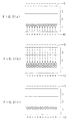
- Tang and Vanslyke recently proposed an element comprising two layers of a hole-transport layer and an electron-transport luminescent layer which efficiently emits green light at a lower voltage of about 10 V compared with a conventional organic electroluminescent element of a single-layer structure [C.W. Tang and S.A. Vanslyke; Appl. Phys. Lett., 51 (1987) 913].
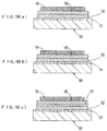
- This element's structure is, as shown in Fig. 19 (a) , composed of an anode 91 , a hole-transport layer 92 , an electron-transport luminescent layer 93 and a cathode 94 , which are formed in this order on a glass substrate 90 .
- the hole-transport layer 92 not only allows holes to be injected from the anode 91 into the electron-transport luminescent layer 93 , but prevents electrons injected from the cathode 94 from escaping into the anode 91 without recombining with the holes, so that the electrons are contained into the electron-transport luminescent layer 93 .
- the electron containment effect due to the hole-transport layer 92 facilitates the recombination of the holes and the electrons compared with the conventional single-layer structure element, resulting in a substantial decrease in drive voltage.
- the two-layer structure element of Saito et al. is, as shown in Fig. 19 (b) , composed of an anode 91 , a hole-transport luminescent layer 95 , an electron-transport layer 96 and a cathode 94 , which are formed in this order on a glass substrate 90 .
- the electron-transport layer 96 not only allow electrons to be injected from the cathode 94 into the hole-transport luminescent layer 95 , but prevents the holes injected from the anode 91 from escaping into the cathode 94 avoiding the recombination with the electrons, so that the holes are contained into the hole-transport luminescent layer 95 .
- This hole containment effect due to the electron-transport layer 96 realizes a substantial decrease in drive voltage likewise in the previous element.
- the three-layer structure element of Saito et al. was attained by a further improvement in the element of Tang et al.
- this element is composed of an anode 91 , a hole-transport layer 92 , a luminescent layer 97 , an electron-transport layer 96 and a cathode 94 , which are formed in this order on a glass substrate 90 .
- the hole-transport layer 92 contains electrons into the luminescent layer 97
- the electron-transport layer 96 contains holes into the luminescent layer 97 , so that the recombination of the electrons and the holes in the luminescent layer 97 is more efficient than the two-layer structure element.
- the electron-transport layer 96 and the hole-transport layer 92 prevent excitons generated by the above recombination from escaping into either an anode or a cathode. Therefore, the three-layer structure element of Saito et al. increases luminous efficiency furthermore.
- Examples of hole-transport material which constitute the above organic electroluminescent elements are aromatic tertiary amines such as triphenylamine.
- Examples of electron-transport material are oxadiazoles.
- Examples of luminescent material are tetraphenybutadiene derivatives, tris(8-quinolinolato)aluminum (III) complex, distyrylbenzene derivatives, distyrylbiphenyl derivatives.
- organic electroluminescent elements are that they can emit light of high luminance at a lower voltage than a conventional electroluminescent element employing inorganic luminescent material, and that they can easily increase the surface area because the respective layers can be formed not only by vacuum deposition but solution application, and that they can emit light of multi-color depending upon molecular design for organic molecule.
- Each element however, has the disadvantage that luminance decrease significantly with a long-term emission. It is therefore the urgent problems to improve stability and to extend the life.
- the conventional electroluminescent elements have the disadvantage that it is difficult to emit blue light irrespective of organic/inorganic or single/plural layer.
- the inorganic element has a problem that an inorganic light emission material with a wide band gap required for blue light emission is limited. Moreover, such a material is often accompanied by technical difficulties in crystal growth or thin film production, thereby making it difficult to produce an element from this material.
- every conventional electroluminescent element is for a single color light emission. It is therefore impossible at present to realize, by using one element, light emission of more than two mutually different spectrums which enables a multi-color display due to three primary color emissions: R (Red); G (Green); and B (Blue), and white light emission.
- Ogura et al. proposed a three-layer structure element employing a bis-di(p-tolyl)aminophenyl-l,l-cyclohexane as a diamine derivative for a hole-transport layer, a 1,1-di(p-methoxyphenyl)-4,4-diphenylbutadiene as a tetraphenylbutadiene derivative for a luminescent layer and a 2-(4-biphenylyl)-5-(4-tert-butylphenyl)-1,3,4-oxadiazole as an oxadiazole derivative for an electron-transport layer [Sharp Technical Journal, 52 (3), 15-18 (1992)].
- This element has a peak of emission spectrum at wavelengths of 480 nm and 590 nm, and emits white light.
- the light having the wavelength of 480 nm is due to the luminescent layer having hole-transport properties, while that having a wavelength of 590 nm is due to the hole-transport layer.
- Ogura et al. described that the mechanism of light emission from the hole-transport layer is based on diffusion of excitons from the luminescent layer.
- Mori et al. proposed an organic electroluminescent element comprising a single luminescent layer, wherein luminescent material such as a coumarin 6 and a coumarin 7 being known as a laser dye, and an oxadiazole derivative as an electron-transport material are molecularly dispersed in a high-molecular poly-N-vinyl carbazol which serves as a hole-transport material and a resin binder. It is their opinion that various color light emissions are available by selecting the kind of dye to be molecularly dispersed in the luminescent layer [Oyo Buturi 61 (10), 1044-1047 (1992)].
- This element may realize a multi-color display due to three primary colors of R, G and B or white light emission by selecting the dye kind and the dye combination.
- the three-layer structure element of Ogura has the disadvantage of being unstable due to a large drop in luminescent intensity during the use. It appears that this instability is caused by deterioration, coagulation or crystallization due to heat release when the element emits light.
- the recombination of the holes and the electrons is insufficient and its luminance is low because of being a single-layer.
- the first organic electroluminescent element of the present invention comprises at least one layer of a 1,2,4-triazole derivative.
- the low-molecular 1,2,4-triazole derivative (the term "low-molecular” used herein is not shown by molecular weight, but means that it has no main chain structure like a high-molecular 1,2,4-triazole derivative described later) have never been employed as an organic electroluminescent material until the present inventors do so.
- the 1,2,4-triazole derivative is not valid for a hole-transport material, if employed as an electron-transport material, it presents electron-transport properties and hole-blocking properties superior to those of other conventional materials.
- the efficiency of the recombination of electron and holes increases and that of containment of excitons generated by the above combination increases, both contributing a further increase in luminous efficiency, luminance of the luminescent layer and stability accompanied thereby.
- the combination of this derivative and a conventional luminescent layer for blue light emission which has high hole-transport properties can raise luminous efficiency and luminance to a required level for practical applications. This realizes such blue light emission having high luminance as previously described.
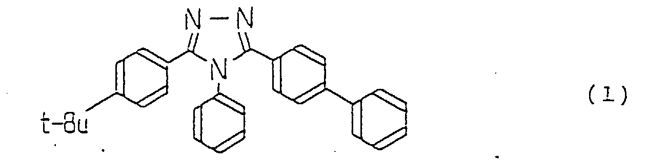
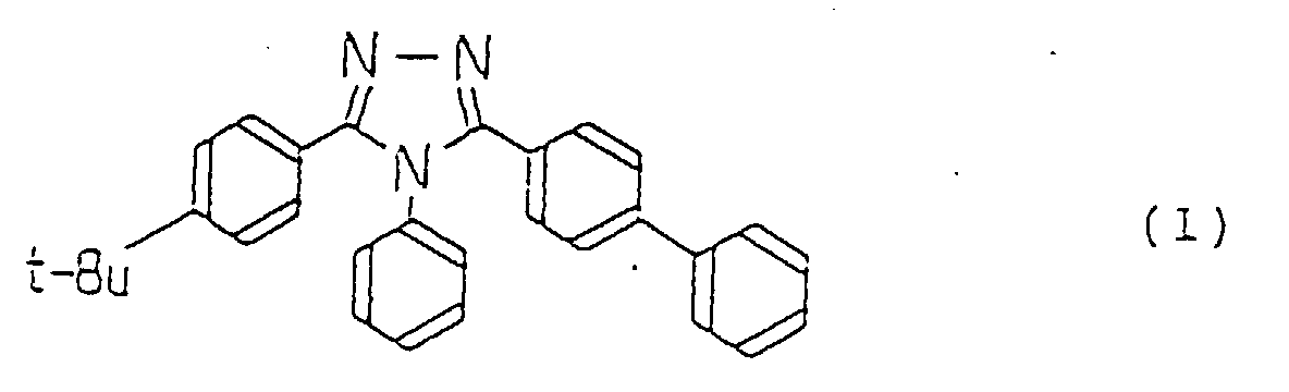
- TAZ 3-(4-biphenylyl)-4-phenyl-5-(4-tert-butylphenyl)-1,2,4-triazole
- the second organic electroluminescent element of the present invention is characterized by a carrier-transport control layer for selectively transporting holes or electrons, which is interposed between a hole-transport layer and an electron-transport layer, wherein the carrier-transport control layer is a layer of TAZ.
- the exciton containment effect due to a carrier-transport control layer composed of TAZ, which selectively transports holes or electrons, provide the hole-transport layer or the electron-transport layer with high luminance and high luminous efficiency as a luminescent layer. It is therefore possible to increase luminous efficiency and luminance as well as stability accompanied thereby.
- a hole-transport layer composed of material capable of emitting blue light emission e.g. the poly-N-vinyl carbazole
- an electron-transport layer promotes luminous efficiency and luminance for blue light emission to a required level for practical applications.
- the carrier-transport control layer by selecting the material and film thickness for the carrier-transport control layer, it is possible to allow the hole-transport layer and/or electron-transport layer to emit light at high luminance and high luminous efficiency. Therefore, one element can emit more than two mutually different emission spectrums, by using different emission spectrum materials for the hole-transport layer and electron-transport layer. This might result in the practical use of light emission such as the multi-color display due to three primary colors of R, G and B, and white light emission.
- the third organic electroluminescent element of the present invention is characterized in that at least one electron-transport layer and at least one hole-transport luminescent layer are provided and that the hole-transport luminescent layer is formed by molecularly dispersing at least one kind of dye in a polymer wherein the electron-transport layer is composed of a single layer of a 1,2,4-triazole derivative, or two layers consisting of the layer of the 1,2,4-triazole derivative and a layer of a tris(8-quinolinolato)aluminum (III) complex expressed by the formula:
- the hole-transport luminescent layer has heat resistance superior to that of a conventional hole-transport layer of a low-molecular material, and is also excellent in adhesion to a substrate such as ITO glass and ITO film. It is therefore possible to form a hole-transport luminescent layer wherein there hardly occurs deterioration, aggregation, crystallization or the like due to heat release when the element emits light, resulting in an increase in stability.
- the combination of the aforesaid hole-transport luminescent layer and an electron-transport layer increases furthermore carrier injection efficiency and the recombination efficiency for holes and electrons, resulting in light emission having high luminous efficiency and high luminance.
- a dye can be easily dispersed in a polymer by adjusting a solution. It is therefore possible to disperse plural dye in one hole-transport luminescent layer. This realizes a multi-color display having good color purity due to three primary color, white light emission and natural light emission, depending upon the dye kind or the dye combination.
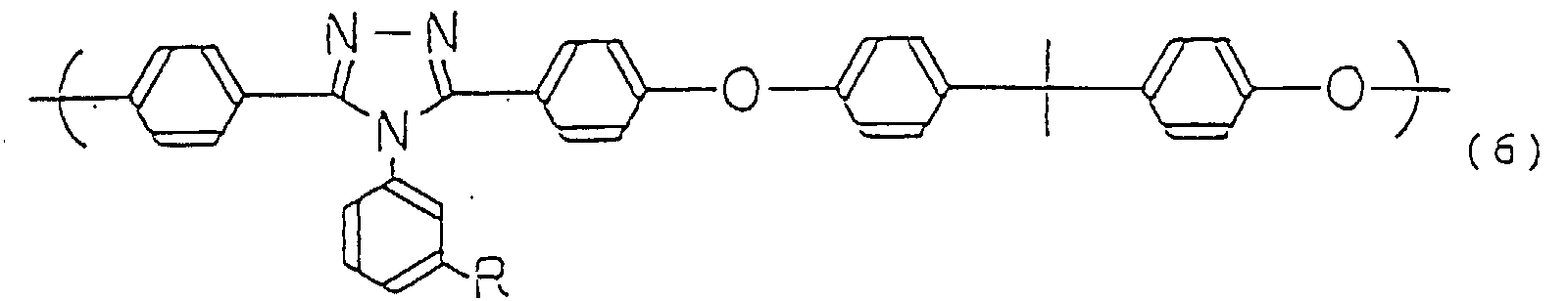
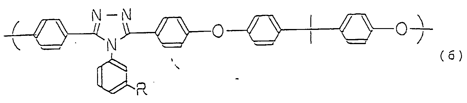
- the fourth organic electroluminescent element of the present invention is characterized in that there is provided with a hole-transport layer which contains, as a hole-transport material, a high-molecular 1,2,4-triazole derivative (hereinafter referred to as "PTAZ") of a repeating unit expressed by the general formula (6): wherein R denotes at least one member selected from the group consisting of a hydrogen atom, a methyl group and an ethyl group.
- PTAZ high-molecular 1,2,4-triazole derivative
- the fifth organic electroluminescent element of the present invention is characterized in that there is provided with a hole-transport layer which contains the PTAZ as a resin binder, and in the hole-transport layer a low-molecular hole-transport material is molecularly dispersed in the PTAZ.
- the PTAZ used in these elements has never been employed as a material for organic electroluminescent elements until the present inventors do so.
- the PTAZ is applicable to a hole-transport material, and yet it is a polymer. Accordingly, it has heat-resistance superior to that of a conventional low-molecular hole-transport material. It is therefore possible to form a hole-transport layer wherein there hardly occurs deterioration, crystallization due to heat release when the element emits light.
- the PTAZ has a higher glass transition temperature (about 200°C or more) than a normal polymer such as polycarbonate, and is excellent in optical characteristics. Therefore, if employed it as a resin binder for a so-called molecular-dispersion hole-transport layer wherein a low-molecular hole-transport material is molecularly dispersed in a resin binder, it is possible to prevent such a hole-transport material from causing aggregation or crystallization due to the aforesaid heat release.
- the PTAZ is greatly useful in increasing stability, luminous efficiency and luminance for an element.
- the PTAZ prevents a luminescent material being excited by the recombination of carriers from forming exciplex together with the hole-transport material.
- the luminescent material emits light at high efficiency, thus increasing luminous efficiency of the element.
- the combination of the PTAZ and a conventional luminescent material for blue light emission whose luminous efficiency is low can raise the luminous efficiency to a required level for practical applications.
- the first to fifth organic electroluminescent elements of the present invention can emit color light as previously mentioned, particularly blue one. Further, these organic electroluminescent elements can emit light of more than two mutually different emission spectrums, and can emit color light such as a multi-color display due to three primary colors and white light emission, which has never been produced with sufficient efficiency or has been failed to emit it at high luminous efficiency.
- Fig. 1(a) is a vertical sectional view illustrating a preferred embodiment of the fist organic electroluminescent element of the present invention
- Fig. 1(b) is a vertical sectional view illustrating one embodiment of the second organic electroluminescent element of the present invention.
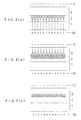
- Figs. 2(a) to 2(c) are schematic diagrams illustrating the principle of light emission of an element wherein the film thickness of the TAZ layer as a carrier-transport control layer is sufficiently large, among the three-layer structure of the second organic electroluminescent element.
- Fig. 3(a) to 3(c) are schematic diagrams illustrating the principle of light emission of an element wherein the film thickness of the TAZ layer as the carrier-transport control layer is sufficiently small.
- Fig. 4(a) to 4(c) are schematic diagrams illustrating the principle of light emission of an element wherein the film thickness of the TAZ layer as a carrier-transport control layer is intermediate between those of Figs. 2 and 3 .
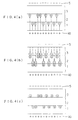
- Fig. 5(a) to 5(c) are schematic diagrams illustrating the principle of light emission of an element having a two-layer structure wherein no TAZ layer is interposed between the TPD layer as a hole-transport layer and the Alq layer as an electron-transport layer.
- Fig. 6(a) is a vertical sectional view illustrating an element whose electron-transport layer has a two-layer structure, among the third organic electroluminescent element
- Fig. 6(b) is a vertical sectional view illustrating an element whose electron-transport layer is a single layer.
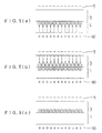
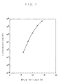
- Fig. 7 is a graph illustrating the measurement results of the relation between drive voltage and luminance in the first organic electroluminescent element prepared in Example 1.
- Fig. 8 is a graph illustrating the measurement results of the relation between drive voltage and luminance in the first organic electroluminescent element prepared in Example 2.
- Fig. 9 is a graph illustrating the measurement results of an emission spectrum of the organic electroluminescent element prepared in Example 2.
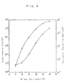
- Fig. 10 is a graph illustrating the measurement results of the relation between drive voltage and luminance in the second organic electroluminescent element prepared in Example 4.
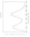
- Fig. 11 is a graph illustrating the measurement results of emission spectrums of the second organic electroluminescent element prepared in Examples 4, 5 and 6.
- Fig. 12 is a graph illustrating the measurement results of emission spectrums of the second organic electroluminescent element prepared in Example 8.
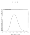
- Fig. 13 is a graph illustrating the measurement results of an emission spectrum of the third organic electroluminescent element prepared in Example 9.
- Fig. 14 is a graph illustrating the measurement results of an emission spectrum of the third organic electroluminescent element prepared in Example 10.
- Fig. 15 is a graph illustrating the measurement results of an emission spectrum of the third organic electroluminescent element prepared in Example 11.
- Fig. 16 is a graph illustrating the measurement results of an emission spectrum of the third organic electroluminescent element prepared in Example 12.
- Fig. 17 is a graph illustrating the measurement results of the relation between drive voltage and luminance in the fifth organic electroluminescent element prepared in Example 16.
- Fig. 18 is a graph illustrating the measurement results of an emission spectrum of the organic electroluminescent element prepared in Example 16.
- Figs. 19(a) to 19(c) are vertical sectional views illustrating the conventional organic electroluminescent elements.
- the following is to describe the first organic electroluminescent element comprising at least one layer of a 1,2,4-triazole derivative.
- a layer of a 1,2,4-triazole derivative used herein denotes a layer containing at least one kind of the low-molecular 1,2,4-triazole derivatives as previously described. There are, for example, a layer which solely comprises one or more kinds of the 1,2,4-triazole derivatives, and a layer wherein one or more kinds of the 1,2,4-triazole derivatives are dispersed in a suitable binder.
- the 1,2,4-triazole derivative layer may contain other ingredients such as various additives, which do not inhibit its function.
- the 1,2,4-triazole derivative layer can be formed by vapor phase deposition such as vacuum deposition, or solution application to apply, on a substrate or the other layer, a solution wherein a material constituting the layer is dissolved in a suitable solvent, followed by drying.
- vapor phase deposition such as vacuum deposition
- solution application to apply, on a substrate or the other layer, a solution wherein a material constituting the layer is dissolved in a suitable solvent, followed by drying.
- TAZ expressed by the formula: because it is excellent in both electron-transport properties and hole-blocking properties.
- the film thickness of this derivative layer is not specifically limited in the present invention. But if it is too thin, hole- block properties become insufficient and, therefore it requires a certain amount of thickness.
- its suitable range is not specifically limited, its lower limit is preferably a range from 100 to 200 ⁇ for a vapor deposited film of the PAZ expressed by the formula (1), in order to hold a sufficient hole-blocking properties.
- the upper limit is not specifically limited, if this layer is too thick, electron-transport properties decreases. For example, it is desired to be not more than 1000 ⁇ for the vapor deposited film of the TAZ.
- the 1,2,4-triazole derivative layer is essential to the first organic electroluminescent element. There are no other construction restrictions. That is, it may be either a conventional single-layer structure or a multi-layer structure. In short, the construction of the first element is applicable to any layers irrespective of the construction kind.
- each layer can be formed by the aforesaid solution application and vapor phase deposition as in the 1,2,4-triazole derivative layer.
- Each layer may contain other ingredients such as resin binders and various additives, which do not directly affect the function of the layer.
- the layer of the 1,2,4-triazole derivative presents excellent electron-transport properties and hole-blocking properties as described above, it is possible to emit blue light emission at high luminance, which has been difficult to realize, by the combination of the 1,2,4-triazole derivative layer as an electron-transport layer and the hole-transport luminescent layer for blue light emission, which has high hole-transport properties.
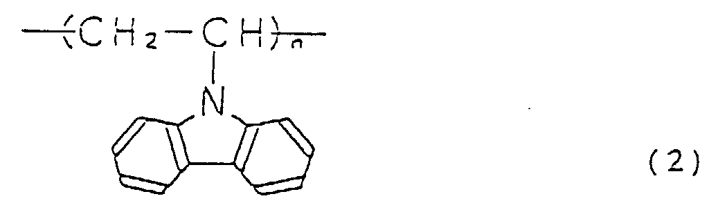
- Most preferred hole-transport luminescent layer for blue light is a layer of poly-N-vinylcarbazole (hereinafter referred to as "PVK”) expressed by the formula: wherein n is the polymerization degree.
- PVK poly-N-vinylcarbazole
- the PVK layer has high hole mobility and, therefore holes injected into the layer escape into a cathode, thus normally failing to emit light.
- the blue light emission can be obtained by combing the PVK layer with the 1,2,4-triazole derivative layer which is excellent in the excitons containment and high hole-blocking properties.
- the PVK also performs the function of the hole-transport material as seen from its molecular structure, and has heat resistance superior to the conventional hole-transport materials such as the low-molecular aromatic tertiary amine compounds as previously described, because it is a polymer. Therefore, it is possible to form a hole-transport luminescent layer for blue light emission wherein there hardly occurs deterioration or crystallization due to heat release on storage or light emission of the element.
- the PVK layer is excellent in adhesion to substrates such as ITO glass and ITO film.
- the combination of the PVK layer as a hole-transport luminescent layer and the 1,2,4-triazole derivative layer realizes an organic electroluminescent element for blue light emission that presents excellent luminous efficiency, luminance and stability and that can be put to practical use.
- the polymerization degree n of the PVK is not specifically limited in the present invention, but it is preferably about 20 to 5000. If it is below this range, heat resistance and adhesion tend to be insufficient. On the other hand, if it is beyond this range, the layer formation by solution application might be difficult.
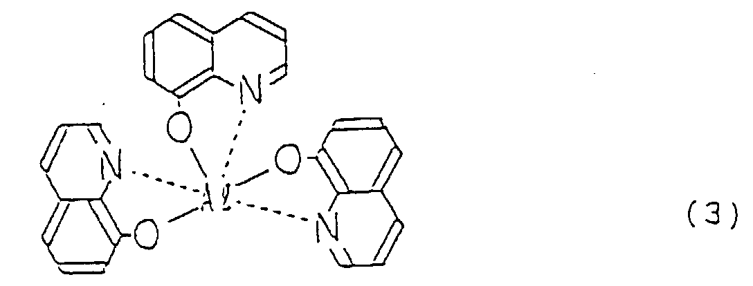
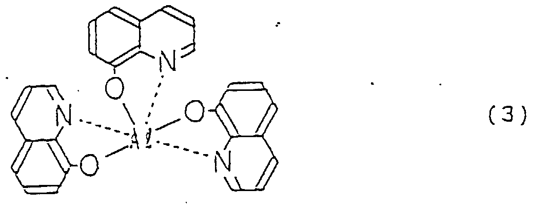
- More preferred element of the combination of the 1,2,4-triazole derivative layer and the PVK layer is that having a three-layer structure wherein a layer of a tris(8-quinolinolato)aluminum (III) complex (hereinafter referred to as "Alq") expressed by the formula: is provided as an electron-transport layer.
- Alq a tris(8-quinolinolato)aluminum (III) complex
- the layer construction of the three-layer structure element is not specifically limited. But, if consideration is given to the fact that the PVK layer is excellent in adhesion to substrates such as ITO glass and ITO film, and is formed exclusively by solution application, it is preferable to use an element wherein three layers: a hole-transport luminescent layer (a PVK layer) 10 , a layer of a 1,2,4-triazole derivative (a TAZ layer) 20 and an electron-transport layer (an Alq layer) 30 are laminated in this order on an anode 40 of a transparent conductive material such as ITO (indium-tin-oxide) being formed on a glass substrate 4 , as shown in Fig. 1(a) .
- the reference numerals 5 and B denote a cathode of metal deposited film such as Mg/Ag and a power source for applying a drive voltage to the element, respectively.
- the film thickness for the PVK layer 10 and the Alq layer 30 is not specifically limited in the present invention. They can be set to an appropriate range depending upon the kind of the 1,2,4-derivative to be used and the film thickness of the layers.
- the PVK layer 10 can be formed by the aforesaid solution application.
- the Alq layer 30 contains at least the Alq.
- the Alq layer 30 can be formed by the aforesaid solution application and vapor phase deposition.
- the PVK layer 10 and the Alq layer 30 may contain other ingredients such as various additives, which do not inhibit the functions of the PVK and the Alq.
- the followings is to describe the second organic electroluminescent element having a three-layer structure comprising a carrier-transport control layer, which is interposed between a hole-transport layer and an electron-transport layer.
- This element is, as shown in Fig. 1(b) , composed of laminated three layers: a hole-transport layer 1 ; a carrier-transport control layer 2 and an electron-transport layer 3 , which are formed in this order or in the reverse order, on an anode 40 of a transparent conductive material such as ITO (indium-tin-oxide) being formed on a glass substrate 4 . It is essential that the layer 2 is sandwiched between the layers 1 and 3 .
- reference numerals 5 and B denote a cathode of metal deposited film such as Mg/Ag and a power source for applying a drive voltage to the element, respectively, likewise in Fig. 1(a) .
- carrier-transport control material for the carrier-transport control layer 2 TAZ is used.
- the carrier-transport control layer 2 functions such that either or both of the hole-transport layer 1 or/and electron-transport layer 3 emit light at high luminance and high efficiency depending upon its material and its film thickness as previously described.
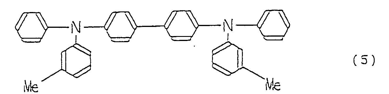
- the function of the carrier-transport control layer 2 will be described through an example which employs a vapor deposited film of the TAZ (the TAZ layer) as a carrier-transport control layer 2 , a vapor deposited layer of a N,N'-diphenyl-N,N'-bis(3-methylphenyl)-1,1'-biphenyl-4,4-diamine (hereinafter referred to as "TPD") expressed by the formula: (the TPD layer) as a hole-transport layer 1 and a vapor deposited film of the Alq (the Alq layer) expressed by the formula (3) as an electron-transport luminescence layer 3 .
- TPD N,N'-diphenyl-N,N'-bis(3-methylphenyl)-1,1'-biphenyl-4,4-diamine
- carrier injection into an organic insulating film is restricted by space charge.
- the current capacity that passes through the organic insulating film is proportional to the mobility of carriers and the square of the electric field strength, and is inversely proportional to the cubic of the film thickness of the organic insulating film. That is, the larger the electric field strength and mobility, the more carrier injection is accelerated. The larger the film thickness, the more carrier injection is restricted.
- the electric field strength applied on the Alq layer 3 becomes larger than the apparent electric field strength applied between a couple of electrodes 40 , 5 because of the space charge on the TPD/Alq interface, thereby initiating an electron injection into the Alq layer 3 (Fig. 5(b) ).
- the injection order for holes and electrons are the same.
- the film thickness of the TAZ layer 2 is sufficiently large (for example, about 150 ⁇ or more) as shown in Fig. 2 , the TAZ layer 2 exhibits excellent hole-blocking properties similar to the first element, so that holes thus injected are blocked at the TPD/TAZ interface (Fig. 2(a) ).
- Electrons which are being injected into the Alq layer 3 by the formation of the space charge due to the holes are transported to the TPD/TAZ interface because the TAZ layer 2 is excellent in electron-transport properties (Fig. 2(b) ), and excitons are generated by the recombination of the holes and the electrons (Fig. 2(c) ) and the TPD whose excitation energy level is lower than that of the TAZ is excited by the excitons thus generated to emit light.
- the film thickness of the TAZ layer 2 is sufficiently small (for example, about 50 ⁇ or less), as shown in Fig. 3 , holes injected into the TPD layer 1 by applying a bias voltage between a couple of electrodes 40 , 5 pass through the TAZ layer 2 and are blocked at the TAZ/Alq interface to form space charge (Fig. 3(a) ).
- the reason why the holes pass through the TAZ layer 2 is that the injection amount of carriers (the holes in this case) is inversely proportional to the cubic of the film thickness of the TAZ layer 2 being the organic insulating film.
- the film thickness of the TAZ layer 2 is intermediate between the above value (in case of being in a range from about 50 to about 150 ⁇ )
- some of the holes which are injected into the TPD layer 1 by applying a bias voltage between a couple of electrodes 40 , 5 are blocked on the TPD/TAZ interface, the others pass through the TAZ layer 2 and are blocked on the TAZ/Alq interface (Fig. 4(a) ).
- the injection amount of the holes is inversely proportional to the cubic of the film thickness of the TAZ layer 2 , as described above.
- the TAZ layer of the element in Fig. 4 allows both of the holes and the electrons to pass through, the recombination of both may occur in the TAZ layer 2 .
- the TAZ has a peak light emission at a shorter wavelength region of not more than 4000 nm. Even if the TAZ is excited by the excitons generated by the above recombination, excitation energy is transported to either or both of the TPD layer or/and the Alq layer, each having a peak light emission at a longer wavelength region. Consequently, the TAZ layer 2 itself emits no light.
- the function of the TAZ layer can be changed by adjusting its film thickness within the above range, in the combination of the TPD layer 1 , the TAZ layer 2 and the Alq layer 3 .
- the relation between the functions of the carrier-transport control layer 2 and its film thickness may not necessarily correspond with the above examples.
- the range of the film thickness of the layer 2 having a specific function varies depending upon factors such as material constituting the respective layers, the layer structure (e.g. a vapor deposited film, a binder dispersed film, etc.).
- the combination of the hole-transport layer 1 and electron-transport layer 3 which emit light at different spectrums likewise in the combination of the TPD layer and the Alq layer also offers the advantage that the color tone of the overall emission color being a mixed color of both layers' emission colors can be finely adjusted by suitably selecting the film thickness of the carrier-transport control layer 2 .
- a hole-transport layer 1 In the second element, it is essential to have three layers: a hole-transport layer 1 ; a carrier-transport control layer 2 and an electron-transport layer 3 . No particular restrictions are imposed upon other constructions.
- the carrier-transport control layer 2 may be solely composed of TAZ as the carrier-transport control material, or may be formed by dispersing it in a suitable binder.
- the carrier-transport control layer 2 may contain other ingredients such as various additives, which do not inhibit its function.
- the respective layers including the carrier-transport control layer 2 can be formed by the aforesaid solution application or vapor phase deposition.
- the following is to describe the third organic electroluminescent element wherein a hole-transport luminescent layer is formed by molecularly dispersing at least one kind of dye in a polymer.
- the polymer constituting the hole-transport luminescent layer may or may not have carrier-transport properties.
- the polymer having no carrier-transport properties there may provide it with hole-transport properties by molecularly dispersing a low-molecular hole-transport material along with a dye.
- polystyrene resin examples include polyphenylenevinylene and its derivative, polyalkylthiophene, the PVK, polymethylphenylsilane, polymer having a triphenylamine group at a side chain or main chain, among others. Most preferred is the PVK because its carrier-transport properties are stable.
- the polymerization degree n of the PVK is preferably about 20 to 5000 for the same reason above-mentioned.
- polymers having excellent optical characteristics can be employed.
- these are polymethyl methacrylate, polycarbonate, polystyrene, polysulfon, polyether sulfon, polyallylate.
- the dye to be molecularly dispersed in the polymer may be one of the aforesaid dyes for laser, which can be excited by excitons to generate fluorescence.
- these dyes include cyanine dye, xanthene dye, oxazine dye, coumarin derivative, perylene derivative, acridine dye, acridone dye, quinoline dye, among others.
- TPB blue light emission
- DCM 4-dicyanomethylene-2-methyl-6-p-dimethylaminostyryl-4H-pyran
- the combination of the TPB of the formula (7), the coumarine 6 of the formula (8) and the DCM of the formula (10) is appropriate. This combination allows the emission spectrum of the hole-transport luminescent layer to extend over the whole visible light region having a wavelength of 400 to 700 nm, resulting in a good white light emission.
- the proportion of the dye formulated in a polymer is not specifically limited, and a preferable range can be set depending upon the kinds of polymer and dye, luminescence intensity, color tone and the like.
- a triphenylamine derivative as a lower molecular hole-transport material to be molecularly dispersed in the polymer. More preferred is the TPD.
- the hole-transport luminescent layer comprising the above respective components can be formed by the aforesaid solution application.
- an electron-transport layer used in the combination with the hole-transport luminescent layer there is employed a single layer of a 1,2,4-triazole derivative, or a two-layer structure layer wherein the layer of the 1,2,4-triazole derivative and the Alq layer are laminated with each other.
- the 1,2,4-triazole derivative is excellent both in electron-transport properties and hole-blocking properties, the recombination of electrons and holes can be sufficiently conducted in the hole-transport luminescent layer and, at the same time, generated excitons can be efficiently contained in the hole-transport luminescent layer, resulting in a further increase in luminous efficiency and luminance of the hole-transport luminescent layer.
- a suitable example of the low-molecular 1,2,4-triazole derivative is the TAZ which is excellent in both electron- transport properties and hole-blocking properties.
- the film thickness of the 1,2,4-triazole derivative layer is not specifically limited, if it is too thin, hole-blocking properties becomes insufficient. Thus it is desirable to have an ample film thickness. Although its suitable range is not specifically limited, 100 to 200 ⁇ or more is appropriate for the vapor deposited film of the TAZ expressed by the formula (1) in order to hold a sufficient hole-blocking properties. The upper limit of its film thickness is not specifically limited, but electron-transport properties would decrease if it is too thick. Therefore, for the vapor deposited film of the TAZ, its film thickness is preferably not more than 1000 ⁇ .
- the film thickness of the Alq layer is not specifically limited, but its film thickness is preferably about 100 to 1000 ⁇ , considering the electron injection properties and the electron-transport properties to the hole-transport luminescent layer. If the Alq layer is laminated, it can be complementary to the hole-blocking properties of the 1,2,4-triazole derivative layer. Therefore, the film thickness of the 1,2,4-triazole derivative layer may be smaller than the aforesaid range for the vapor deposited film of the TAZ.
- the total film thickness of both layers is not specifically limited, it is preferably about 200 to 1500 ⁇ . If it is smaller than this range, hole-block properties tends to be insufficient. On the other hand, if it is larger than that, electron-transport properties tends to decrease.
- the electron-transport layer such as the 1,2,4-triazole derivative layer and the Alq layer may be solely composed by an electron-transport material such as the 1,2,4-triazole derivative and the Alq, or be formed by dispersing an electron-transport material in a suitable binder.
- the electron-transport layer may contain other ingredients such as various additives which do not inhibit its function.
- the electron-transport layer can be formed by the aforesaid solution application or vapor phase deposition.
- the layer construction of the third element is not specifically limited.
- the polymer constituting the hole-transport luminescent layer is excellent in adhesion to substrates such as the ITO glass and the ITO film, and is formed exclusively by the solution application , it is preferable to use those prepared by laminating two layers: a hole-transport luminescent layer 11 and an electron-transport layer 31 on an anode 40 of a transparent conductive material such as ITO (indium-tin-oxide) being formed on a glass substrate 4 in this order, as shown in Figs. 6(a) and 6(b) .
- a transparent conductive material such as ITO (indium-tin-oxide)
- the electron-transport layer 31 of Fig. 6(a) has a two-layer structure wherein two layers of the 1,2,4-triazole derivative layer (the TAZ layer) 31a and the Alq layer 31b are laminated on a hole-transport luminescent layer 11 in this order.
- the reference numerals 5 and B denote a cathode of metal deposited film such as Mg/Ag and Al/Li and a power source for applying a drive voltage to the element, respectively.
- the followings is to describe the fourth organic electroluminescent element comprising a hole-transport layer which contains the PTAZ as a hole-transport material, and the fifth organic electroluminescent element comprising a hole-transport layer which contains the PTAZ as a resin binder in the present invention.
- PTAZ-1 those having a repeating unit expressed by the formula:
- PTAZ-2 those having a repeating unit expressed by the formula:
- the polymerization degree of the PTAZ is not specifically limited in the present invention, but it is preferably about 3000 to about 30000. If it is below this range, heat resistance tends to be insufficient. On the other hand, if it is beyond this range, the layer formation by the solution application might become difficult.
- one or more kinds of the PTAZ are used as a hole-transport material to form a hole-transport layer primarily composed of the PTAZ.
- one or more kinds of the PTAZ are used, as a resin binder, and a low-molecular hole-transport material is molecularly dispersed in the resin binder to form a hole-transport layer.
- the TPD is suitable for the low-molecular hole-transport material.
- Both hole-transport layers may contain other ingredients such as various additives which do not inhibit the function of the PTAZ and the TPD.
- the film thickness of the hole-transport layer is not specifically limited in the present invention, and it can be set to the optimum range depending upon the structure characteristics, namely, to which type it belongs.
- the hole-transport layer can be formed by the aforesaid solution application.
- both elements it is essential to have a hole-transport layer containing the PTAZ. No other particular restrictions are imposed thereon. They can employ either a conventional two-layer structure or a multi-layer structure comprising three or more layers. In short, the construction of both elements are applicable to any elements of various layer structures.
- the layer material other than the hole-transport layer, which constitutes the element of the two-layer structure or the multi-layer structure, is not specifically limited in the present invention.
- Various conventional materials may be used for the respective layers.
- the film thickness of the respective layers constituting the element is not specifically limited in the present invention.
- the respective layers can be formed by the aforesaid solution application and vapor phase deposition, likewise in the hole-transport layer.
- Each layer may contain other ingredients such as resin binders and various additives which are not directly related to the layers' functions.
- a protective layer may be coated to shield the element against transmission of water or oxygen in air, or an element coated with the protective layer may be further sealed with a glass or a polymer, in order to improve storage stability in air or to extend the lifetime at the time of a continuous light emission.
- every organic electroluminescent element of the present invention drives at a lower voltage, and is valid for producing a large-area luminescent element having flexibility because it is composed of organic material.
- a great applicability in the fields of indication, illumination and display is a great applicability in the fields of indication, illumination and display.
- the TPD expressed by the formula (5) as a hole-transport material, the Alq expressed by the formula (3) as an electron-transport material and the TAZ expressed by the formula (1) as a 1,2,4-triazole derivative were deposited in this order by vacuum deposition to form a TPD layer, an Alq layer and a TAZ layer, respectively.
- the luminescent region was expressed by a square being 0.5 cm in side. The deposition conditions for each layer:
- the deposition rate of the electrode layer was 11 ⁇ /sec. and that of the protective layer was 10 ⁇ /sec.
- the ITO film and the Mg/Ag electrode layer thus prepared were used as an anode and a cathode, respectively, and a bias voltage was applied between a couple of electrodes at room temperature in air to allow the luminescent layer to emit light. Its luminance was measured using a luminance meter (Model No. LS-100, available from Minolta Co., Ltd.).
- the PVK expressed by the formula (2) as a hole-transport luminescent material was coated by a dip coating using dichloroethane as a solvent to form a PVK layer, on which the TAZ expressed by the formula (1) as a 1,2,4-triazole derivative and the Alq expressed by the formula (3) as an electron-transport material were deposited in this order by vacuum deposition to form a TAZ layer and an Alq layer, respectively.
- the luminescent region was expressed by a square being 0.5 cm in side.
- the deposition conditions were the same as in Example 1.
- Each film thickness was:
- the deposition rates for the electrode layer and protective layer were the same as in Example 1.
- the ITO film and the Mg/Ag electrode layer of the organic electroluminescence thus prepared were used as an anode and a cathode, respectively, and a bias voltage was applied between a couple of electrodes at room temperature in air to allow the luminescent layer to emit light. Its luminance was measured using the aforesaid luminance meter.
- the blue light emission was measured at room temperature using a fluorophotometer (Model No. F4010 available from Hitachi Co, Ltd.).
- Example 2 In the same manner as in Example 2 except that the Alq layer was omitted, an organic electroluminescent element was prepared and its characteristics were examined.
- a voltage for initiating light emission became slightly large and a maximum current became small, but there obtained blue light emission with high luminance similar to Example 2.
- Example 2 In the same manner as in Example 2 except that the TAZ layer was omitted, an organic electroluminescent element was prepared and its characteristics were examined.
- This element exhibited green light emission whose peak is at a wavelength of 530 nm. This emission color proved that the light emission originated from the Alq layer, not the PVK layer. This finding showed that the combination of the PVK layer and the TAZ layer is essential to allow the PVK layer to emit blue light.
- An organic electroluminescent element composed of the PVK layer alone was prepared wherein the TAZ layer and the Alq layer were omitted.
- the luminance of light emission was too weak to evaluate its luminance.
- the TPD, the TAD and the Alq were deposited in this order by vacuum deposition to form a TPD layer, a TAD layer and an Alq layer, respectively.
- the luminescent region was expressed by a square being 0.5 cm in side.
- the deposition conditions were the same as in Example 1.
- Each film thickness was as follows:
- the deposition rates for the electrode layer and the protective layer were the same as in Example 1.
- the ITO film and the Mg/Ag electrode layer thus prepared were used as an anode and a cathode, respectively, and a bias voltage was applied between a couple of electrodes at room temperature in air to allow the luminescent layer to emit light. Its luminance was measured using the aforesaid luminance meter.
- the blue light emission was measured at room temperature using the aforesaid fluorophotometer. There observed an emission spectrum having a peak at a wavelength of 464 nm, as shown by a solid line in Fig. 11 . The emission spectrum nearly corresponded to the emission spectrum of the vapor deposited film composed of the TPD alone, shown by a short broken line in Fig. 11 . This proved that the light emission originated from the TPD layer of Example 4.
- Example 5 There employed an organic electroluminescent element having the same layer structure as in Example 4, but the film thickness of the TAZ layer as a carrier-transport control layer was changed to 50 ⁇ (Example 5) or 100 ⁇ (Example 6) to measure each emission spectrum in the same manner as in Example 4.
- Example 5 exhibited a green emission spectrum being luminescent color of the Alq layer, as shown by a chain line in Fig. 11 .
- Example 6 such a green light emission became remarkably small and, at the same time, blue light emission being the emission color of the TPD layer became large, as shown by a long broken line in Fig. 11, resulting in blue-green light emission of both color emissions being mixed.
- Example 8 In the same manner as in Example 4, in the element whose TAZ layer had a film thickness of 300 ⁇ (Example 8), as shown in Fig. 12, there observed light emission of blue-green wherein green light emission being the luminescent color of the Alq layer was mixed with blue light emission being the luminescent color of the TPD layer.
- the PVK expressed by the formula (2), 5 molar % (for PVK) of the TPB expressed by the formula (7), 0.3 molar % (for PVK) of coumarine 6 expressed by the formula (8) and 0.3 molar % (for PVK) of the DCM expressed by the formula (10) were dissolved in dichloromethane to prepare an application solution.
- the application solution was applied on an ITO (indium-tin-oxide) coated glass substrate having a sheet resistance of 15 ⁇ / ⁇ (ITO film thickness: 1500 to 1600 ⁇ , manufactured by Asahi Glass Co., Ltd.) by dip coating, followed by drying to form a hole-transport luminescent layer.
- the TAZ expressed by the formula (1) and the Alq expressed by the formula (3) as an electron-transport material were deposited in this order by vacuum deposition to form an electron-transport layer of a two-layer structure.
- the luminescent region was expressed by a square being 0.5 cm in side.
- the deposition conditions for the TAZ layer and Alq layer were as follows:
- the deposition rate for the electrode layer and that of the protective layer were 11 ⁇ /sec. and 10 ⁇ /sec., respectively.
- the ITO film and the Mg/Ag electrode layer thus prepared were employed as an anode and a cathode, respectively, and a bias voltage was applied between a couple of electrodes at room temperature in air to allow the luminescent layer to emit light. Its luminance was measured using the aforesaid luminance meter.
- the white light emission was measured at room temperature using the aforesaid fluorophotometer. There obtained an emission spectrum that extended over a range of visible light having a wavelength of 400-700 nm, as shown in Fig. 13 .
- Example 9 In the same manner as in Example 9 except that an application solution was prepared by dissolving the PVK and 5 molar % (for PVK) of the TPB in dichloromethane, an organic electroluminescent element was prepared and its characteristics were examined.
- the blue light emission was measured using the aforesaid fluorophotometer. There obtained an emission spectrum having a peak at a wavelength of 450 nm, as shown in Fig. 14 . This proved that blue light emission originated from the TPB.
- Example 9 In the same manner as in Example 9 except that an application solution was prepared by dissolving the PVK and 1 molar % (for PVK) of the coumarine 6 in dichloromethane, an organic electroluminescent element was prepared and its characteristics was examined.
- Example 9 In the same manner as in Example 9 except that an application solution was prepared by dissolving the PVK and 0.1 molar % (for PVK) of the DCM in dichloromethane, an organic electroluminescent element was prepared and its characteristics was examined.
- the white light emission was measured using the aforesaid fluorophotometer. As a result, it was confirmed that the white light emission originated from the light emission of the PVK whose wavelength is 410 nm and light emission of the DCM whose wavelength is 550 nm.
- the PTAZ-1 expressed by the formula (6a) as a hole-transport material was coated by dip coating using dichloromethane as a solvent to form a PTAZ-1 layer.
- the Alq expressed by the formula (3) as an electron-transport material was applied vacuum deposition the PTAZ-1 layer to form a Alq layer.
- the luminescent region was represented by a square being 0.5 cm in side.
- the deposition conditions were:
- the deposition rate for the electrode layer and the protective layer were 11 ⁇ /sec. and 10 ⁇ /sec., respectively.
- the ITO film and the Mg/Ag electrode layer thus prepared were used as an anode and a cathode, respectively, and a bias voltage was applied between a couple of electrodes at room temperature in air to allow the luminescent layer to emit light. Its luminance was measured using the aforesaid luminance meter. Light emission of 1200 cd/m 2 in luminance at a drive voltage of a maximum 16 V (180mA/cm 2 ) was observed.
- Example 13 In the same manner as in Example 13 except that the PTAZ-2 expressed by the formula (6b) as a material of constituting a hole-transport layer was used in place of the PTAZ-1, an organic electroluminescent was prepared and its luminance was measured.
- the deposition rates for the electrode layer and the protective layer were the same as in Example 13.
- the ITO film and the Mg/Ag electrode layer thus prepared were used as an anode and a cathode, respectively, and a bias voltage was applied between a couple of electrodes at room temperature in air to allow the luminescent layer to emit light. Its luminance was measured using the aforesaid luminance meter.
- Example 15 In the same manner as in Example 15 except that a hole-transport layer composed of the TPD alone was formed by vacuum deposition in place of the PTAZ-2:TPD layer, an organic electroluminescent element was prepared [a TPD layer (a hole-transport layer): 500 ⁇ , an Alq layer (an electron-transport layer): 500 ⁇ ], and its luminance was measured in the aforesaid manner.
- the element was preserved at room temperature for several days. As a result, it was confirmed that black points occurred on the luminescent surface and that the TPD was crystallized.
- a PTAZ-2 wherein 30 % by weight of the TPD was molecularly dispersed was coated by dip coating using dichloromethane as a solvent to form a PTAZ-2:TPD layer, on which a 2,5-bis(5-tert-butyl-2-benzooxazolyl)-thiophene (hereinafter referred to as "BBOT") expressed by the formula: as a luminescent material and the TAZ expressed by the formula (1) as an electron-transport material were deposited in this order by vacuum deposition method to form a BBOT layer and a TAZ layer.
- the luminescent region was represented by a square being 0.5 cm in side.
- the deposition conditions were the same as in Example 13.
- Each film thickness was:
- the deposition rates for the electrode layer and protective layer were the same as in Example 13.
- the ITO film and the Mg/Ag electrode layer of the organic electroluminescence thus prepared were used as an anode and a cathode, respectively, and a bias voltage was applied between a couple of electrodes at room temperature in air. As a result, blue light emission with good efficiency was obtained.
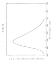
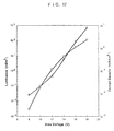
- the luminance was measured in the same manner as in Examples 13 to 15. There observed light emission of 100 cd/m 2 in luminance at a drive voltage of a maximum 18 V (8 mA/cm 2 ), as shown in Fig. 17 (wherein a plot ⁇ - ⁇ denotes the relation between an applied voltage and luminance, and another plot ⁇ - ⁇ denotes the relation between an applied voltage and a current density).
- the light emission was measured at room temperature using the aforesaid fluorophotometer.
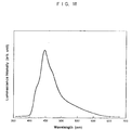
- An emission spectrum was obtained having a peak at a wavelength of 443 nm, as shown in Fig. 18 .
- the emission spectrum corresponded to that of the BBOT. This proved that light emission originated from the BBOT layer of Example 16.
- Example 16 In the same manner as in Example 16 except that a hole-transport layer composed of the TPD alone was prepared by vacuum deposition in place of the PTAZ-2:TPD layer, thus obtaining an organic electroluminescent element comprising a TPD layer (a hole-transport layer): 400 ⁇ ; a BBOT layer (a luminescent layer): 700 ⁇ and a TAZ layer (an electron-transport layer): 400 ⁇ .
- This element emitted light with poor luminance efficiency.
Claims (16)
- Organisches Elektrolumineszenzelement, umfassend mindestens eine Schicht eines 1,2,4-Triazolderivats.
- Organisches Elektrolumineszenzelement nach Anspruch 1, wobei das 1,2,4-Triazolderivat 3-(4-Biphenylyl)-4-phenyl-5-(4-tert-butylphenyl)-1,2,4-triazol ist, ausgedrückt durch die Formel:
- Organisches Elektrolumineszenzelement nach Anspruch 1, welches als eine Lochtransport-Lumineszenzschicht eine Schicht von Poly-N-vinylcarbazol umfaßt, ausgedrückt durch die Formel:worin n den Polymerisationsgrad angibt.

- Organisches Elektrolumineszenzelement nach Anspruch 3, welches als eine Elektronentransportschicht eine Schicht aus einem Tris(8-chinolinolato)aluminium(lll)-Komplex der Formelumfaßt.
- Elektrolumineszenzelement nach Anspruch 1, umfassend eine Träger-Transport-Kontrollschicht zum selektiven Transportieren von Löchern und/oder Elektronen, welche zwischen einer Lochtransportschicht und einer Elektronentransportschicht angeordnet ist, wobei die Träger-Transport-Kontrollschicht eine Schicht von 3-(4-Biphenylyl)-4-phenyl-5-(4-tert-butylphenyl)-1,2,4-triazol, ausgedrückt durch die Formel:ist.

- Organisches Elektrolumineszenzelement nach Anspruch 5, wobei die Lochtransportschicht eine Schicht aus N,N'-Diphenyl-N, N'-bis(3-methylphenyl)-1,1'-biphenyl-4,4-diamin ist, ausgedrückt durch die Formelund die Elektronentransportschicht eine Schicht aus einem Tris(8-chinolinolato)aluminium(III)-Komplex der Formel
 ist.
ist.
- Organisches Elektrolumineszenzelement nach Anspruch 1, umfassend mindestens eine Elektronentransportschicht und mindestens eine Lochtransportlumineszenz-Schicht, wobei die Lochtransportlumineszenzschicht aus einem Polymer und mindestens einer Sorte eines Farbstoffs aufgebaut ist, welcher in dem Polymer molekular dispergiert ist, wobei die Elektronentransportschicht aus einer einzelnen Schicht eines 1,2,4-Triazolderivats oder aus zwei Schichten, bestehend aus der Schicht des 1,2,4-Triazolderivats und einer Schicht eines Tris(8-chinolinolato)aluminium (III)-Komplexes, ausgedrückt durch die Formelaufgebaut ist.
- Organisches Elektrolumineszenzelement nach Anspruch 7, wobei das 1,2,4-Triazolderivat 3-(4-Biphenylyl)-4-phenyl-5-(4-tert-butylphenyl)-1,2,4-triazol ist, ausgedrückt durch die Formel:
- Organisches Elektrolumineszenzelement nach Anspruch 7, wobei die Lochtransportlumineszenschicht aus einem Polymer mit Trägertransporteigenschaften und einem Farbstoff, welcher molekular in dem Polymer dispergiert ist, aufgebaut ist.
- Organisches Elektrolumineszenzelement nach Anspruch 9, wobei das Polymer mit Trägertransporteigenschaften ein Poly-N-vinylcarbazol ist, ausgedrückt durch die Formel:worin n den Polymerisationsgrad angibt.
- Organisches Elektrolumineszenzelement nach Anspruch 7, wobei die Lochtransportlumineszenz-Schicht aus einem Polymer, das keine Trägertransporteigenschaften aufweist, einem Farbstoff und einem niedermolekularen Lochtransportmaterial, die in dem Polymer molekular dispergiert sind, aufgebaut ist.
- Organisches Elektrolumineszenzelement nach Anspruch 11, wobei das niedermolekulare Lochtransportmaterial, das neben dem Farbstoff molekular in dem Polymer, das keine Trägertransporteigenschaften aufweist, dispergiert ist, N,N'-Diphenyl-N,N'-bis(3-methylphenyl)-1,1'-biphenyl-4,4-diamin ist, ausgedrückt durch die Formel

- Organisches Elektrolumineszenzelement nach Anspruch 7, wobei eine Vielzahl von Farbstoffen, die in der Lochtransportlumineszenzschicht molekular dispergiert sind, derart kombiniert sind, daß sich das Emissionsspektrum der Lochtransportlumineszenzschicht über den gesamten Bereich des sichtbaren Lichts mit einer Wellenlänge von 400 bis 700 nm erstreckt.
- Organisches Elektrolumineszenzelement nach Anspruch 1, umfassend eine Lochtransportschicht, welche als Lochtransportmaterial ein höhermolekulares 1,2,4-Triazolderivat einer wiederkehrenden Einheit, ausgedrückt durch die allgemeine Formelenthält, worin R mindestens ein Mitglied, ausgewählt aus der Gruppe, bestehend aus einem Wasserstoffatom, einer Methylgruppe und einer Ethylgruppe, bezeichnet.
- Organisches Elektrolumineszenzelement nach Anspruch 1, umfassend eine Lochtransportschicht, welche durch molekulares Dispergieren eines niedermolekularen Lochtransportmaterials in einem hochmolekularen 1,2,4-Triazolderivat einer wiederkehrenden Einheit, ausgedrückt durch die allgemeine Formel:wobei R mindestens ein Mitglied, ausgewählt aus der Gruppe, bestehend aus einem Wasserstoffatom, einer Methylgruppe und einer Ethylgruppe, als Harzbinder gebildet ist.
- Organisches Elektrolumineszenzelement nach Anspruch 15, wobei das niedermolekulare Lochtransportmaterial, welches in dem 1,2,4-Triazolderivat als Harzbinder molekular dispergiert ist, ein N,N'-Diphenyl-N-N'-bis(3-methylphenyl)-1,1'-bisphenyl-4,4-diamin ist, ausgedrückt durch die Formel:
Applications Claiming Priority (16)
| Application Number | Priority Date | Filing Date | Title |
|---|---|---|---|
| JP6878393 | 1993-03-26 | ||
| JP68783/93 | 1993-03-26 | ||
| JP6878393 | 1993-03-26 | ||
| JP12292793 | 1993-05-25 | ||
| JP122927/93 | 1993-05-25 | ||
| JP12292793 | 1993-05-25 | ||
| JP14784993 | 1993-06-18 | ||
| JP5147849A JP2734338B2 (ja) | 1993-06-18 | 1993-06-18 | 有機エレクトロルミネッセンス素子 |
| JP147849/93 | 1993-06-18 | ||
| JP5186223A JP2734341B2 (ja) | 1993-03-26 | 1993-07-28 | 有機エレクトロルミネッセンス素子 |
| JP18622393 | 1993-07-28 | ||
| JP186224/93 | 1993-07-28 | ||
| JP18622493 | 1993-07-28 | ||
| JP186223/93 | 1993-07-28 | ||
| JP18622493 | 1993-07-28 | ||
| PCT/JP1994/000435 WO1994022974A1 (en) | 1993-03-26 | 1994-03-17 | Organic electroluminescent elements |
Publications (3)
| Publication Number | Publication Date |
|---|---|
| EP0647694A1 EP0647694A1 (de) | 1995-04-12 |
| EP0647694A4 EP0647694A4 (de) | 1995-07-26 |
| EP0647694B1 true EP0647694B1 (de) | 1999-09-15 |
Family
ID=27524137
Family Applications (1)
| Application Number | Title | Priority Date | Filing Date |
|---|---|---|---|
| EP19940910036 Expired - Lifetime EP0647694B1 (de) | 1993-03-26 | 1994-03-17 | Organische elektroluminineszente elementen |
Country Status (5)
| Country | Link |
|---|---|
| US (1) | US5869199A (de) |
| EP (1) | EP0647694B1 (de) |
| DE (1) | DE69420656T2 (de) |
| SG (1) | SG59953A1 (de) |
| WO (1) | WO1994022974A1 (de) |
Cited By (19)
| Publication number | Priority date | Publication date | Assignee | Title |
|---|---|---|---|---|
| EP1298737A2 (de) * | 2001-09-28 | 2003-04-02 | Eastman Kodak Company | Organische Licht emittierende Diode mit einer Zwischenschicht zwischen der Löcher transportierenden Schicht und der Licht emittierenden Schicht |
| US8888318B2 (en) | 2010-06-11 | 2014-11-18 | Intematix Corporation | LED spotlight |
| US8946998B2 (en) | 2010-08-09 | 2015-02-03 | Intematix Corporation | LED-based light emitting systems and devices with color compensation |
| US8947619B2 (en) | 2006-07-06 | 2015-02-03 | Intematix Corporation | Photoluminescence color display comprising quantum dots material and a wavelength selective filter that allows passage of excitation radiation and prevents passage of light generated by photoluminescence materials |
| US8957585B2 (en) | 2010-10-05 | 2015-02-17 | Intermatix Corporation | Solid-state light emitting devices with photoluminescence wavelength conversion |
| US8992051B2 (en) | 2011-10-06 | 2015-03-31 | Intematix Corporation | Solid-state lamps with improved radial emission and thermal performance |
| US8994056B2 (en) | 2012-07-13 | 2015-03-31 | Intematix Corporation | LED-based large area display |
| US9004705B2 (en) | 2011-04-13 | 2015-04-14 | Intematix Corporation | LED-based light sources for light emitting devices and lighting arrangements with photoluminescence wavelength conversion |
| US9045688B2 (en) | 2006-08-03 | 2015-06-02 | Intematix Corporation | LED lighting arrangement including light emitting phosphor |
| US9115868B2 (en) | 2011-10-13 | 2015-08-25 | Intematix Corporation | Wavelength conversion component with improved protective characteristics for remote wavelength conversion |
| US9217543B2 (en) | 2013-01-28 | 2015-12-22 | Intematix Corporation | Solid-state lamps with omnidirectional emission patterns |
| US9252338B2 (en) | 2012-04-26 | 2016-02-02 | Intematix Corporation | Methods and apparatus for implementing color consistency in remote wavelength conversion |
| US9318670B2 (en) | 2014-05-21 | 2016-04-19 | Intematix Corporation | Materials for photoluminescence wavelength converted solid-state light emitting devices and arrangements |
| US9324923B2 (en) | 2008-03-07 | 2016-04-26 | Intermatix Corporation | Multiple-chip excitation systems for white light emitting diodes (LEDs) |
| US9365766B2 (en) | 2011-10-13 | 2016-06-14 | Intematix Corporation | Wavelength conversion component having photo-luminescence material embedded into a hermetic material for remote wavelength conversion |
| US9458988B2 (en) | 2007-10-01 | 2016-10-04 | Intematix Corporation | Color tunable light emitting device |
| US9476568B2 (en) | 2008-03-07 | 2016-10-25 | Intematix Corporation | White light illumination system with narrow band green phosphor and multiple-wavelength excitation |
| US9512970B2 (en) | 2013-03-15 | 2016-12-06 | Intematix Corporation | Photoluminescence wavelength conversion components |
| US9546765B2 (en) | 2010-10-05 | 2017-01-17 | Intematix Corporation | Diffuser component having scattering particles |
Families Citing this family (55)
| Publication number | Priority date | Publication date | Assignee | Title |
|---|---|---|---|---|
| US6600175B1 (en) | 1996-03-26 | 2003-07-29 | Advanced Technology Materials, Inc. | Solid state white light emitter and display using same |
| KR100195175B1 (ko) * | 1996-12-23 | 1999-06-15 | 손욱 | 유기전자발광소자 유기박막용 도너필름, 이를 이용한 유기전자발광소자의 제조방법 및 그 방법에 따라 제조된 유기전자발광소자 |
| EP0929104B1 (de) * | 1998-01-09 | 2009-08-05 | Sony Corporation | Elektrolumineszente Vorrichtung und Herstellungsverfahren |
| JP2000196140A (ja) * | 1998-12-28 | 2000-07-14 | Sharp Corp | 有機エレクトロルミネッセンス素子とその製造法 |
| DE60035078T2 (de) | 1999-01-15 | 2008-01-31 | 3M Innovative Properties Co., St. Paul | Herstellungsverfahren eines Donorelements für Übertragung durch Wärme |
| JP3571977B2 (ja) | 1999-11-12 | 2004-09-29 | キヤノン株式会社 | 有機発光素子 |
| JP3904793B2 (ja) * | 2000-02-23 | 2007-04-11 | パイオニア株式会社 | 有機エレクトロルミネッセンス素子 |
| US6461749B2 (en) | 2000-03-31 | 2002-10-08 | Canon Kabushiki Kaisha | Organic boron compound, process for producing the compound and organic luminescence device using the compound |
| DE10058578C2 (de) * | 2000-11-20 | 2002-11-28 | Univ Dresden Tech | Lichtemittierendes Bauelement mit organischen Schichten |
| SG118118A1 (en) | 2001-02-22 | 2006-01-27 | Semiconductor Energy Lab | Organic light emitting device and display using the same |
| AU2002320158A1 (en) * | 2001-06-21 | 2003-01-08 | The Trustees Of Princeton University | Organic light-emitting devices with blocking and transport layers |
| US6699597B2 (en) * | 2001-08-16 | 2004-03-02 | 3M Innovative Properties Company | Method and materials for patterning of an amorphous, non-polymeric, organic matrix with electrically active material disposed therein |
| JP2005500653A (ja) * | 2001-08-16 | 2005-01-06 | スリーエム イノベイティブ プロパティズ カンパニー | 電気活性材料が内部に配置された重合性非晶質母材のパターン化方法および材料 |
| TWI287939B (en) * | 2002-11-15 | 2007-10-01 | Showa Denko Kk | Organic light-emitting device material and organic light-emitting device |
| US20040191564A1 (en) * | 2002-12-17 | 2004-09-30 | Samsung Sdi Co., Ltd. | Donor film for low molecular weight full color organic electroluminescent device using laser induced thermal imaging method and method for fabricating low molecular weight full color organic electroluminescent device using the film |
| JPWO2004068913A1 (ja) | 2003-01-28 | 2006-05-25 | 株式会社半導体エネルギー研究所 | 発光素子およびその作製方法 |
| US7622200B2 (en) | 2004-05-21 | 2009-11-24 | Semiconductor Energy Laboratory Co., Ltd. | Light emitting element |
| CN102675291A (zh) * | 2005-08-31 | 2012-09-19 | 保土谷化学工业株式会社 | 具有被吡啶基取代的三唑环结构的化合物和有机电致发光器件 |
| KR101234227B1 (ko) * | 2006-01-27 | 2013-02-18 | 삼성디스플레이 주식회사 | 유기 전계 발광 소자 |
| US20080074583A1 (en) * | 2006-07-06 | 2008-03-27 | Intematix Corporation | Photo-luminescence color liquid crystal display |
| KR101426717B1 (ko) | 2006-12-04 | 2014-08-06 | 가부시키가이샤 한도오따이 에네루기 켄큐쇼 | 발광 소자, 발광 장치 및 전자 기기 |
| US20080192458A1 (en) | 2007-02-12 | 2008-08-14 | Intematix Corporation | Light emitting diode lighting system |
| US7972030B2 (en) | 2007-03-05 | 2011-07-05 | Intematix Corporation | Light emitting diode (LED) based lighting systems |
| US8203260B2 (en) * | 2007-04-13 | 2012-06-19 | Intematix Corporation | Color temperature tunable white light source |
| US7703943B2 (en) * | 2007-05-07 | 2010-04-27 | Intematix Corporation | Color tunable light source |
| CN106928157A (zh) | 2007-05-17 | 2017-07-07 | 株式会社半导体能源研究所 | 三唑衍生物 |
| US7915627B2 (en) | 2007-10-17 | 2011-03-29 | Intematix Corporation | Light emitting device with phosphor wavelength conversion |
| EP2229382B1 (de) * | 2007-12-21 | 2012-07-18 | Semiconductor Energy Laboratory Co, Ltd. | Triazolderivat, lichtemittierendes element, lichtemittierende vorrichtung und elektronische vorrichtung |
| US20100027293A1 (en) * | 2008-07-30 | 2010-02-04 | Intematix Corporation | Light Emitting Panel |
| US8822954B2 (en) * | 2008-10-23 | 2014-09-02 | Intematix Corporation | Phosphor based authentication system |
| US8390193B2 (en) * | 2008-12-31 | 2013-03-05 | Intematix Corporation | Light emitting device with phosphor wavelength conversion |
| US8651692B2 (en) * | 2009-06-18 | 2014-02-18 | Intematix Corporation | LED based lamp and light emitting signage |
| US20110110095A1 (en) * | 2009-10-09 | 2011-05-12 | Intematix Corporation | Solid-state lamps with passive cooling |
| US8779685B2 (en) * | 2009-11-19 | 2014-07-15 | Intematix Corporation | High CRI white light emitting devices and drive circuitry |
| US20110149548A1 (en) * | 2009-12-22 | 2011-06-23 | Intematix Corporation | Light emitting diode based linear lamps |
| US8993125B2 (en) | 2010-05-21 | 2015-03-31 | Semiconductor Energy Laboratory Co., Ltd. | Triazole derivative, and light-emitting element, light-emitting device, electronic device and lighting device using the triazole derivative |
| US8807799B2 (en) | 2010-06-11 | 2014-08-19 | Intematix Corporation | LED-based lamps |
| US8614539B2 (en) | 2010-10-05 | 2013-12-24 | Intematix Corporation | Wavelength conversion component with scattering particles |
| US8610341B2 (en) | 2010-10-05 | 2013-12-17 | Intematix Corporation | Wavelength conversion component |
| US8604678B2 (en) | 2010-10-05 | 2013-12-10 | Intematix Corporation | Wavelength conversion component with a diffusing layer |
| CN103155024B (zh) | 2010-10-05 | 2016-09-14 | 英特曼帝克司公司 | 具光致发光波长转换的固态发光装置及标牌 |
| US20130088848A1 (en) | 2011-10-06 | 2013-04-11 | Intematix Corporation | Solid-state lamps with improved radial emission and thermal performance |
| KR102083691B1 (ko) | 2011-10-14 | 2020-03-02 | 호도가야 가가쿠 고교 가부시키가이샤 | 신규 벤조트리아졸 유도체 및 그 유도체가 사용되는 유기 전계 발광 소자 |
| US20140185269A1 (en) | 2012-12-28 | 2014-07-03 | Intermatix Corporation | Solid-state lamps utilizing photoluminescence wavelength conversion components |
| KR102140853B1 (ko) | 2013-02-26 | 2020-08-03 | 호도가야 가가쿠 고교 가부시키가이샤 | 신규 나프토트리아졸 유도체 및 유기 전계 발광 소자 |
| WO2014188947A1 (ja) | 2013-05-20 | 2014-11-27 | 保土谷化学工業株式会社 | 新規なピリミジン誘導体および有機エレクトロルミネッセンス素子 |
| EP3029034B1 (de) | 2013-07-29 | 2021-04-14 | Hodogaya Chemical Co., Ltd. | Benzotriazolderivate und organisches elektrolumineszentes element |
| JP5683763B1 (ja) | 2013-09-09 | 2015-03-11 | 保土谷化学工業株式会社 | ベンゾピリドインドール誘導体および有機エレクトロルミネッセンス素子 |
| CN107406415B (zh) | 2015-01-20 | 2021-02-19 | 保土谷化学工业株式会社 | 嘧啶衍生物和有机电致发光器件 |
| CN107250906A (zh) | 2015-03-23 | 2017-10-13 | 英特曼帝克司公司 | 光致发光彩色显示器 |
| WO2019026728A1 (ja) | 2017-08-04 | 2019-02-07 | 保土谷化学工業株式会社 | ベンゾアゾール環構造を有する化合物を含有する有機エレクトロルミネッセンス素子 |
| EP3868748A4 (de) | 2018-10-17 | 2022-10-26 | Hodogaya Chemical Co., Ltd. | Verbindung mit pyrimidinringstruktur und organischem elektrolumineszentem element |
| US20210395269A1 (en) | 2018-11-29 | 2021-12-23 | Hodogaya Chemical Co., Ltd. | Compound having azabenzoxazole ring structure and organic electroluminescent element |
| KR20210126544A (ko) | 2019-02-13 | 2021-10-20 | 호도가야 가가쿠 고교 가부시키가이샤 | 벤조아졸 고리 구조를 갖는 화합물 및 유기 일렉트로 루미네선스 소자 |
| US20220220083A1 (en) | 2019-06-06 | 2022-07-14 | Hodogaya Chemical Co., Ltd. | Compound having benzotriazole ring structure and organic electroluminescence element |
Family Cites Families (13)
| Publication number | Priority date | Publication date | Assignee | Title |
|---|---|---|---|---|
| NL218434A (de) * | 1956-06-27 | |||
| BE785794A (fr) * | 1971-07-03 | 1973-01-03 | Hoechst Ag | Composes triazolyliques utilisables comme azureurs optiques |
| US5130603A (en) * | 1989-03-20 | 1992-07-14 | Idemitsu Kosan Co., Ltd. | Organic electroluminescence device |
| US5093210A (en) * | 1989-06-30 | 1992-03-03 | Ricoh Company, Ltd. | Electroluminescent device |
| JP3069139B2 (ja) * | 1990-03-16 | 2000-07-24 | 旭化成工業株式会社 | 分散型電界発光素子 |
| US5107133A (en) * | 1990-06-27 | 1992-04-21 | Fiberchem Inc. | Reservoir chemical sensors with removable reservoir cells |
| JP2846483B2 (ja) * | 1991-01-18 | 1999-01-13 | 出光興産株式会社 | 有機エレクトロルミネッセンス素子及びその製造方法 |
| JP2721442B2 (ja) * | 1991-02-27 | 1998-03-04 | 株式会社リコー | 電界発光素子 |
| JPH04298989A (ja) * | 1991-03-27 | 1992-10-22 | Ricoh Co Ltd | 有機薄膜型電界発光素子 |
| JPH04308689A (ja) * | 1991-04-08 | 1992-10-30 | Mitsubishi Kasei Corp | 有機電界発光素子 |
| JP3016896B2 (ja) * | 1991-04-08 | 2000-03-06 | パイオニア株式会社 | 有機エレクトロルミネッセンス素子 |
| US5150006A (en) * | 1991-08-01 | 1992-09-22 | Eastman Kodak Company | Blue emitting internal junction organic electroluminescent device (II) |
| US5405709A (en) * | 1993-09-13 | 1995-04-11 | Eastman Kodak Company | White light emitting internal junction organic electroluminescent device |
-
1994
- 1994-03-17 EP EP19940910036 patent/EP0647694B1/de not_active Expired - Lifetime
- 1994-03-17 US US08/343,494 patent/US5869199A/en not_active Expired - Fee Related
- 1994-03-17 SG SG1996004373A patent/SG59953A1/en unknown
- 1994-03-17 WO PCT/JP1994/000435 patent/WO1994022974A1/ja active IP Right Grant
- 1994-03-17 DE DE1994620656 patent/DE69420656T2/de not_active Expired - Fee Related
Cited By (21)
| Publication number | Priority date | Publication date | Assignee | Title |
|---|---|---|---|---|
| EP1298737A2 (de) * | 2001-09-28 | 2003-04-02 | Eastman Kodak Company | Organische Licht emittierende Diode mit einer Zwischenschicht zwischen der Löcher transportierenden Schicht und der Licht emittierenden Schicht |
| US8947619B2 (en) | 2006-07-06 | 2015-02-03 | Intematix Corporation | Photoluminescence color display comprising quantum dots material and a wavelength selective filter that allows passage of excitation radiation and prevents passage of light generated by photoluminescence materials |
| US9595644B2 (en) | 2006-08-03 | 2017-03-14 | Intematix Corporation | LED lighting arrangement including light emitting phosphor |
| US9045688B2 (en) | 2006-08-03 | 2015-06-02 | Intematix Corporation | LED lighting arrangement including light emitting phosphor |
| US9458988B2 (en) | 2007-10-01 | 2016-10-04 | Intematix Corporation | Color tunable light emitting device |
| US9324923B2 (en) | 2008-03-07 | 2016-04-26 | Intermatix Corporation | Multiple-chip excitation systems for white light emitting diodes (LEDs) |
| US9476568B2 (en) | 2008-03-07 | 2016-10-25 | Intematix Corporation | White light illumination system with narrow band green phosphor and multiple-wavelength excitation |
| US8888318B2 (en) | 2010-06-11 | 2014-11-18 | Intematix Corporation | LED spotlight |
| US8946998B2 (en) | 2010-08-09 | 2015-02-03 | Intematix Corporation | LED-based light emitting systems and devices with color compensation |
| US8957585B2 (en) | 2010-10-05 | 2015-02-17 | Intermatix Corporation | Solid-state light emitting devices with photoluminescence wavelength conversion |
| US9546765B2 (en) | 2010-10-05 | 2017-01-17 | Intematix Corporation | Diffuser component having scattering particles |
| US9004705B2 (en) | 2011-04-13 | 2015-04-14 | Intematix Corporation | LED-based light sources for light emitting devices and lighting arrangements with photoluminescence wavelength conversion |
| US9524954B2 (en) | 2011-04-13 | 2016-12-20 | Intematrix Corporation | LED-based light sources for light emitting devices and lighting arrangements with photoluminescence wavelength conversion |
| US8992051B2 (en) | 2011-10-06 | 2015-03-31 | Intematix Corporation | Solid-state lamps with improved radial emission and thermal performance |
| US9365766B2 (en) | 2011-10-13 | 2016-06-14 | Intematix Corporation | Wavelength conversion component having photo-luminescence material embedded into a hermetic material for remote wavelength conversion |
| US9115868B2 (en) | 2011-10-13 | 2015-08-25 | Intematix Corporation | Wavelength conversion component with improved protective characteristics for remote wavelength conversion |
| US9252338B2 (en) | 2012-04-26 | 2016-02-02 | Intematix Corporation | Methods and apparatus for implementing color consistency in remote wavelength conversion |
| US8994056B2 (en) | 2012-07-13 | 2015-03-31 | Intematix Corporation | LED-based large area display |
| US9217543B2 (en) | 2013-01-28 | 2015-12-22 | Intematix Corporation | Solid-state lamps with omnidirectional emission patterns |
| US9512970B2 (en) | 2013-03-15 | 2016-12-06 | Intematix Corporation | Photoluminescence wavelength conversion components |
| US9318670B2 (en) | 2014-05-21 | 2016-04-19 | Intematix Corporation | Materials for photoluminescence wavelength converted solid-state light emitting devices and arrangements |
Also Published As
| Publication number | Publication date |
|---|---|
| WO1994022974A1 (en) | 1994-10-13 |
| DE69420656T2 (de) | 2000-05-31 |
| EP0647694A1 (de) | 1995-04-12 |
| EP0647694A4 (de) | 1995-07-26 |
| SG59953A1 (en) | 1999-02-22 |
| DE69420656D1 (de) | 1999-10-21 |
| US5869199A (en) | 1999-02-09 |
Similar Documents
| Publication | Publication Date | Title |
|---|---|---|
| EP0647694B1 (de) | Organische elektroluminineszente elementen | |
| EP0712916B1 (de) | Organische elektroluminizente elemente | |
| JP2734341B2 (ja) | 有機エレクトロルミネッセンス素子 | |
| Kido et al. | Bright blue electroluminescence from poly (N‐vinylcarbazole) | |
| US5593788A (en) | Organic electroluminescent devices with high operational stability | |
| Kido et al. | White light‐emitting organic electroluminescent devices using the poly (N‐vinylcarbazole) emitter layer doped with three fluorescent dyes | |
| US5409783A (en) | Red-emitting organic electroluminescent device | |
| US5932363A (en) | Electroluminescent devices | |
| EP0120673B1 (de) | Organische elektrolumineszente Vorrichtungen mit Leistungen der Umwandlungsfähigkeit | |
| US7736758B2 (en) | Light emitting device having dopants in a light emitting layer | |
| JP4161262B2 (ja) | 有機電界発光素子、及びそれを用いた発光又は表示装置 | |
| EP0468437B1 (de) | Elektrolumineszente Vorrichtung mit verbesserter Kathode | |
| JPH0878163A (ja) | 有機エレクトロルミネッセンス素子およびその製法 | |
| US5821003A (en) | Organic electroluminescent device | |
| JPH0896959A (ja) | 有機エレクトロルミネッセンス素子 | |
| JP2937015B2 (ja) | 有機エレクトロルミネッセンス素子 | |
| USH2084H1 (en) | Pentacene derivatives as red emitters in organic light emitting devices | |
| JP2869447B2 (ja) | 電界発光素子 | |
| KR100246496B1 (ko) | 유기일렉트로루미너 센스소자 | |
| JP3575335B2 (ja) | 有機発光素子 | |
| JPH10284252A (ja) | 有機el素子 | |
| EP0766498B1 (de) | Organische elektrolumineszente Vorrichtungen mit hoher thermischer Stabilität | |
| Kido et al. | Charge transport polymers for organic electroluminescent devices | |
| JP3302064B2 (ja) | 電界発光素子 | |
| Tada et al. | Multicolor organic electroluminescent device utilizing vapor-deposited fluorescent dye films |
Legal Events
| Date | Code | Title | Description |
|---|---|---|---|
| PUAI | Public reference made under article 153(3) epc to a published international application that has entered the european phase |
Free format text: ORIGINAL CODE: 0009012 |
|
| 17P | Request for examination filed |
Effective date: 19941221 |
|
| AK | Designated contracting states |
Kind code of ref document: A1 Designated state(s): DE FR GB |
|
| A4 | Supplementary search report drawn up and despatched | ||
| AK | Designated contracting states |
Kind code of ref document: A4 Designated state(s): DE FR GB |
|
| 17Q | First examination report despatched |
Effective date: 19970414 |
|
| GRAG | Despatch of communication of intention to grant |
Free format text: ORIGINAL CODE: EPIDOS AGRA |
|
| GRAG | Despatch of communication of intention to grant |
Free format text: ORIGINAL CODE: EPIDOS AGRA |
|
| GRAH | Despatch of communication of intention to grant a patent |
Free format text: ORIGINAL CODE: EPIDOS IGRA |
|
| GRAH | Despatch of communication of intention to grant a patent |
Free format text: ORIGINAL CODE: EPIDOS IGRA |
|
| GRAA | (expected) grant |
Free format text: ORIGINAL CODE: 0009210 |
|
| AK | Designated contracting states |
Kind code of ref document: B1 Designated state(s): DE FR GB |
|
| ET | Fr: translation filed | ||
| REF | Corresponds to: |
Ref document number: 69420656 Country of ref document: DE Date of ref document: 19991021 |
|
| PLBE | No opposition filed within time limit |
Free format text: ORIGINAL CODE: 0009261 |
|
| STAA | Information on the status of an ep patent application or granted ep patent |
Free format text: STATUS: NO OPPOSITION FILED WITHIN TIME LIMIT |
|
| 26N | No opposition filed | ||
| REG | Reference to a national code |
Ref country code: GB Ref legal event code: IF02 |
|
| PGFP | Annual fee paid to national office [announced via postgrant information from national office to epo] |
Ref country code: FR Payment date: 20050308 Year of fee payment: 12 |
|
| PGFP | Annual fee paid to national office [announced via postgrant information from national office to epo] |
Ref country code: DE Payment date: 20060309 Year of fee payment: 13 |
|
| REG | Reference to a national code |
Ref country code: GB Ref legal event code: 732E |
|
| REG | Reference to a national code |
Ref country code: FR Ref legal event code: ST Effective date: 20061130 |
|
| PG25 | Lapsed in a contracting state [announced via postgrant information from national office to epo] |
Ref country code: FR Free format text: LAPSE BECAUSE OF NON-PAYMENT OF DUE FEES Effective date: 20060331 Ref country code: DE Free format text: LAPSE BECAUSE OF NON-PAYMENT OF DUE FEES Effective date: 20071002 |
|
| PGFP | Annual fee paid to national office [announced via postgrant information from national office to epo] |
Ref country code: GB Payment date: 20090311 Year of fee payment: 16 |
|
| GBPC | Gb: european patent ceased through non-payment of renewal fee |
Effective date: 20100317 |
|
| PG25 | Lapsed in a contracting state [announced via postgrant information from national office to epo] |
Ref country code: GB Free format text: LAPSE BECAUSE OF NON-PAYMENT OF DUE FEES Effective date: 20100317 |