EP0765045A1 - Optische Verstärkungs-Kombinierungsanordnung und Verfahren zur Aufwärtsrichtungsübertragung unter Verwendung einer solchen Anordnung - Google Patents
Optische Verstärkungs-Kombinierungsanordnung und Verfahren zur Aufwärtsrichtungsübertragung unter Verwendung einer solchen Anordnung Download PDFInfo
- Publication number
- EP0765045A1 EP0765045A1 EP95202553A EP95202553A EP0765045A1 EP 0765045 A1 EP0765045 A1 EP 0765045A1 EP 95202553 A EP95202553 A EP 95202553A EP 95202553 A EP95202553 A EP 95202553A EP 0765045 A1 EP0765045 A1 EP 0765045A1
- Authority
- EP
- European Patent Office
- Prior art keywords
- optical
- ini
- information signal
- arrangement
- branch
- Prior art date
- Legal status (The legal status is an assumption and is not a legal conclusion. Google has not performed a legal analysis and makes no representation as to the accuracy of the status listed.)
- Granted
Links
Images
Classifications
-
- H—ELECTRICITY
- H04—ELECTRIC COMMUNICATION TECHNIQUE
- H04B—TRANSMISSION
- H04B10/00—Transmission systems employing electromagnetic waves other than radio-waves, e.g. infrared, visible or ultraviolet light, or employing corpuscular radiation, e.g. quantum communication
- H04B10/27—Arrangements for networking
- H04B10/272—Star-type networks or tree-type networks
-
- H—ELECTRICITY
- H04—ELECTRIC COMMUNICATION TECHNIQUE
- H04B—TRANSMISSION
- H04B10/00—Transmission systems employing electromagnetic waves other than radio-waves, e.g. infrared, visible or ultraviolet light, or employing corpuscular radiation, e.g. quantum communication
- H04B10/29—Repeaters
- H04B10/291—Repeaters in which processing or amplification is carried out without conversion of the main signal from optical form
- H04B10/293—Signal power control
- H04B10/2933—Signal power control considering the whole optical path
-
- H—ELECTRICITY
- H04—ELECTRIC COMMUNICATION TECHNIQUE
- H04Q—SELECTING
- H04Q11/00—Selecting arrangements for multiplex systems
- H04Q11/0001—Selecting arrangements for multiplex systems using optical switching
- H04Q11/0062—Network aspects
- H04Q11/0067—Provisions for optical access or distribution networks, e.g. Gigabit Ethernet Passive Optical Network (GE-PON), ATM-based Passive Optical Network (A-PON), PON-Ring
Definitions
- the present invention relates to an optical amplifier splitter arrangement as described in the preamble of claim 1 and a method for upstream transmission realised thereby, used in a tree-like optical network to perform upstream transmission as described in the preamble of claim 10.
- Such an optical amplifier splitter and such a method are already known in the art, e.g. from the article ' Network Design for the Information Superhighway written by P.W. France, J.H. Mackenzie and others, published by The European Institute for Communications and Networks in the book Proceedings volume 1 Papers on Broadband Superhighway wherein passive optical networks are described which use such a splitter and which realize such a method.
- passive optical network systems are developped to meet the emerging superhighway requirements such as the capability to provide both existing narrowband and new broadband distributive and interactive services to serve both business and residential customers.
- An object of the present invention is to provide an optical amplifier splitter arrangement and a method such as the above known ones but which are suited for networks with high splitting factors, i.e. which ensure that the transmitted signals can not be degraded by the relatively high ASE noise.
- this object is achieved by means of the optical amplifier splitter arrangement as described in claim 1, realizing the method as described in claim 10.
- branches which carry no information signal are interrupted with the optical switches on/off, these branches can not contribute to the accumulation of ASE noise at the optical splitter.
- a possible implementation of the control of the optical amplifier splitter arrangement is that for each branch the gain value of the optical amplifier and the optical switch on/off are controlled respectively by means of a first and second electrical control signal.
- the first electrical control signal is composed of gain setting data and gain tuning data. This gain tuning data is introduced to compensate deviations of the optical amplification due to e.g. sensitiveness with respect to temperature and time of the optical amplifier.
- An additional characteristic feature of the present invention is that, as described in claim 3, the switch on/off is controlled by means of the second electrical control signal which results from the detection of the presence of an information signal on the according branch.
- the gain setting data is determined by measuring the power of the information signal.
- the gain tuning data is determined by measuring the power of the amplified information signal.
- An alternative way to determine the gain tuning data is described in claim 7 and consists in using a memory means to memorize the value of the last measured power of an amplified signal and to use this value to control the gain tuning data for a following transmitted information signal.
- Still another characteristic feature is the integration of the optical splitter with all optical switches on/off in one optical switch, as described in claim 9.
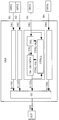
- optical amplifier splitter arrangement OAS will be explained by means of a functional description of the blocks shown in the figure. Based on this description, implementation of the functional blocks in the figure will be obvious to a person skilled in the art.
- the optical amplifier splitter arrangement OAS is used in a tree-like optical network consisting of the cascade connection of dedicated branches B1, B2, ..., Bi,...Bn and of the optical amplifier splitter arrangement OAS and of a common branch.
- the optical amplifier splitter arrangement OAS is coupled between a plurality of optical network users ONU1, ONU2, ..., ONUi, ..., ONUn and an optical line terminator OLT via the above mentioned dedicated branches and common branch respectively.
- the optical amplifier splitter arrangement OAS includes for each branch e.g. Bi, of the dedicated branches B1, B2,..., Bi, ..., Bn two basic parts :
- the optical splitter OS is coupled between all optical switches on/off SW ON/OFF1, SW ON/OFF2, ..., SW ON/OFFi, ..., SW ON/OFFn which are simular to the optical switch on/off SW ON/OFFi and the optical line terminator OLT.
- the optical amplifier splitter arrangement OAS enables upstream transmission in the optical network of information signals IN1, IN2, ..., INi, ... , INn from the optical network users ONU1, ONU2, ..., ONUi, ..., ONUn to the optical line terminator OLT.
- optical amplifier splitter OAS The principle working of the optical amplifier splitter OAS will be explained in the following paragraph with respect to a signal INi transmitted over a branch Bi, the working with respect to the other branches being identical.
- the optical amplifier OAi amplifies INi with a gain value Gi (not shown) and generates thereby an amplified information signal A-INi with a predetermined power level.
- the optical switch on/off SW ON/OFFi passes the amplified information signal A-INi when it is present, but interrupts the branch Bi when the amplified information signal A-INi is not present.
- the optical splitter OS combines all amplified information signals A-IN1, A-IN2, ..., A-INi, ..., A-INn simular to the amplified information signal A-INi according to a multiple access technique and generates thereby an outgoing optical signal OUT for application to the optical line terminator OLT.
- control means CTRLi is coupled to the OAi and the optical switch on/off SW ON/OFFi and controls :
- the gain setting data GSi, the gain tuning data GTi and the second electrical control signal CTRL-Bi can be determined in different ways. A few particular implementations to determine them are described in a functional way in the following paragraphs, but they are not shown in the figure to avoid overloading thereof.
- control means CTRLi further includes power detection means which via an optical tap draws off the information signal INi a small power part.
- the power detection means determines whether the information signal INi is present or is not present and determines the second electrical control signal CTRL-Bi as a result thereof.
- control means CTRLi further includes power measuring means.
- the same optical tap as above is used and the power measuring means measures the power of the information signal INi and determines the gain setting data GSi based thereon.
- an optical delay line (not shown) is coupled between the optical tap and the optical amplifier OAi.
- the optical delay line delays the information signal INi untill the optical amplifier OAi is adjusted.
- control means CTRLi further includes additional power measuring means. Via an additional optical tap, coupled between the optical switch on/off SW ON/OFFi and the optical splitter OS a small power part is drawn off the amplified information signal A-INi and the additional power measuring means measures the power of the amplified information signal A-INi and determines the gain tuning data GTi based thereon.
- optical amplifier OAi an erbium doped fibre amplifier
- semiconductor optical amplifiers are very good candidates to use in this implementation because of their low switch-on time. It is also remarked that these semiconductor optical amplifiers can be used to integrate the functions of the optical amplifier OAi and of the optical switch on/off SW ON/OFFi.
- the optical amplifier splitter arrangement OAS includes an optical network terminator NTOAM (not shown) for performing operation and maintenance functions.
- the NTOAM is coupled to the optical line terminator OLT, by means of also an additional optical tap, and to the control means CTRLi.
- the additional optical tap draws off the downstream signals which are sent from the optical line terminator OLT to the optical network terminators ONU1, ONU2, ..., ONUi, ..., ONUn a small powerpart and provides this power fraction to the optical network terminator NTOAM which captures special grant information out of these downstream signals.
- special grant information to realize time division multiple access is well known in the art.
- the optical network terminator NTOAM knows exactly when an information signal INi will be sent by an optical network user ONUi and when the information signal INi will be applied to the optical amplifier OAi.
- the special grant information is applied to the control means CTRLi which is now able to determine whether the information signal INi will be present or will not be present within a predetermined time interval and determines the second electrical control signal CTRL-Bi as a result thereof.
- Still another alternative implementation to determine the gain tuning data GTi, for each branch Bi is realised by including in the control means CTRLi, additional to measuring means to measure the power of an amplified information signal A-INi, also memory means to memorize the value of the measured power of the amplified signal. This value is used to determine the gain tuning data GTi for a following transmitted information signal INi.
- the power level unit included in the optical amplifier splitter arrangement OAS, is coupled between a control output of the optical splitter OS and the control means CTRLi associated with each branch Bi.
- the power level unit measures the power level of the outgoing optical signal OUT and provides the result thereof by means of electrical power level data to the control means CTRLi.
- the control means CTRLi is now able to determine the gain tuning data GTi if an information signal is present.
- optical splitter OS and all optical switches on/off SW ON/OFF1, SW ON/OFF2, ..., SW ON/OFFi, ..., SW ON/OFFn simular to the optical switch on/off SW ON/OFFi can be integrated in one optical switch.
- the outgoing optical signal OUT of the present optical amplifier splitter arrangement OAS has to be amplified in order to overcome a longe distance to the optical line terminator OLT.
- the outgoing optical signal OUT has no longer a bursty character like the information signals IN1, IN2, ..., INi, ..., INn have. In this way, a fast gain setting optical amplifier is no longer required for the amplification of the optical outgoing signal OUT and a standard optical amplifiers can be used.
Priority Applications (7)
| Application Number | Priority Date | Filing Date | Title |
|---|---|---|---|
| ES95202553T ES2167399T3 (es) | 1995-09-21 | 1995-09-21 | Disposicion para amplificar y combinar señales opticas y metodo para transmision corriente arriba realizada con ella. |
| DE69524751T DE69524751T2 (de) | 1995-09-21 | 1995-09-21 | Optische Verstärkungs-Kombinierungsanordnung und Verfahren zur Aufwärtsrichtungsübertragung unter Verwendung einer solchen Anordnung |
| EP95202553A EP0765045B1 (de) | 1995-09-21 | 1995-09-21 | Optische Verstärkungs-Kombinierungsanordnung und Verfahren zur Aufwärtsrichtungsübertragung unter Verwendung einer solchen Anordnung |
| AU65543/96A AU714781B2 (en) | 1995-09-21 | 1996-09-11 | Optical amplifier splitter |
| US08/714,342 US5754319A (en) | 1995-09-21 | 1996-09-16 | Optical amplifier combiner arrangement and method for upstream transmission realized thereby |
| CA002186149A CA2186149A1 (en) | 1995-09-21 | 1996-09-20 | Optical amplifier combiner arrangement and method for upstream transmission realised thereby |
| JP25167296A JP3842349B2 (ja) | 1995-09-21 | 1996-09-24 | 光増幅器結合器装置およびそれにより実現される上流伝送方法 |
Applications Claiming Priority (1)
| Application Number | Priority Date | Filing Date | Title |
|---|---|---|---|
| EP95202553A EP0765045B1 (de) | 1995-09-21 | 1995-09-21 | Optische Verstärkungs-Kombinierungsanordnung und Verfahren zur Aufwärtsrichtungsübertragung unter Verwendung einer solchen Anordnung |
Publications (2)
| Publication Number | Publication Date |
|---|---|
| EP0765045A1 true EP0765045A1 (de) | 1997-03-26 |
| EP0765045B1 EP0765045B1 (de) | 2001-12-19 |
Family
ID=8220648
Family Applications (1)
| Application Number | Title | Priority Date | Filing Date |
|---|---|---|---|
| EP95202553A Expired - Lifetime EP0765045B1 (de) | 1995-09-21 | 1995-09-21 | Optische Verstärkungs-Kombinierungsanordnung und Verfahren zur Aufwärtsrichtungsübertragung unter Verwendung einer solchen Anordnung |
Country Status (7)
| Country | Link |
|---|---|
| US (1) | US5754319A (de) |
| EP (1) | EP0765045B1 (de) |
| JP (1) | JP3842349B2 (de) |
| AU (1) | AU714781B2 (de) |
| CA (1) | CA2186149A1 (de) |
| DE (1) | DE69524751T2 (de) |
| ES (1) | ES2167399T3 (de) |
Cited By (6)
| Publication number | Priority date | Publication date | Assignee | Title |
|---|---|---|---|---|
| EP0989694A1 (de) * | 1998-09-23 | 2000-03-29 | Alcatel | Verfahren zur Ermittlung eines Schaltzeitpunktes |
| EP1037417A1 (de) * | 1999-03-17 | 2000-09-20 | Alcatel | Verfahren zur zentralen Steuerung eines Leitungsabschlusses in einem baumartigen Netz |
| EP1333612A2 (de) * | 2002-02-01 | 2003-08-06 | Samsung Electronics Co., Ltd. | Überwachungsschaltung des Lehrzeichens in einem passiven optischen Gigabit-Ethernet Netzwerk |
| WO2005029906A1 (en) * | 2003-09-15 | 2005-03-31 | Teknovus, Inc. | Method and apparatus for transmission control in an ethernet passive optical network |
| EP2288176A3 (de) * | 2000-05-30 | 2011-05-04 | Nortel Networks Limited | Mehrfachzugriffsystem für ein Kommunikationsnetzwerk |
| CN101459473B (zh) * | 2007-12-14 | 2012-01-25 | 华为技术有限公司 | 分光器、合光器和点到多点网络系统 |
Families Citing this family (23)
| Publication number | Priority date | Publication date | Assignee | Title |
|---|---|---|---|---|
| US6693033B2 (en) | 2000-02-10 | 2004-02-17 | Motorola, Inc. | Method of removing an amorphous oxide from a monocrystalline surface |
| AU2001264987A1 (en) * | 2000-06-30 | 2002-01-14 | Motorola, Inc., A Corporation Of The State Of Delware | Hybrid semiconductor structure and device |
| US6590236B1 (en) | 2000-07-24 | 2003-07-08 | Motorola, Inc. | Semiconductor structure for use with high-frequency signals |
| US6555946B1 (en) | 2000-07-24 | 2003-04-29 | Motorola, Inc. | Acoustic wave device and process for forming the same |
| US6493497B1 (en) | 2000-09-26 | 2002-12-10 | Motorola, Inc. | Electro-optic structure and process for fabricating same |
| US6638838B1 (en) | 2000-10-02 | 2003-10-28 | Motorola, Inc. | Semiconductor structure including a partially annealed layer and method of forming the same |
| US6501121B1 (en) | 2000-11-15 | 2002-12-31 | Motorola, Inc. | Semiconductor structure |
| US6559471B2 (en) | 2000-12-08 | 2003-05-06 | Motorola, Inc. | Quantum well infrared photodetector and method for fabricating same |
| US6673646B2 (en) | 2001-02-28 | 2004-01-06 | Motorola, Inc. | Growth of compound semiconductor structures on patterned oxide films and process for fabricating same |
| US6709989B2 (en) | 2001-06-21 | 2004-03-23 | Motorola, Inc. | Method for fabricating a semiconductor structure including a metal oxide interface with silicon |
| EP1271825A1 (de) * | 2001-06-25 | 2003-01-02 | Lucent Technologies Inc. | Verfahren und System zur Übertragung von multiplexierten optischen Nachrichten |
| US6531740B2 (en) | 2001-07-17 | 2003-03-11 | Motorola, Inc. | Integrated impedance matching and stability network |
| US6646293B2 (en) | 2001-07-18 | 2003-11-11 | Motorola, Inc. | Structure for fabricating high electron mobility transistors utilizing the formation of complaint substrates |
| US6693298B2 (en) | 2001-07-20 | 2004-02-17 | Motorola, Inc. | Structure and method for fabricating epitaxial semiconductor on insulator (SOI) structures and devices utilizing the formation of a compliant substrate for materials used to form same |
| US6498358B1 (en) * | 2001-07-20 | 2002-12-24 | Motorola, Inc. | Structure and method for fabricating an electro-optic system having an electrochromic diffraction grating |
| US6667196B2 (en) | 2001-07-25 | 2003-12-23 | Motorola, Inc. | Method for real-time monitoring and controlling perovskite oxide film growth and semiconductor structure formed using the method |
| US6589856B2 (en) | 2001-08-06 | 2003-07-08 | Motorola, Inc. | Method and apparatus for controlling anti-phase domains in semiconductor structures and devices |
| US6639249B2 (en) | 2001-08-06 | 2003-10-28 | Motorola, Inc. | Structure and method for fabrication for a solid-state lighting device |
| US6673667B2 (en) | 2001-08-15 | 2004-01-06 | Motorola, Inc. | Method for manufacturing a substantially integral monolithic apparatus including a plurality of semiconductor materials |
| JP4860137B2 (ja) * | 2004-11-12 | 2012-01-25 | 日本電気通信システム株式会社 | 光アクセスネットワーク方法及び光アクセスネットワーク並びに光アクセスネットワーク用光スイッチ |
| JP5301364B2 (ja) * | 2009-06-17 | 2013-09-25 | 日本電信電話株式会社 | 光アクセスシステムおよび光中継装置 |
| CN102577182B (zh) * | 2011-12-28 | 2014-11-05 | 华为技术有限公司 | 光线路终端及其处理放大自发辐射的方法 |
| JP2014096649A (ja) * | 2012-11-08 | 2014-05-22 | Toshiba Corp | ウイルス遮断システム |
Citations (4)
| Publication number | Priority date | Publication date | Assignee | Title |
|---|---|---|---|---|
| EP0425871A2 (de) * | 1989-10-30 | 1991-05-08 | Broadband Technologies, Inc. | Lichtwellenleiter-Übertragungssystem unter Anwendung von kontinuierlichem Abwärts- und Burstaufwärtsformat mit vorgegebenem Aufwärtsschutzband |
| EP0499065A2 (de) * | 1991-02-11 | 1992-08-19 | Alcatel SEL Aktiengesellschaft | Optisches Nachrichtenübertragungssystem für den Teilnehmeranschlussbereich mit optischen Verstärkern |
| EP0506163A1 (de) * | 1991-03-29 | 1992-09-30 | PIRELLI CAVI S.p.A. | Lichtwellenleiternachrichtenübertragungsleitung mit Schutzvorrichtung für optische Verstärker |
| EP0534433A2 (de) * | 1991-09-24 | 1993-03-31 | Nec Corporation | Optisches Regenerator-Relaissystem |
Family Cites Families (7)
| Publication number | Priority date | Publication date | Assignee | Title |
|---|---|---|---|---|
| DE3507064A1 (de) * | 1985-02-28 | 1986-08-28 | Standard Elektrik Lorenz Ag, 7000 Stuttgart | Optisches nachrichtenuebertragungssystem im teilnehmeranschlussbereich |
| US5153762A (en) * | 1990-03-19 | 1992-10-06 | General Instrument Corporation | Method and apparatus for recovering AM channell signals distributed on an optical fiber |
| EP0544975B1 (de) * | 1991-12-05 | 1997-10-22 | Alcatel | Verwaltungssystem von Zeitschlitzen |
| JP3320452B2 (ja) * | 1992-07-15 | 2002-09-03 | 沖電気工業株式会社 | 光中継器の監視制御方式 |
| US5241414A (en) * | 1992-08-21 | 1993-08-31 | At&T Bell Laboratories | Fault tolerant optical amplifier arrangement |
| US5392154A (en) * | 1994-03-30 | 1995-02-21 | Bell Communications Research, Inc. | Self-regulating multiwavelength optical amplifier module for scalable lightwave communications systems |
| US5610744A (en) * | 1995-02-16 | 1997-03-11 | Board Of Trustees Of The University Of Illinois | Optical communications and interconnection networks having opto-electronic switches and direct optical routers |
-
1995
- 1995-09-21 EP EP95202553A patent/EP0765045B1/de not_active Expired - Lifetime
- 1995-09-21 ES ES95202553T patent/ES2167399T3/es not_active Expired - Lifetime
- 1995-09-21 DE DE69524751T patent/DE69524751T2/de not_active Expired - Lifetime
-
1996
- 1996-09-11 AU AU65543/96A patent/AU714781B2/en not_active Ceased
- 1996-09-16 US US08/714,342 patent/US5754319A/en not_active Expired - Lifetime
- 1996-09-20 CA CA002186149A patent/CA2186149A1/en not_active Abandoned
- 1996-09-24 JP JP25167296A patent/JP3842349B2/ja not_active Expired - Fee Related
Patent Citations (4)
| Publication number | Priority date | Publication date | Assignee | Title |
|---|---|---|---|---|
| EP0425871A2 (de) * | 1989-10-30 | 1991-05-08 | Broadband Technologies, Inc. | Lichtwellenleiter-Übertragungssystem unter Anwendung von kontinuierlichem Abwärts- und Burstaufwärtsformat mit vorgegebenem Aufwärtsschutzband |
| EP0499065A2 (de) * | 1991-02-11 | 1992-08-19 | Alcatel SEL Aktiengesellschaft | Optisches Nachrichtenübertragungssystem für den Teilnehmeranschlussbereich mit optischen Verstärkern |
| EP0506163A1 (de) * | 1991-03-29 | 1992-09-30 | PIRELLI CAVI S.p.A. | Lichtwellenleiternachrichtenübertragungsleitung mit Schutzvorrichtung für optische Verstärker |
| EP0534433A2 (de) * | 1991-09-24 | 1993-03-31 | Nec Corporation | Optisches Regenerator-Relaissystem |
Cited By (13)
| Publication number | Priority date | Publication date | Assignee | Title |
|---|---|---|---|---|
| US6239887B1 (en) | 1998-09-23 | 2001-05-29 | Alcatel | Method to determine a switching moment and a line terminator, a control network unit and a network unit realizing such a method and a tree-like optical network including such a line terminator, such a control network unit or such a network unit |
| EP0989694A1 (de) * | 1998-09-23 | 2000-03-29 | Alcatel | Verfahren zur Ermittlung eines Schaltzeitpunktes |
| US7079536B1 (en) | 1999-03-17 | 2006-07-18 | Alcatel | Method to perform central control, a line terminator and an element controller realizing such a method and a tree-like network including such a line terminator and an element controller |
| EP1037417A1 (de) * | 1999-03-17 | 2000-09-20 | Alcatel | Verfahren zur zentralen Steuerung eines Leitungsabschlusses in einem baumartigen Netz |
| EP2288176A3 (de) * | 2000-05-30 | 2011-05-04 | Nortel Networks Limited | Mehrfachzugriffsystem für ein Kommunikationsnetzwerk |
| EP1333612A2 (de) * | 2002-02-01 | 2003-08-06 | Samsung Electronics Co., Ltd. | Überwachungsschaltung des Lehrzeichens in einem passiven optischen Gigabit-Ethernet Netzwerk |
| US7274874B2 (en) | 2002-02-01 | 2007-09-25 | Samsung Electronics Co., Ltd. | Idle-pattern output control circuit used in a Gigabit Ethernet-passive optical network |
| EP1333612A3 (de) * | 2002-02-01 | 2004-11-17 | Samsung Electronics Co., Ltd. | Überwachungsschaltung des Lehrzeichens in einem passiven optischen Gigabit-Ethernet Netzwerk |
| WO2005029906A1 (en) * | 2003-09-15 | 2005-03-31 | Teknovus, Inc. | Method and apparatus for transmission control in an ethernet passive optical network |
| US7630639B2 (en) | 2003-09-15 | 2009-12-08 | Teknovus, Inc. | Method and apparatus for transmission control in an ethernet passive optical network |
| CN1823547B (zh) * | 2003-09-15 | 2010-08-18 | 泰克诺沃斯公司 | 用于在以太无源光网络中进行传输控制的方法和装置 |
| KR101028057B1 (ko) * | 2003-09-15 | 2011-04-08 | 테크노버스, 인크. | 이더넷 패시브 광 네트워크 환경에서의 전송 제어를 위한방법과 장치 |
| CN101459473B (zh) * | 2007-12-14 | 2012-01-25 | 华为技术有限公司 | 分光器、合光器和点到多点网络系统 |
Also Published As
| Publication number | Publication date |
|---|---|
| EP0765045B1 (de) | 2001-12-19 |
| AU714781B2 (en) | 2000-01-13 |
| US5754319A (en) | 1998-05-19 |
| JPH09181686A (ja) | 1997-07-11 |
| CA2186149A1 (en) | 1997-03-22 |
| ES2167399T3 (es) | 2002-05-16 |
| DE69524751D1 (de) | 2002-01-31 |
| DE69524751T2 (de) | 2002-08-22 |
| AU6554396A (en) | 1997-03-27 |
| JP3842349B2 (ja) | 2006-11-08 |
Similar Documents
| Publication | Publication Date | Title |
|---|---|---|
| EP0765045B1 (de) | Optische Verstärkungs-Kombinierungsanordnung und Verfahren zur Aufwärtsrichtungsübertragung unter Verwendung einer solchen Anordnung | |
| US6201622B1 (en) | Optical network | |
| KR101391265B1 (ko) | 양방향 광학 증폭기 | |
| KR100724902B1 (ko) | 댁내 방송서비스 수용을 위한 수동형 광가입자망에프티티에이치 시스템 | |
| US7006282B2 (en) | Control system and method for an optical amplifier | |
| US8693889B2 (en) | Apparatus and methods for adaptively using signals to control a semiconductor optical amplifier (SOA) | |
| EP0859480A2 (de) | Breitbandiger optischer Verstärker mit gleichmässiger Verstärkung | |
| CN101572832A (zh) | 一种无源光网络拉远的方法及设备和系统 | |
| WO2020045185A1 (ja) | 光通信システム及び光通信方法 | |
| CN101350670B (zh) | 一种用于无源光网络中光信号的放大装置和方法以及光线路终端 | |
| US20230082934A1 (en) | Optical communication system and control method | |
| US6342958B1 (en) | Wavelength division multiplexed transmission system and transmitting method using the same | |
| JP2000151524A (ja) | 切替え時刻を決定する方法、そのような方法を実現する回線終端装置、制御ネットワ―クユニットおよびネットワ―クユニット、ならびにそのような回線終端装置、そのような制御ネットワ―クユニットまたはそのようなネットワ―クユニットを含むツリ―状光ネットワ―ク | |
| US8121476B2 (en) | All-optical CSMA/CD apparatus in base A ethernet and the method therefor | |
| US10299021B2 (en) | Optical signal amplification | |
| CN115664650A (zh) | 一种共纤量子密钥分配系统、方法及无源光网络 | |
| Slabbinck et al. | Evaluation of a superPON demonstrator | |
| CN117440267A (zh) | 一种pon olt模块、功率调整方法及存储介质 | |
| Rasztovits-Wiech et al. | Is a 10/2.5 Gbit/s extra-large PON far from reality | |
| JPH09205408A (ja) | 光バースト信号受信方式 | |
| KR20210031239A (ko) | 수동형 광 네트워크에서 미인증 회선의 차단을 위한 시스템 및 방법 | |
| JP2015100027A (ja) | 光増幅装置および光増幅装置のゲイン設定方法 | |
| JP2002064469A (ja) | 光ネットワーク | |
| van der Plaats et al. | Evolution-friendly upgrade of CATV networks towards a broadband full services access network | |
| MXPA97007189A (en) | Opt network |
Legal Events
| Date | Code | Title | Description |
|---|---|---|---|
| PUAI | Public reference made under article 153(3) epc to a published international application that has entered the european phase |
Free format text: ORIGINAL CODE: 0009012 |
|
| AK | Designated contracting states |
Kind code of ref document: A1 Designated state(s): BE DE ES FR GB IT NL SE |
|
| 17P | Request for examination filed |
Effective date: 19970926 |
|
| 17Q | First examination report despatched |
Effective date: 19991130 |
|
| GRAG | Despatch of communication of intention to grant |
Free format text: ORIGINAL CODE: EPIDOS AGRA |
|
| GRAG | Despatch of communication of intention to grant |
Free format text: ORIGINAL CODE: EPIDOS AGRA |
|
| GRAH | Despatch of communication of intention to grant a patent |
Free format text: ORIGINAL CODE: EPIDOS IGRA |
|
| RAP1 | Party data changed (applicant data changed or rights of an application transferred) |
Owner name: ALCATEL |
|
| GRAH | Despatch of communication of intention to grant a patent |
Free format text: ORIGINAL CODE: EPIDOS IGRA |
|
| GRAA | (expected) grant |
Free format text: ORIGINAL CODE: 0009210 |
|
| STAA | Information on the status of an ep patent application or granted ep patent |
Free format text: STATUS: THE PATENT HAS BEEN GRANTED |
|
| AK | Designated contracting states |
Kind code of ref document: B1 Designated state(s): BE DE ES FR GB IT NL SE |
|
| PG25 | Lapsed in a contracting state [announced via postgrant information from national office to epo] |
Ref country code: NL Free format text: LAPSE BECAUSE OF FAILURE TO SUBMIT A TRANSLATION OF THE DESCRIPTION OR TO PAY THE FEE WITHIN THE PRESCRIBED TIME-LIMIT Effective date: 20011219 Ref country code: BE Free format text: LAPSE BECAUSE OF FAILURE TO SUBMIT A TRANSLATION OF THE DESCRIPTION OR TO PAY THE FEE WITHIN THE PRESCRIBED TIME-LIMIT Effective date: 20011219 |
|
| REG | Reference to a national code |
Ref country code: GB Ref legal event code: IF02 |
|
| REF | Corresponds to: |
Ref document number: 69524751 Country of ref document: DE Date of ref document: 20020131 |
|
| PG25 | Lapsed in a contracting state [announced via postgrant information from national office to epo] |
Ref country code: SE Free format text: LAPSE BECAUSE OF FAILURE TO SUBMIT A TRANSLATION OF THE DESCRIPTION OR TO PAY THE FEE WITHIN THE PRESCRIBED TIME-LIMIT Effective date: 20020319 |
|
| REG | Reference to a national code |
Ref country code: ES Ref legal event code: FG2A Ref document number: 2167399 Country of ref document: ES Kind code of ref document: T3 |
|
| NLV1 | Nl: lapsed or annulled due to failure to fulfill the requirements of art. 29p and 29m of the patents act | ||
| PLBE | No opposition filed within time limit |
Free format text: ORIGINAL CODE: 0009261 |
|
| 26N | No opposition filed | ||
| NLV1 | Nl: lapsed or annulled due to failure to fulfill the requirements of art. 29p and 29m of the patents act | ||
| PGFP | Annual fee paid to national office [announced via postgrant information from national office to epo] |
Ref country code: ES Payment date: 20100924 Year of fee payment: 16 |
|
| PGFP | Annual fee paid to national office [announced via postgrant information from national office to epo] |
Ref country code: IT Payment date: 20100922 Year of fee payment: 16 |
|
| PG25 | Lapsed in a contracting state [announced via postgrant information from national office to epo] |
Ref country code: IT Free format text: LAPSE BECAUSE OF NON-PAYMENT OF DUE FEES Effective date: 20110921 |
|
| REG | Reference to a national code |
Ref country code: ES Ref legal event code: FD2A Effective date: 20130603 |
|
| PG25 | Lapsed in a contracting state [announced via postgrant information from national office to epo] |
Ref country code: ES Free format text: LAPSE BECAUSE OF NON-PAYMENT OF DUE FEES Effective date: 20110922 |
|
| REG | Reference to a national code |
Ref country code: FR Ref legal event code: GC Effective date: 20140717 |
|
| PGFP | Annual fee paid to national office [announced via postgrant information from national office to epo] |
Ref country code: DE Payment date: 20140922 Year of fee payment: 20 |
|
| PGFP | Annual fee paid to national office [announced via postgrant information from national office to epo] |
Ref country code: GB Payment date: 20140919 Year of fee payment: 20 Ref country code: FR Payment date: 20140919 Year of fee payment: 20 |
|
| REG | Reference to a national code |
Ref country code: DE Ref legal event code: R071 Ref document number: 69524751 Country of ref document: DE |
|
| REG | Reference to a national code |
Ref country code: GB Ref legal event code: PE20 Expiry date: 20150920 |
|
| PG25 | Lapsed in a contracting state [announced via postgrant information from national office to epo] |
Ref country code: GB Free format text: LAPSE BECAUSE OF EXPIRATION OF PROTECTION Effective date: 20150920 |