EP0763243B1 - Speichereinrichtung - Google Patents
Speichereinrichtung Download PDFInfo
- Publication number
- EP0763243B1 EP0763243B1 EP95920463A EP95920463A EP0763243B1 EP 0763243 B1 EP0763243 B1 EP 0763243B1 EP 95920463 A EP95920463 A EP 95920463A EP 95920463 A EP95920463 A EP 95920463A EP 0763243 B1 EP0763243 B1 EP 0763243B1
- Authority
- EP
- European Patent Office
- Prior art keywords
- data
- portals
- memory device
- portal
- memory
- Prior art date
- Legal status (The legal status is an assumption and is not a legal conclusion. Google has not performed a legal analysis and makes no representation as to the accuracy of the status listed.)
- Expired - Lifetime
Links
- 230000015654 memory Effects 0.000 claims description 70
- 238000000034 method Methods 0.000 claims description 45
- 230000033001 locomotion Effects 0.000 claims description 27
- 230000009897 systematic effect Effects 0.000 claims description 20
- 238000013500 data storage Methods 0.000 claims description 18
- 230000006870 function Effects 0.000 claims description 14
- 230000001902 propagating effect Effects 0.000 claims description 12
- 230000003068 static effect Effects 0.000 claims description 11
- 238000004364 calculation method Methods 0.000 claims description 7
- 230000005055 memory storage Effects 0.000 claims description 7
- 238000004891 communication Methods 0.000 claims description 3
- 229910052710 silicon Inorganic materials 0.000 claims description 2
- 238000005516 engineering process Methods 0.000 description 19
- 238000007906 compression Methods 0.000 description 7
- 230000006835 compression Effects 0.000 description 7
- 238000013461 design Methods 0.000 description 7
- 239000004065 semiconductor Substances 0.000 description 7
- 230000008901 benefit Effects 0.000 description 5
- 239000000758 substrate Substances 0.000 description 5
- 238000003491 array Methods 0.000 description 4
- 238000013144 data compression Methods 0.000 description 3
- 230000008569 process Effects 0.000 description 3
- 230000003134 recirculating effect Effects 0.000 description 3
- 238000012546 transfer Methods 0.000 description 3
- 230000005540 biological transmission Effects 0.000 description 2
- 238000010276 construction Methods 0.000 description 2
- 238000012937 correction Methods 0.000 description 2
- 230000003111 delayed effect Effects 0.000 description 2
- 238000010586 diagram Methods 0.000 description 2
- 230000007246 mechanism Effects 0.000 description 2
- 229910044991 metal oxide Inorganic materials 0.000 description 2
- 150000004706 metal oxides Chemical class 0.000 description 2
- 238000012986 modification Methods 0.000 description 2
- 230000004048 modification Effects 0.000 description 2
- 230000000737 periodic effect Effects 0.000 description 2
- 230000001172 regenerating effect Effects 0.000 description 2
- 230000003362 replicative effect Effects 0.000 description 2
- 238000011160 research Methods 0.000 description 2
- 230000004044 response Effects 0.000 description 2
- XUIMIQQOPSSXEZ-UHFFFAOYSA-N Silicon Chemical compound [Si] XUIMIQQOPSSXEZ-UHFFFAOYSA-N 0.000 description 1
- 230000003213 activating effect Effects 0.000 description 1
- 230000009118 appropriate response Effects 0.000 description 1
- 238000010367 cloning Methods 0.000 description 1
- 230000001934 delay Effects 0.000 description 1
- 230000005669 field effect Effects 0.000 description 1
- 230000002452 interceptive effect Effects 0.000 description 1
- 239000000463 material Substances 0.000 description 1
- 239000002184 metal Substances 0.000 description 1
- 239000000203 mixture Substances 0.000 description 1
- 238000012856 packing Methods 0.000 description 1
- 238000010422 painting Methods 0.000 description 1
- 230000009467 reduction Effects 0.000 description 1
- 230000008929 regeneration Effects 0.000 description 1
- 238000011069 regeneration method Methods 0.000 description 1
- 230000008439 repair process Effects 0.000 description 1
- 230000003252 repetitive effect Effects 0.000 description 1
- 239000010703 silicon Substances 0.000 description 1
- 230000001960 triggered effect Effects 0.000 description 1
- 230000000007 visual effect Effects 0.000 description 1
Images


Classifications
-
- H—ELECTRICITY
- H04—ELECTRIC COMMUNICATION TECHNIQUE
- H04N—PICTORIAL COMMUNICATION, e.g. TELEVISION
- H04N7/00—Television systems
- H04N7/08—Systems for the simultaneous or sequential transmission of more than one television signal, e.g. additional information signals, the signals occupying wholly or partially the same frequency band, e.g. by time division
-
- G—PHYSICS
- G11—INFORMATION STORAGE
- G11C—STATIC STORES
- G11C19/00—Digital stores in which the information is moved stepwise, e.g. shift registers
-
- G—PHYSICS
- G11—INFORMATION STORAGE
- G11C—STATIC STORES
- G11C19/00—Digital stores in which the information is moved stepwise, e.g. shift registers
- G11C19/18—Digital stores in which the information is moved stepwise, e.g. shift registers using capacitors as main elements of the stages
- G11C19/182—Digital stores in which the information is moved stepwise, e.g. shift registers using capacitors as main elements of the stages in combination with semiconductor elements, e.g. bipolar transistors, diodes
- G11C19/188—Organisation of a multiplicity of shift registers, e.g. regeneration, timing or input-output circuits
-
- H—ELECTRICITY
- H04—ELECTRIC COMMUNICATION TECHNIQUE
- H04N—PICTORIAL COMMUNICATION, e.g. TELEVISION
- H04N21/00—Selective content distribution, e.g. interactive television or video on demand [VOD]
- H04N21/20—Servers specifically adapted for the distribution of content, e.g. VOD servers; Operations thereof
- H04N21/23—Processing of content or additional data; Elementary server operations; Server middleware
- H04N21/231—Content storage operation, e.g. caching movies for short term storage, replicating data over plural servers, prioritizing data for deletion
-
- H—ELECTRICITY
- H04—ELECTRIC COMMUNICATION TECHNIQUE
- H04N—PICTORIAL COMMUNICATION, e.g. TELEVISION
- H04N7/00—Television systems
- H04N7/10—Adaptations for transmission by electrical cable
-
- H—ELECTRICITY
- H04—ELECTRIC COMMUNICATION TECHNIQUE
- H04N—PICTORIAL COMMUNICATION, e.g. TELEVISION
- H04N7/00—Television systems
- H04N7/16—Analogue secrecy systems; Analogue subscription systems
- H04N7/173—Analogue secrecy systems; Analogue subscription systems with two-way working, e.g. subscriber sending a programme selection signal
- H04N7/17309—Transmission or handling of upstream communications
- H04N7/17336—Handling of requests in head-ends
Definitions
- the present invention relates generally to memory devices and methods of storing and accessing data. More particularly, the invention concerns storage of data streams in a manner that establishes a systematic relationship between the data itself and points used for accessing the data, to provide independent and extremely efficient access to, and dissemination of, the stored data streams.
- a system offering the wide range of information-related services just described should preferably be able to (i) store very large quantities of data at an affordable cost per bit; and (ii) provide for efficient retrieval of the data with a minimal contention between users for any portion of the data.
- Memory devices are advantageously utilized for storing information (e.g., information in digital or analog form).
- information e.g., information in digital or analog form.
- the types of information capable of being stored can include video and audio information (e.g., movies, video games, television and other entertainment programs), educational information and programs, scientific and other research-related database information, consumer catalog and home-shopping information, and the like, and are hereinafter referenced generically as "information" or "titles”.
- audio information such as speech or musical compositions
- visual information such as paintings and photographs
- audiovisual information such as movies, television shows and video games.
- a sequential group of still pictures is connected together on a long strip of photographic film.
- the still pictures are moved past a light source in sequence and at a certain speed, and the resulting images are focused onto a screen while the audio portion of the movie is output over speakers. These resulting images will appear to the viewer to be moving.
- music stored on magnetic tape can be "played back” by moving the magnetic tape serially past a playback head of a tape player.
- digitally stored data may be stored in a memory and accessed in serial fashion to obtain the same result achieved by the more traditional storage formats mentioned above.
- an assemblage of stored digital data if "played back" in serial fashion, can reproduce any of the above types of information.
- a few of the many types of mechanisms used to store digital data are introduced here just by way of example. They include shift registers, charge coupled devices (CCDs), delay lines, read-only memory (ROM) and random-access memory (RAM).
- Fig. 1A shows a typical shift register arrangement.
- the shift register 10 is composed of a series of D-flip-flops 11.
- the number of flip-flops provided is variable and depends upon the number of bits N to be stored.
- clock pulses input at clock input 12 cause the data at the inputs D to transfer to the outputs Q.
- This clocking causes data supplied bit by bit at the data input 13 to shift right by one flip-flop.
- the data is output bit by bit at the data output 14.
- the shift register illustrated in Fig. 1B is another example of a register, namely a recirculating shift register manufactured by Signetics in 1972.
- the shift register comprises an input 20 for data, an input selector 21, a data storage selector 22 composed of logic gates, a shift register 23, a device selector 24, an output selector 25, clock inputs 26, 27, a write control 28, a read control 29, and a data output 30.
- the shift register is activated by inputting high signals at the device selector 24.
- a write enable signal is input to the write control 28, while clock input 26 receives clock pulses.
- the data to be stored is fed to the input 20, thereby inputting the data to be stored.
- the data storage selector 22 recirculates the stored data through the shift register 23, thereby storing the data.
- a read signal to the read control 29 and clock pulses to the clock input 27 trigger the output selector 25 to output the data stored in the shift register at output 30. Since the output operation does not damage the recirculating data, the output operation can be performed repeatedly for the same stored data. To alter the data stored in the register, it must be over-written with new data by a write operation, as described above.
- the storage capacity for this type of shift register is 512 or 1024 binary digits (bits).
- Prior art delay lines such as the one shown in Fig. 1C, are composed of a silicon substrate 31, a signal input 32, several signal taps 33 spaced equally along the substrate 31, and a signal output 34.
- An electrical signal entering the delay line at the input 32 propagates through the substrate 31 at a fixed, predetermined velocity. While propagating, the signal passes by each of the several taps 33, which can be used to access the data. Thus, it becomes possible to delay the propagating signal a predetermined amount of time by passing it through the delay line and then selecting an appropriate tap that corresponds to the amount of desired delay. Once the propagating signal reaches the end of the substrate, it is output from the delay line at 34.
- Figs. 1D and 1E show a CCD, where Fig. 1D is a schematic circuit diagram and Fig. 1E is a structural diagram.
- the CCD is composed of metal oxide semiconductor field effect transistors (MOSFETs) 40 connected in series.
- Amplifiers 41, 42 also composed of MOSFETs, are provided on the CCD input and the CCD output, respectively.
- the CCD operates similarly to the shift register (see Fig. 1A) in that a signal enters the CCD at the input 41 and progresses through the CCD from MOSFET to MOSFET in accordance with clock pulses supplied at clock inputs 43 and 44. After proceeding through the series of MOSFETs 40, the signal exits the CCD at output 42.
- the individual MOSFETs are formed by placing metal contact layers 45 at appropriate locations on a semiconductor substrate 46.
- FIG. 1F A typical RAM is illustrated in Fig. 1F.
- an array of memory cells 50 is connected to respective series of row selectors 51, column selectors 52, write amplifiers 53, and sense amplifiers 54.
- a data load operation a particular cell to be written to is selected by providing the cell's appropriate column and row address, using the selectors 51 and 52.
- the data to be written to that cell is then input to the array 50 via the write amplifiers 53. Given the prior selection operation, however, the data is stored only in the selected cell.
- a particular cell to be read is again selected by providing appropriate column and row addresses via the selectors 51 and 52. The data is then copied out from the array 50 via the sense amplifiers 54.
- Fig. 1G illustrates a typical ROM.
- the structure is very similar to that of the RAM just described.
- An array of pre-set memory cells 60 is connected to respective series of row selectors 61, column selectors 62 and sense amplifiers 63. Operation of the ROM proceeds as described with respect to the data read operation of the RAM illustrated in Fig. 1F.
- data stored digitally in a computer memory also suffers from limitations on access and dissemination. For instance, in an Input/Output operation performed by a computer, the computer must repeatedly perform complex, multi-step operations to access, move and output the desired data in small increments. Also, output using known addressing techniques is a dedicated operation, in that it is limited to one single destination at any given time. As a result, only one end user at a time has access to the output data. Additionally, digital storage of audio-visual information has not been widely practiced, at least in part because the above limitations render it economically unfeasible.
- EP-A-0 596 656 discloses a programmable clock skew adjustment circuit in which the output of each stage of a ring shift register is a phase of a desired clock signal and is an input to a multiplexer that can selectively provide one of the desired clock phases.
- COMPUTER NETWORKS AND ISDN SYSTEMS 22 (1991), 1991, North Holland, SINCOSKIE: "System architecture for a large scale video on demand service” describes a disk assembly in which the relative positions of the disk heads are fixed. The motion of the arm holding the disk heads is a slow spiral from the outside toward the center of the disk. When a head reaches the center of the disk, the arm moves rapidly to the outside of the disk and repeats.
- the memory devices according to the present invention borrow from the above philosophy of outputting data in a serial and sequential manner to convey useful information, e.g., a motion picture.
- the data output from such a memory device can be used to produce a moving picture or the like from, essentially, sequential frames or their equivalent.
- the data is stored in a cyclical, systematic arrangement. In other words, once the data is input into the memory device, the data and some appropriate point of data access will repeatedly coincide.
- the location of the data can be computed, e.g., by knowing the present or past location of at least some part of the data.
- access to the data is not limited to a single scheduled output. Rather, according to the invention, there can be many output ports associated with one and the same set of stored data. These plural output ports permit independent, simultaneous access to the stored data. Also, these plural output ports can be configured to allow data cloning. Thus, the present invention provides for extremely efficient and powerful methods of data access and dissemination.
- the memory devices of the present invention can be designed in several different ways, as long as linkage between data and portals is assured. But it is not material how such linkage is achieved. For instance, according to one design, the memory device circulates data either through or past fixed portals. According to another, the data is stored in fixed address locations and the portals are moved from address to address. These and other alternative designs will be discussed in greater detail below in the Detailed Description.
- Preferred embodiments of the invention utilize semiconductor memory technology in order to implement the memory devices.
- semiconductor solutions are described below in the section entitled "Specific Embodiments of the Invention”.
- Another set of embodiments, also described below, utilizes memory storage media capable of confining propagating waves in order to implement the memory devices.
- Fig. 2 shows a memory device that is capable of storing data information, i.e., titles of various sorts.
- the device is constructed of a plurality of data storage devices 2, together forming a storage unit 1, and a plurality of portals 3.
- the portals 3 are dispersed around the storage unit 1 in a manner that can be described by means of modular arithmetic.
- the memory device is configured to establish relative movement between data stored in the storage unit and the portals 3.
- the storage devices 2 are arranged in the storage unit 1 in series fashion to form a circulating structure.
- This structure can take the form of an endless loop or ring, as shown in Fig. 2.
- the specific form chosen, however, is not particularly important, as long as the structure is systematic and provides a predictable arrangement of storage devices 2.
- the arrangement of storage devices 2 is defined in accordance with modular arithmetic. Modular arithmetic will be explained below, in conjunction with the detailed discussion of the portals 3.
- Fig. 2 shows six storage devices 2 connected into the ring structure. (As will become more apparent below, the number of storage devices 2 in an actual, commercial embodiment would be far greater than this. Only six are shown in order to render description of the invention simpler and clearer.) As will be discussed in descriptions of various implementations, below; the storage devices 2 can be selected from a wide variety of existing technologies. Currently, the most preferable hardware options are various types of semiconductor memory, e.g., shift registers, delay lines, CCDs, RAMs, ROMs and non-volatile memories of various types. Advances in technology will surely expand the list of available options.
- semiconductor memory e.g., shift registers, delay lines, CCDs, RAMs, ROMs and non-volatile memories of various types. Advances in technology will surely expand the list of available options.
- the portals 3 are connected to the storage unit 1 at various locations. In Fig. 2, the portals 3 are connected into the ring and alternate with storage devices 2. However, as with the storage devices, the particular form of connection is not important to the invention. Rather, it is important that the portals 3 are arranged in a systematic and predictable manner, and that they are configured to allow data to enter or exit (or both enter and exit) the storage unit.
- the arrangement of portals 3 is defined by modular arithmetic.
- Modular arithmetic as defined by Merriam-Webster Inc., is the "arithmetic that deals with whole numbers where the numbers are replaced by their remainders after division by a fixed number.”
- the arrangement of portals 3 is defined as follows: P i ⁇ P i+M , where
- Arranging the portals according to modular arithmetic renders access to data stored in the memory device calculable and reproducible.
- the benefits of the systematic nature of the arrangement will become apparent below.
- the portals 3 shown in Fig. 2 are each constructed as data replicators, such that, if selected, each portal performs both a replicating and an outputting function. This is indicated by the arrows shown on each of the signal paths 4 and 5 emanating from each portal 3.
- the arrows on signal paths 4 indicate data that continues circulating in the ring.
- the arrows on output signal paths 5 indicate data which is output from the ring. This is the preferable arrangement.
- the memory device can be constructed with non-replicating portals 3 and separate data replicators (not shown), which merely replicate the data stored in the device 1 but do not output it from the ring. Examples of hardware that can be used as portals 3 include latches, logic gates, regenerators and amplifiers.
- the memory device includes a means which forces portals 3 and data stored in the storage unit 1 to move relative to one another.
- the arrangement shown in Fig. 2 is one in which the data move and the portals 3 are fixed.
- clocking mechanism In digital arrangements, the means which establish the relative movement would be embodied by some form of clocking mechanism.
- Types of clocks easily adapted to a memory device according to the present invention include n-phase clocks, timing generators, address generators, data multiplexers, and microprocessors.
- Fig. 2 shows a controller 6 connected to the storage unit 1.
- the controller 6 is connected via signal control lines to respective portals 3.
- the controller 6 is configured to control data traffic at the portals 3, e.g., by selecting among data portals 3 in accordance with an externally supplied control signal 8.
- Data traffic includes either the input of data into the storage unit 1 via the portals, or the output of data from the storage unit 1 via the portals.
- the controller 6 establishes and regulates connections between the data portals 3 and signal lines 7.
- the signal lines 7 in Fig. 2 are indicated by the arrows as being output lines that transport replicated data out from the unit 1. However, the signal lines 7 can also be used for inputting data into the unit 1.
- the memory device is utilized for inputting data, for storing data and for outputting data.
- data to be stored is presented to some portal 3 in the ring, e.g. portal number 1.
- portal number 1 Once the portal number 1 is activated, the data is fed into the storage unit via the portal number 1 preferably as a sequential data stream. Any data previously existing in the ring is thereby over-written.
- the input operation is completed when all of the data desired to be stored has entered the storage unit 1 via the portal.
- the data is input in serial fashion, starting with the beginning of the movie and ending with the data corresponding to the closing credits.
- the data may be input in a time-division multiplexed or space-division multiplexed manner. This can be achieved, for example, by selecting more than one portal, e.g., the portals numbered 1 and 4, at predetermined relative times, for example, simultaneously.
- the controller 6 can, but need not, be used during the input operation. If the controller 6 is used, the controller 6 selects one of the signal lines 7 and one of the portals 3, and controls the input of data from the selected line 7 to the storage unit 1 via the selected portal 3. If the controller 6 is not used, an input line is simply connected directly to one or more portals 3 during the input operation.
- a cyclical arrangement is one in which, even though, en route, the data may be processed (e.g., error-corrected, error-proofed, modulated, encoded, decoded, encrypted, decrypted, etc.), branched, diverted, or otherwise acted upon, eventually, the data (or an appropriate facsimile or correlate thereof) and an appropriate point (such as a portal) in the memory structure will again coincide.
- the point in the memory structure may be stationary, while the data is kept in motion.
- the data can be held fixed while the point in the memory structure is moved.
- both the data and the points can be moved, relative to some third position of reference. Embodiments employing each of the above variations will be described in greater detail later in the specification.
- Fig. 2 shows a cyclical arrangement of stored data in which the data moves relative to fixed portals 3. More specifically, the data circulates in a ring structure, passing from one storage device 2 to the next, and so forth. If the portals 3 are connected into the ring, as shown in Fig. 2, they pass the data from one storage device 2 to the next during storage but otherwise remain passive. Alternatively, the portals 3, equally well, can be appended onto the ring, such that, during storage, the data stream passes directly from one storage device 2 to the next without passing through the portals 3.
- the fidelity of the stored data is maintained while the data circulates in the ring. As such, the data circulates in the same order in which it was input into the ring. Thus, if the ring has been loaded with data corresponding to a movie title, the movie title data circulates continuously through the ring, head following tail. As viewed from a specific point on the ring (e.g., some given portal 3), the data repeatedly passes by in the fashion in which it was loaded.
- the rate of circulation is determined by the frequency of the clock used by the memory device, as described above.
- the clock can also be used to alter the rate of circulation, if desired. For instance, it may be desirable to provide an arrangement wherein the relative movement between the stored data and the data portals is intermittent rather than continual. Applications conducive to intermittent data progression include video games and electronic catalogs. Movies, television programs, music and the like are preferably stored using continual (i.e., uninterrupted) data movement.
- one of the portals 3 is selected by the controller 6 as commanded by the control signal 8.
- one of the signal lines 7 is selected as an output line.
- the output operation then preferably proceeds by reproducing the stored data at the selected portal and delivering the reproduced data to the selected output line 7, so that the data may be routed to an appropriate destination. No further control is needed; once the appropriate portal is selected and the output operation commences, the stored data stream simply "flows out", i.e., is reproduced and delivered as it passes the selected portal.
- the output rate simply matches the rate of circulation of the data within the ring (assuming the portals operate at real time).
- the controller 6 may sever the connection between the selected portal 3 and the selected output line 7.
- non-selected portals simply pass the data within the ring, without reproducing it, on to the next storage device 2, as described above.
- the decision of which portal to select is governed by the momentary, current location of the stored data stream relative to the portals 3. For instance, if the stored data represents a movie title or television program, and it is desired to output it from its beginning, a portal is selected which lies an appropriate distance downstream of the current location of the beginning of the title/program.
- the momentary, current location can be calculated, given the predictable arrangement of the portals around the ring and the known rate of circulation of the data (or comparable parameters).
- the ability to compute a desired portal relative to data is a feature of the invention which is not characteristic of outputs of standard electronic devices (e.g., prior art shift registers, delay lines, CCDs, and so forth).
- the calculated portal number assumes a quality more commonly associated with an Input/Output operation performed by a computer.
- a single computation provides access to an entire stream of stored data, not just one data unit.
- the provision of plural data portals permits overlapping output sequences not achievable by standard I/O operations.
- this feature also distinguishes the present invention over known information distribution systems, such as local area networks (LANs, e.g., Token Ring, Ethernet), wide area networks (WANs), metropolitan area networks (MANs), and cable television systems.
- LANs local area networks
- WANs wide area networks
- MANs metropolitan area networks
- cable television systems In these systems, calculation of a portal has no relationship with input/output operations. Rather, these systems require cumbersome scheduling, addressing and routing schemes, to permit users to find and
- a first data portal 3 (e.g., data portal number 6) is selected for outputting the data at a first moment in time.
- the controller 6 controls the output such that the data is replicated and routed out from the storage unit 1, via a first selected output line 7, to a desired first end-user destination.
- the selected output line 7 thus carries the data, e.g., movie title, television program, etc., out in its sequential order as a first data stream.
- the controller 6 again calculates which portal should be selected for outputting the data at the second moment in time.
- the controller 6 then replicates and routes the data as a second data stream from the second selected data portal (e.g., portal number 2), via a second output line 7, to the second end-user destination.
- the calculation would provide for selecting the next available portal, here portal number 1.
- portal number 1 the next available portal
- the end user would not perceive the resulting delay.
- the time delay defining intervals between consecutive portals might be chosen to be, e.g., anywhere between 5 minutes, the best estimate of current human patience, and 1/30th of a second, the current refresh rate between television frames.
- the intervals between portals would be determined primarily by balancing grade of service with cost of the service.
- the stored data is replicated at each selected portal, and the portals operate independently, there is no requirement that output of the second data stream be delayed until the first data stream has been completely output.
- the data streams being output may be staggered, i.e., partially overlap.
- the title could be output to six different end-user destinations at once if the portals were each activated one after another.
- the signal lines 7 may be controlled in such a way that one given data stream branches to multiple end users. As such, the number of staggered "playbacks" of the stored title is further increased by providing simultaneous playback to different end-user destinations of any or all of the staggered "playbacks".
- the present invention provides an extremely powerful method of accessing data. Further, since the data streams (accessed as described and further cloned if desired) can be routed to a practically unlimited number of customers, the present invention provides an extremely efficient method of data dissemination.
- the design of the memory device described above implies that digital information will be circulating in a loop and that portal locations are fixed at given locations on the loop. According to the invention, however, it does not matter whether the data moves and the portal location is static, or the portal location moves and the data is static (or whether both move relative to a third chosen location). All these alternative designs perform the required functionality of a memory device.
- Figures 3 and 4A-4D inclusive illustrate the moving output ports (address) design.
- Figures 2 and 5A-5D illustrate the moving data alternative.
- Figures 6 and 7A-7D inclusive illustrate movement of both the ports and the data.
- Fig. 3 shows an alternative where the data forming a title 100 is held fixed in time in a data memory. As shown, the title 100 is subdivided into numerous individual blocks 1 to n and stored. Each block is a sequential segment of data. Preferably, each block of data is associated with one portal 101. Fig. 3 also shows a control device 102, which is used to select data blocks by activating appropriate portals 101.
- the control device 102 activates the portal 101 associated with data block 1.
- the data in block 1 travels via signal line 103 to the control device 102, which transfers data block 1 to an output line 104.
- the control device 102 will cause the next portal 101 in the sequence to be read. In this case, it is the portal associated with block 2.
- the control device will activate one portal after another, such that the output portal being activated changes with time.
- the data stored in the data memory is held fixed, while the portals used for accessing the title data move.
- FIGs. 4A-4D show an implementation of the fixed data, moving portals alternative.
- Figure 4A depicts a group of "N" memories 110. Each memory has a capacity of eight cells (a cell being any arbitrary amount of data).
- the configuration of data relative to output port 1 (see reference number 111), shown in figure 4A, corresponds to a reading operation of the data D1 held in the first cell of the first memory 1.
- Figure 4B shows the results as the second piece of data D2 held in the second cell of memory 1 is being read. This process continues until the data D8 in the eighth cell of memory 1 is read, as shown in Fig. 4C. Before the next piece of data is read, the "pointer" in the column of cells is then reset to the position associated with the first cell.
- the output port 1 is moved to the "next" memory 2. This is shown in Fig. 4D. This process continues until the full data stream has been accessed and output. Once the "last" piece of data is output, the output port 1 is again free to be reset to the initial memory cell location and to commence reading the data stream D1-DN from the beginning. If the memory structure is fully utilized, the "last" piece of data DN should be stored in cell number 8 of memory N. However, the "last" piece of data may be held in some previous location in memory, for instance, cell 3 of memory N-1.
- the control device operates according to a programmed sequence defining the sequence in which the portals 101 are accessed.
- This programmed sequence can be determined by an external control signal 105 or can be stored internally in the control device itself. If stored internally, the external control signal 105 may still be used, e.g., for selecting between several different stored sequence programs.
- the data memory used in this alternative can be any of a number of memory storage devices including dynamic RAM, static RAM, and pseudo static RAM. Further, there is no limit on the size of a data block. For example, one data block, as shown in the figure, can represent a complete RAM, a sector in RAM or even just a bit.
- the portals 101 can be constructed from logic gates, gate arrays, programmable logic arrays, etc.
- the control device 102 can be made from a number of devices including logic gates, gate arrays, microprocessors, and sequencers.
- FIG. 2 showed one memory arrangement in which moving data is accessed by fixed portals.
- FIGs. 5A-5D show one possible implementation of the moving data, fixed portals alternative.
- Figure 5A shows the configuration of title data 115 relative to output port 1 (see reference numeral 116) when the data D1 held in the first cell of the first memory 1 is being output. After the first piece of data D1 is read, the data D1-DN are transferred, as shown in figure 5B, such that the next piece of data D2 can be read.
- Figure 5C shows the data position once eight read operations have occurred.
- Figure 5D shows the relative position of the data to the output port 1 while DN, the final piece of data in the data stream, is being read.
- Fig. 6 shows an alternative where the data forming titles 120 and 130 are moving in time in respective data memories.
- the title 120 subdivided into blocks 1 to n, moves in time much in the same manner as described with respect to Fig. 2.
- the title 130 also subdivided into blocks 1 to n, moves in time within individual storage sub-units.
- Such an arrangement would exist, for example, if each storage sub-unit were constructed of a recirculating shift register, as described with respect to Fig. 1B.
- the arrangement of Fig. 6 is shown with one portal 121 or 131 associated with each block of data stored in the respective data memories.
- the control device 122 activates the portal 121 associated with data block 1 of that title.
- the data in block 1 travels via signal line 123 to the control device 122, which transfers data block 1 to an output line 124.
- the control device 122 will cause the next portal 121 in the programmed output sequence to be read. In this manner, the control device will activate one portal after another, such that the output portal being activated changes with time. Since the data blocks forming title 120 are also moving, the location of the data blocks also changes with time.
- FIGs. 7A-7D show one possible implementation of the moving data, moving portals alternative.
- output port 1 (see reference numeral 141) is always associated with memory 1.
- Figure 7A shows the configuration of title data 140 relative to output port 1 when the data D1 held in the first cell of the first memory 1 is being output. After the first piece of data D1 is read, the data D1, D9, D17...DN are transferred as shown in Figure 7B. The "pointer” is moved to the next memory cell in the same memory 1, to read data block D2.
- Figure 7C shows the data position after eight read operations, corresponding to D1-D8, have occurred, and the "pointer" has moved completely up the column of cells of memory 1.
- Figure 7D shows the device during the next subsequent read operation.
- the "pointer” is reset to the bottom of the column of data cells of memory 1. Also, by this time, the data forming title 120 has been completely shifted over by one memory. Thus, e.g., the data formerly held in memory 2 is shifted into memory 1, and the data formerly held in memory 1 is shifted into memory N. The "pointer” now begins reading up the column of memory 1 once again, but now reads the next set of data D9-D16. This process continues until the data D1 finally returns to memory 1.
- the data memory in this third alternative can be constructed, e.g., of circulating shift registers, charge coupled devices, or RAM controlled by data sequencers and the like.
- the control device can be implemented through microprocessors, data sequencers, logic gates, gate arrays, etc.
- the hardware design options for storing and accessing data according to the present invention can be chosen from a variety of existing technologies.
- the most preferable memory device hardware options are various types of semiconductor memory. Advances in technology will surely expand the list of available options.
- Fig. 8A shows a long series of clocked shift registers 151 connected to form a ring 150.
- the ring 150 is constructed such that an entire title is capable of being stored on the ring. Typically, to store a two-hour movie, using MPEG2 as a data compression method, the ring should be able to store approximately 180Gbits.
- the ring 150 is clocked by a clock source 152 which governs the rate of circulation of the data around the ring.
- the ring 150 is preferably clocked at such a rate to deliver (i.e., output) the title at a rate required by the receiver.
- Fig. 8B illustrates one possible such embodiment in which two parallel rings are constructed, each comprising clocked shift registers 151 connected in series.
- Fig. 8C illustrates an embodiment in which shift registers 151 are interconnected in series and in parallel to form the ring 150.
- the rate required is determined largely by the requirements imposed by the service provider.
- the data forming the title passes through the shift registers 151 serially as a sequential bit stream.
- the data is passed from one register 151 to the next in a manner explained in greater detail below.
- the access to the title stored in the ring 150 is obtained via the data ports 153.
- the ports 153 are preferably composed of logic circuitry 160-162.
- each port 153 has an input for receiving a bit stream input 154. Data for a new title is inserted into the ring 150 via inputs 154.
- each port 153 also has an output 155 for copying the bit stream circulating in the ring 150.
- the number (spacing) of ports 153 included in the ring 150 is based on an efficiency determination, balancing overall cost against access time.
- the spacing of the ports 153 defines the time intervals between permissible data access, and thus determines, in part, the waiting time between a subscriber request and fulfillment. If the title is accessible in sufficiently small increments, the delay time is imperceptible by humans.
- regenerators 156 can be inserted periodically in the ring 150 such that the data stream stored in the ring is regenerated as it passes through the regenerator.
- Fig. 8E shows in greater detail an embodiment in which the regenerator 156 is formed as a data checker 156' inserted between the registers 151.
- Each data checker 156' preferably contains logic circuitry 163-165 as well as a decoder 166 and an encoder 167. These are preferably a Reed-Solomon decoder and a Reed-Solomon encoder, respectively.
- the decoder 166 receives the data stream at an input, outputs any errors detected via an output 168, and outputs the decoded data to the logic circuitry 163-165.
- the output 168 leads to operational surveillance units.
- the data stream is input into the encoder 167 and is output as an encoded data stream to the next following shift register 151. Regeneration occurs as the bit stream passes through the Reed-Solomon decoders/encoders. Thus, errors can be corrected and/or brought to the attention of surveillance equipment.
- stored data can be processed in other useful ways known to those skilled in the art.
- data can be encoded or encrypted.
- Data would be encoded to provide means to ensure its reliability and to facilitate access to it.
- Data would be encrypted to prevent unauthorized access to and use of the data.
- data may be compressed.
- compression schemes include MPEG, fractal and variable data rate coding.
- MPEG currently the most common scheme used in the telecommunications industry, uses a discrete cosine transform and is a lossy compression scheme.
- MPEG provides a compression ratio of approximately 38:1.
- Fractal compression techniques which have only recently become viable, typically provide compression ratios of approximately 1500:1. References describing image compression techniques include W.B Pennebaker et al., JPEG (Reinhold, New York, NY, 1993); M.F. Barnsley et al., Fractal Image Compression (A.K.
- each ring is structured to allow data to be placed into the ring and copied from the ring. Further, each ring is able to detect and repair errors automatically. If excessive errors arise, this fact is signalled to the surveillance equipment, such that the ring can be taken temporarily out of service and repaired.
- the details of construction of the circuitry of the ring 150 are not particularly important in the present invention.
- the shift registers 151 can be constructed simply of standard logic circuits.
- the logic family for consideration of shift registers includes Emitter Coupled Logic (ECL), Transistor Transistor Logic (TTL), and Metal Oxide Semiconductor (MOS).
- ECL Emitter Coupled Logic
- TTL Transistor Transistor Logic
- MOS Metal Oxide Semiconductor
- a memory device may be implemented through the utilization of off-the-shelf shift registers.
- the MOS-type shift register is preferred, due to its larger memory size.
- the above embodiment is an example of a memory device in which the data portals are fixed and the stored data stream is moved through the shift registers 151 and through the data portals 153.
- a further, preferred alternative for embodying the memory device is to employ CCDs 171 (Charge-Coupled Devices) as the registers 151, as shown in Fig. 9, to form a ring memory device 170. If the ring 170 is constructed using CCDs 171, then each CCD 171 must be pumped by a clock source 172. Further, some form of regenerating means 176 must be coupled between each CCD 171. Possibilities for the regenerating means 176 include logic gates, as above. The individual CCDs simply function as registers in this embodiment, and the ring memory device 170, overall, functions similarly to the ring memory device 150 described with reference to Fig. 8.
- CCDs 171 Charge-Coupled Devices
- Access gates 182 connect the individual delay lines 181 together.
- the access gates 182 provide data ingress lines 183, data egress lines 184 and access control lines 185.
- the delay lines 181 themselves are preferably provided with egress ports 186 in addition to those provided at the access gates.
- signals transmitted over the access control lines 185 activate the ingress lines 183 or the egress lines 184, thereby allowing data to be input to or output from the ring memory device 180, respectively. If it is desired to output the title via one or more of the additional egress ports 186, appropriate gates at ends of the egress ports 186 are controlled accordingly. Otherwise, operation is analogous to that described with respect to Fig. 8.
- Fig. 11 shows yet another embodiment of the invention, which utilizes one or more random access memories (RAM) to store the data corresponding to a title.
- a RAM 190 has a series of address lines A 0 - A N , a data line D 0 , and a read/write line R/W.
- the RAM 190 is connected to a data sequencer 191 on the one hand and a control device 192 on the other hand.
- the data sequencer 191 cycles through the address lines A 0 - A N in accordance with a clock signal input to the data sequencer 191.
- the control device 192 activates the RAM 190 by triggering the line R/W and the data line D 0 .
- the data corresponding to the title stored in the RAM 190 is output in sequential order on the Data Out line.
- Various alternatives for designing an embodiment utilizing RAM have been described with reference to Figs. 3-7D, which need not be repeated here.
- SRAM Static Random Access Memory
- DRAM Dynamic Random Access Memory
- PSRAM Pseudo Static Random Access Memory
- PSRAMs require periodic refresh of the data.
- the periodic refreshing must be performed on a constant basis.
- the class of PSRAM memory is a relatively new technology.
- PSRAM technology represents a combination of the benefits of SRAM and DRAM technology.
- PSRAM devices have the memory capacity of DRAM devices, yet have an internal refresh capability, making them easy to use. Advances in technology will surely provide additional memory options suited to the present invention.
- Fig. 12 shows an embodiment of the invention which is constructed without the use of individual storage devices. Instead, the memory storage device utilizes a memory storage medium 200 capable of confining cyclically propagating data.
- the data representing one or more titles, or a portion thereof is embodied in the form of a propagating wave, where the wave defines the stream of data.
- the storage medium forms a ring structure, and the wave travels in a circle.
- the propagating wave can, in theory, be chosen from any known wave phenomenon, e.g., sound, electro-magnetic waves including light, microwaves and radio waves, but, preferably light or microwaves are employed.
- wave can be used to store information content.
- such waves when trapped in a cavity, have the property that they will sustain forward motion. These properties of waves can thus be used to provide data memory for the present invention.
- a wave 201 representing data is trapped in a ring cavity 202.
- the speed of propagation is predetermined by the inherent characteristics of the wave and the medium chosen.
- the type of storage medium chosen is preferably one which minimizes propagation losses.
- the storage medium may be provided with repeaters or other amplifying means (not shown) which compensate for any propagation losses.
- the list of currently available media for providing such a ring cavity 202 include electrical cable, coaxial cable, reverberation lines, delay lines, fiber-optical cable and microwave cavities.
- the ring cavity 202 is associated with a plurality of data portals 203 systematically arranged around the periphery of the ring 200.
- the systematic arrangement of portals 203 is one defined by modular arithmetic.
- the embodiment illustrated has five data portals, with intervals between consecutive portals being equal (although, a commercial embodiment would generally contain a far greater number of portals).
- Individual portals can be configured either for inputting data, or outputting data, or both.
- portals can be constructed of amplifiers, regenerators, beam splitters, microwave cavity taps, and coaxial cable taps.
- a controller (not shown) is used to select one or more of the portals 203.
- a given portal 203 passes the data circulating in the storage medium, in the sequence and at the rate the data appears at the portal.
- the data output travels along an appropriate exit signal line 204, to be processed and routed to its eventual destination.
- the portals are constructed from one of the options listed above, their output is a copy of the data circulating, so that the data wave remains circulating in the ring cavity after output.
- the controller may, in appropriate instances, close the portal, so that no further data exits therefrom.
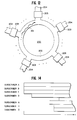
- Fig. 13 shows a memory device with further details regarding portal selection.
- This embodiment is again an example of a memory device 300 provided with a plurality of fixed access portals 301-305 and with a capability of storing a moving data stream. Data can be placed into the device 300 or copied out, as required. The present discussion will focus on data output.
- the internal portals 301-305 are connected to a controller 310, with each portal 301-305 being associated with one input 311-314 to the controller 310.
- the controller 310 provides the selection and switching operability required to output the stored data stream to external signal lines, via output points 351-352.
- logic circuitry including AND gates 321-328 and OR gates 331-332, connects the controller inputs 311-314 to the controller output points 351-352.
- Each AND gate 321-328 has a first input originating at the input 311-314 and a second input constituting a selection line from one of a group of selectors 341-348. Further, each AND gate 321-328 has one output line that forms an input into one of the OR gates 331-332.
- each OR gate 331-332 receives inputs from a number of AND gates 321-328. The number of AND gates 321-328 and the number of OR gates 331-332 is determined by the number of desired controller inputs 311-314 and desired controller output points 351-352, as shown.
- a signal from a given selector e.g., 341 triggers a corresponding AND gate 321.
- the activated AND gate 321 then permits the data stream from its associated output portal 301 to pass through.
- the selection signal 341 is chosen to synchronize with the circulating data stream.
- the portal is selected to be able to "capture” the data stream from its beginning. (If title playback is to commence from some other point, e.g., after a pause operation, the portal is again selected accordingly to "capture” the data stream from the other point.)
- the data stream flows out from the portal 301 and through the appropriate AND gate 321.
- the data stream then appears at the corresponding input to one of the OR gates 331, where it is passed through to the controller output point 351.
- a second selection signal can prompt a second output operation.
- a second AND gate 325 that is connected to the same portal 301 as the one activated in the first output operation is triggered by a further selection signal 345 to forward the data stream.
- a second AND gate e.g., 327
- a selection signal e.g., 347.
- the choice of the AND gate 327 and the portal 303 is determined by the momentary location of the starting point of the data stream in the ring 300.
- Fig. 14 illustrates one output scenario. As shown, requests from subscribers A, B and C give rise to simultaneous, completely overlapping, response outputs. Only one output portal, e.g., 301, need be activated to respond to these three requests. The request from subscriber D is somewhat delayed in time, however, so that the appropriate response output is staggered relative to the response for subscribers A, B and C. Thus, the controller 310 selects a different portal in the ring to respond to the request from subscriber D. Requests from additional subscribers X, Y and Z are handled in like manner.
- the various data storage systems disclosed allow a wide assortment of titles (e.g., movies, educational-, entertainment-, consumer-, and business-related information, and any information that can be converted into a stream of data) to be stored and retrieved by a wide audience with great flexibility and minimal contention between users for the titles offered.
- titles e.g., movies, educational-, entertainment-, consumer-, and business-related information, and any information that can be converted into a stream of data
Landscapes
- Engineering & Computer Science (AREA)
- Multimedia (AREA)
- Signal Processing (AREA)
- Microelectronics & Electronic Packaging (AREA)
- Power Engineering (AREA)
- Television Systems (AREA)
- Storage Device Security (AREA)
- Signal Processing For Digital Recording And Reproducing (AREA)
- Compression, Expansion, Code Conversion, And Decoders (AREA)
- Television Signal Processing For Recording (AREA)
- Iron Core Of Rotating Electric Machines (AREA)
- Vehicle Body Suspensions (AREA)
- Valve Device For Special Equipments (AREA)
- Image Input (AREA)
Claims (58)
- Verfahren, das die folgenden Schritte aufweist:Bereitstellen von Daten, die in einem Speicher gespeichert sind, in einer systematischen zyklischen Anordnung;Vorsehen einer Vielzahl von Datenports (3) in einer durch modulare Arithmetik definierten Anordnung;Vorsehen einer sequentiellen, systematischen, zyklischen Relativbewegung zwischen den gespeicherten Daten und den Datenports; undNutzen der Relativbewegung, um eine Speicherstelle der Daten relativ zu den Datenports zu einem gegebenen Zeitpunkt zu bestimmen.
- Verfahren nach Anspruch 1, wobeisämtliche der Vielzahl von Datenports wiederholt auf sämtliche gespeicherten Daten in Übereinstimmung mit der zyklischen Anordnung und der relativen Bewegung treffen.
- Verfahren nach Anspruch 1, wobeider Schritt des Bereitstellens der gespeicherten Daten das Bereitstellen einer systematischen zyklischen Folge von Datenspeicherstellen für die gespeicherten Daten aufweist.
- Verfahren nach Anspruch 1, wobeider Schritt des Bereitstellens der gespeicherten Daten das Bereitstellen einer Vielzahl von systematisch verbundenen Speichereinrichtungen (2) aufweist.
- Verfahren nach Anspruch 4, wobeider Schritt des Bereitstellens einer Vielzahl von Speichereinrichtungen das Anordnen der Vielzahl von Speichereinrichtungen in einer Anordnung, die durch modulare Arithmetik definiert ist, aufweist.
- Verfahren nach Anspruch 5, wobei die Anordnung der Vielzahl von Speichereinrichtungen definiert ist durch:wobei eine Beziehung zwischen aufeinanderfolgenden Speichereinrichtungen definiert ist durch:Si = eine Speichereinrichtung in der Anordnung, undM = die Gesamtzahl der Vielzahl von vorgesehenen Speichereinrichtungen; undSi = eine Speichereinrichtung in der Anordnung,Si+1 = eine nächste Speichereinrichtung relativ zu Si, undf(t) = eine Funktion der Zeit.
- Verfahren nach Anspruch 6, wobei:
- Verfahren nach Anspruch 1, wobei die Anordnung aus einer Vielzahl von Datenports definiert ist durch:wobei eine Beziehung zwischen konsekutiven Datenports definiert ist durch:Pi = ein Datenport in der Anordnung, undM = die Gesamtzahl der Vielzahl der vorgesehenen Ports; undPi = ein Datenport in der Anordnung,Pi+1 = ein nächster Datenport relativ zu Pi, undf(t) = eine Funktion der Zeit.
- Verfahren nach Anspruch 8, wobei:
- Verfahren nach Anspruch 1, wobei:die Datenports (116) festgelegt sind; unddie gespeicherten Daten an den Datenports vorbeibewegt werden.
- Verfahren nach Anspruch 1, wobei:die gespeicherten Daten an festgelegten Stellen sind; unddie Datenports (111) sich von jeweiligen festgelegten Stellen zu anderen jeweiligen festgelegten Stellen bewegen.
- Verfahren nach Anspruch 1, wobei:die gespeicherten Daten auf eine erste vorbestimmte Weise bewegt werden; unddie Datenports (141) auf eine zweite vorbestimmte Weise bewegt werden.
- Verfahren nach Anspruch 1, wobei die Relativbewegung zwischen den gespeicherten Daten und den Datenports kontinuierlich ist.
- Verfahren nach Anspruch 1, wobei die Relativbewegung zwischen den gespeicherten Daten und den Datenports intermittierend ist.
- Verfahren nach Anspruch 1, das weiterhin den folgenden Schritt aufweist:Ausgeben der gespeicherten Daten von wenigstens einem der Vielzahl von Datenports.
- Verfahren nach Anspruch 1, das weiterhin die folgenden Schritte aufweist:Wählen von wenigstens einem der Datenports (3) in Abhängigkeit von der bestimmten Speicherstelle;Ausgeben der Daten an dem gewählten wenigstens einen Datenport; undwobei der Schritt des Ausgebens der Daten folgendes aufweist:Reproduzieren der Daten; undAusgeben der reproduzierten Daten von dem gewählten wenigstens einen Datenport.
- Verfahren nach Anspruch 1, das ferner die folgenden Schritte aufweist:Wählen eines ersten der Datenports zu einem ersten Zeitpunkt in Abhängigkeit von der bestimmten Speicherstelle;Ausgeben der Daten über den ersten Datenport zu einem ersten Ziel;Nutzen der Relativbewegung, um eine neue Speicherstelle der Daten relativ zu den Datenports zu einem anschließenden Zeitpunkt zu bestimmen;Wählen eines zweiten der Datenports zu einem zweiten Zeitpunkt, der von dem ersten Zeitpunkt verschieden ist, in Abhängigkeit von der neuen bestimmten Speicherstelle; undAusgeben der Daten über den zweiten Datenport zu einem zweiten Ziel.
- Verfahren nach Anspruch 1, wobei der Schritt des Bereitstellens von in einem Speicher gespeicherten Daten folgendes aufweist:Wählen wenigstens eines der Datenports in Abhängigkeit von der bestimmten Speicherstelle; undEingeben von Daten in den Speicher über den wenigstens einen Datenport als die gespeicherten Daten.
- Verfahren nach Anspruch 17, wobei die gewählten Datenports unabhängig voneinander in Abhängigkeit von jeweiligen unabhängigen Wählsignalen gewählt werden.
- Verfahren nach Anspruch 1, das ferner die folgenden Schritte aufweist:Wählen von wenigstens einem der Datenports in Abhängigkeit von der bestimmten Speicherstelle und Abgeben der Daten an dem gewählten wenigstens einen Datenport in Abhängigkeit von der relativen zyklischen Bewegung an eine Telekommunikationsleitung; undÜbertragen der Daten an eine entfernte Station über die Telekommunikationsleitung.
- Verfahren nach Anspruch 1, das ferner die folgenden Schritte aufweist:Wählen von einem Datenport unter der Vielzahl von Datenports in Abhängigkeit von der bestimmten Speicherstelle; undAusgeben der Daten aus dem Speicher über den einen gewählten Datenport zu einer Vielzahl von Abgabezielen.
- Verfahren zum Zugreifen auf Informationen, die in Datenspeicherstellen gehalten werden, wobei das Verfahren die folgenden Schritte aufweist:Bereitstellen einer systematischen Anordnung von einer Vielzahl von Datenspeicherstellen (100);Bereitstellen einer Vielzahl von Datenports (101), die auf eine durch modulare Arithmetik definierte Weise angeordnet sind;Herstellen einer systematischen, relativen, zyklischen Bewegung zwischen den Datenspeicherstellen und den Datenports;Errechnen einer momentanen Speicherstelle innerhalb der Datenspeicherstellen eines gegebenen Teils der Informationen; undWählen eines der Datenports auf der Basis der errechneten momentanen Speicherstelle und Zugreifen auf die Informationen, die in den Datenspeicherstellen gehalten werden, über den gewählten Port in Abhängigkeit von der relativen zyklischen Bewegung.
- Verfahren nach Anspruch 22, wobei der gegebene Teil ein führender Bereich der Informationen ist.
- Verfahren nach Anspruch 22, wobei die momentane Speicherstelle eine aktuelle Speicherstelle ist.
- Verfahren, das die folgenden Schritte aufweist:Bereitstellen eines Datenspeichers (1) zum Speichern von Daten in einer systematischen zyklischen Anordnung;Bereitstellen einer systematischen Anordnung einer Vielzahl von Datenausgängen (3);Bereitstellen einer sequentiellen, systematischen und zyklischen Relativbewegung zwischen den gespeicherten Daten und den Datenausgängen;Wählen eines der Datenausgänge in Abhängigkeit von einem Wählsignal und einer Datenspeicherstellenberechnung, die auf der Relativbewegung basiert; undAusgeben wenigstens eines Segments der gespeicherten Daten von dem gewählten Datenausgang zu einer von einer Vielzahl von Telekommunikationsleitungen.
- Verfahren nach Anspruch 25, wobeider Schritt des Vorsehens von Datenspeichern das Bereitstellen von gespeicherten Daten aufweist.
- Verfahren nach Anspruch 25, wobeider Schritt des Vorsehens von Datenspeichern das Bereitstellen von Datenspeicherstellen aufweist.
- Verfahren nach Anspruch 25, wobei:der Wählschritt zu einem ersten Zeitpunkt durchgeführt wird, um die Daten über den gewählten Datenausgang als einem ersten Datenausgang abzugeben, unddas Verfahren ferner die folgenden Schritte aufweist:Wählen eines zweiten der Datenausgänge zu einem zweiten Zeitpunkt in Abhängigkeit von einem weiteren Wählsignal und einer weiteren Datenspeicherstellenberechnung auf der Basis der Relativbewegung; undAusgeben wenigstens eines Segments der gespeicherten Daten von dem zweiten gewählten Datenausgang an eine zweite der Vielzahl von Telekommunikationsleitungen.
- Verfahren nach Anspruch 25, das ferner den folgenden Schritt aufweist:Ausgeben von wenigstens dem Segment der gespeicherten Daten von dem gewählten Datenausgang an zusätzliche Telekommunikationsleitungen.
- Speichervorrichtung, die folgendes aufweist:eine Datenspeichereinheit (1) zum Speichern von Daten in einer systematischen Anordnung;eine systematische Anordnung aus einer Vielzahl von Datenports (3), die mit der Datenspeichereinheit verbunden sind;eine Einrichtung zum Erzeugen einer relativen, systematischen, zyklischen Bewegung zwischen den in der Datenspeichereinheit gespeicherten Daten und den Datenports; undeine Einrichtung zum Bestimmen einer Speicherstelle der Daten relativ zu den Datenports zu einem gegebenen Zeitpunkt auf der Basis der Bewegung zwischen den Daten und den Datenports.
- Speichervorrichtung nach Anspruch 30, wobei:die Vielzahl von Datenports (3) auf eine durch modulare Arithmetik definierte Weise angeordnet ist.
- Speichervorrichtung nach Anspruch 31, wobei:die Datenspeichereinheit eine Vielzahl von systematisch verbundenen Speichereinrichtungen (2) aufweist.
- Speichervorrichtung nach Anspruch 32, wobei:die Speichereinrichtungen in der Datenspeichereinheit zur Bildung einer Datenspeicherschleife angeordnet sind.
- Speichervorrichtung nach Anspruch 32, wobei:die Speichereinrichtungen in der Datenspeichereinheit zur Bildung eines Rings angeordnet sind.
- Speichervorrichtung nach Anspruch 32, wobei:die Speichereinrichtungen miteinander in Reihe verbunden sind.
- Speichervorrichtung nach Anspruch 32, wobei:die Speichereinrichtungen aus der Gruppe ausgewählt sind, die aus Schieberegistern, statischen Direktzugriffsspeichern, dynamischen Direktzugriffsspeichern, pseudostatischen Direktzugriffsspeichern, Verzögerungsleitungen, Ladungsspeicherbausteinen, Festwertspeichern, programmierbaren Festwertspeichern und nichtflüchtigen Speichern besteht.
- Speichervorrichtung nach Anspruch 32, wobei:wenigstens ein Teil der Einrichtungen mit den genannten Datenports versehen ist.
- Speichervorrichtung nach Anspruch 32, wobei:wenigstens ein Teil der Datenports jeweils zwischen die Speichereinrichtungen in der Datenspeichereinheit eingefügt ist.
- Speichervorrichtung nach Anspruch 31, wobei:die Datenports wenigstens einen Datenkopierer aufweisen.
- Speichervorrichtung nach Anspruch 31, wobei die Datenports (153) physische Speicherplätze sind.
- Speichervorrichtung nach Anspruch 31, wobei wenigstens einige der Datenports aus der Gruppe ausgewählt sind, die aus Zwischenspeichern, Logikgliedern, Regeneratoren und Verstärkern besteht.
- Speichervorrichtung nach Anspruch 31, wobei die Datenports (190) logische Speicherplätze sind.
- Speichervorrichtung nach Anspruch 31, wobei die Mittel zum Ausbilden einer Relativbewegung einen Taktgeber (152) aufweisen.
- Speichervorrichtung nach Anspruch 43, wobei der Taktgeber Datenverschiebeschaltkreise aufweist.
- Speichervorrichtung nach Anspruch 43, wobei der Taktgeber Portverschiebeschaltkreise aufweist.
- Speichervorrichtung nach Anspruch 31, wobei die Mittel zum Ausbilden einer Relativbewegung aus der Gruppe ausgewählt sind, die aus n-Phase-Taktgebern, Taktimpulsgeneratoren, Adreßgeneratoren, Datenmultiplexern und einem Mikroprozessor ausgewählt sind.
- Speichervorrichtung nach Anspruch 31, die ferner folgendes aufweist:eine Steuerungseinheit (6), die mit der Vielzahl von Datenports verbunden und konfiguriert ist, um den Datenverkehr an diesen Datenports zu steuern.
- Speichervorrichtung nach Anspruch 31, die ferner folgendes aufweist:eine Steuerungseinheit (6), die konfiguriert ist, um eine Verbindung zwischen den Datenports und wenigstens einer Ausgangsleitung aufzubauen.
- Speichervorrichtung nach Anspruch 31, die ferner folgendes aufweist:eine Steuerungseinheit (6), die konfiguriert ist, um eine Verbindung zwischen den Datenports und wenigstens einer Eingangsleitung aufzubauen.
- Speichervorrichtung nach Anspruch 31, die ferner folgendes aufweist:eine Steuerungseinheit (6), die konfiguriert ist, um unter den Datenports in Abhängigkeit von einem von der Bestimmungseinrichtung abgegebenen Wählsignal (8) eine Wahl zu treffen.
- Speichervorrichtung nach Anspruch 31, die ferner folgendes aufweist:eine Steuerungseinheit, die konfiguriert ist, um unter der Vielzahl von Datenports einen Datenport zu wählen und die Daten über den einen gewählten Datenport an eine Vielzahl von Abgabezielen abzugeben.
- Speichervorrichtung, die folgendes aufweist:eine Datenspeichereinheit, die eine systematische Anordnung von Datenspeicherstellen zum Speichern von Daten hat;eine Vielzahl von Datenports, die mit den Datenspeicherstellen verbunden und auf eine Weise, die durch modulare Arithmetik definiert ist, angeordnet sind;einen Generator, der konfiguriert ist zur Ausbildung einer relativen, systematischen, zyklischen Bewegung zwischen den Datenspeicherstellen und den Datenports; undeine Steuerungseinheit, die konfiguriert ist zur Wahl eines Datenports unter der Vielzahl von Datenports in Abhängigkeit von einer Datenspeicherstellenrechnung, die auf der Relativbewegung basiert, und zum Verbinden des gewählten einen Datenports mit einer von einer Vielzahl von Fernmeldeleitungen, die mit der Speichervorrichtung verbunden sind.
- Speichervorrichtung, die folgendes aufweist:ein Speichermedium (200) zur Aufnahme von zyklisch sich ausbreitenden Daten (201); undeine systematische Anordnung einer Mehrzahl von Datenports (203), die mit dem Speichermedium auf solche Weise verbunden sind, daß die Datenports wiederholt auf die sich zyklisch ausbreitenden Daten treffen; undeine Einrichtung zum Bestimmen einer momentanen Speicherstelle der sich zyklisch ausbreitenden Daten auf der Basis einer Ausbreitungsrate der Daten.
- Speichervorrichtung nach Anspruch 53, wobei wenigstens einige der Datenports Datenausgänge sind, die ausgebildet sind, um die sich ausbreitenden Daten zu kopieren.
- Speichervorrichtung nach Anspruch 53, wobei:die Vielzahl von Datenports (203) um das Speichermedium herum auf eine durch modulare Arithmetik definierte Weise angeordnet ist.
- Speichervorrichtung nach Anspruch 55, wobei das Speichermedium aus der Gruppe ausgewählt ist, die besteht aus: elektrischem Kabel, Koaxialkabel, Nachhall-Leitungen, Verzögerungsleitungen, Lichtwellenleiterkabel und Mikrowellen-Hohlraumresonatoren.
- Speichervorrichtung nach Anspruch 55, wobei wenigstens einige der Datenports konfiguriert sind, um die sich ausbreitenden Daten anzuzapfen.
- Speichervorrichtung nach Anspruch 55, wobei wenigstens einige der Datenports aus der Gruppe ausgewählt sind, die besteht aus: Verstärkern, Regeneratoren, Strahlteilern, Mikrowellen-Hohlraumresonator-Abgriffen und Koaxialkabel-Abgriffen.
Applications Claiming Priority (3)
| Application Number | Priority Date | Filing Date | Title |
|---|---|---|---|
| US249265 | 1994-05-25 | ||
| US08/249,265 US6356973B1 (en) | 1993-10-15 | 1994-05-25 | Memory device having a cyclically configured data memory and having plural data portals for outputting/inputting data |
| PCT/US1995/006139 WO1995032505A1 (en) | 1994-05-25 | 1995-05-19 | Memory device |
Publications (2)
| Publication Number | Publication Date |
|---|---|
| EP0763243A1 EP0763243A1 (de) | 1997-03-19 |
| EP0763243B1 true EP0763243B1 (de) | 1998-10-28 |
Family
ID=22942722
Family Applications (1)
| Application Number | Title | Priority Date | Filing Date |
|---|---|---|---|
| EP95920463A Expired - Lifetime EP0763243B1 (de) | 1994-05-25 | 1995-05-19 | Speichereinrichtung |
Country Status (6)
| Country | Link |
|---|---|
| US (2) | US6356973B1 (de) |
| EP (1) | EP0763243B1 (de) |
| AU (1) | AU711519B2 (de) |
| CA (1) | CA2191113A1 (de) |
| DE (1) | DE69505661T2 (de) |
| WO (1) | WO1995032505A1 (de) |
Families Citing this family (16)
| Publication number | Priority date | Publication date | Assignee | Title |
|---|---|---|---|---|
| US7003168B1 (en) * | 1997-03-11 | 2006-02-21 | Vianet Technologies, Inc. | Image compression and decompression based on an integer wavelet transform using a lifting scheme and a correction method |
| US6567417B2 (en) * | 2000-06-19 | 2003-05-20 | Broadcom Corporation | Frame forwarding in a switch fabric |
| US6879526B2 (en) * | 2002-10-31 | 2005-04-12 | Ring Technology Enterprises Llc | Methods and apparatus for improved memory access |
| US7707351B2 (en) * | 2002-10-31 | 2010-04-27 | Ring Technology Enterprises Of Texas, Llc | Methods and systems for an identifier-based memory section |
| US7197662B2 (en) * | 2002-10-31 | 2007-03-27 | Ring Technology Enterprises, Llc | Methods and systems for a storage system |
| US7415565B2 (en) * | 2002-10-31 | 2008-08-19 | Ring Technology Enterprises, Llc | Methods and systems for a storage system with a program-controlled switch for routing data |
| ATE449411T1 (de) * | 2003-03-14 | 2009-12-15 | Nxp Bv | Zweidimensionaler datenspeicher |
| US7401179B2 (en) * | 2005-01-21 | 2008-07-15 | Infineon Technologies Ag | Integrated circuit including a memory having low initial latency |
| US7634622B1 (en) | 2005-06-14 | 2009-12-15 | Consentry Networks, Inc. | Packet processor that generates packet-start offsets to immediately store incoming streamed packets using parallel, staggered round-robin arbitration to interleaved banks of memory |
| US7577868B2 (en) * | 2005-09-30 | 2009-08-18 | Lockheed Martin Corporation | No data loss IT disaster recovery over extended distances |
| US7742335B2 (en) | 2007-10-31 | 2010-06-22 | Micron Technology, Inc. | Non-volatile multilevel memory cells |
| US7848142B2 (en) * | 2007-10-31 | 2010-12-07 | Micron Technology, Inc. | Fractional bits in memory cells |
| JP6115308B2 (ja) * | 2013-05-22 | 2017-04-19 | 富士通株式会社 | 情報処理システム、情報処理システムの制御方法、及び制御プログラム |
| GB2523165B (en) * | 2014-02-17 | 2018-09-26 | Technetix Bv | Cable television cable tap device |
| US10313641B2 (en) * | 2015-12-04 | 2019-06-04 | Google Llc | Shift register with reduced wiring complexity |
| JP6902000B2 (ja) * | 2018-07-10 | 2021-07-14 | 株式会社東芝 | 演算装置 |
Citations (2)
| Publication number | Priority date | Publication date | Assignee | Title |
|---|---|---|---|---|
| US4193121A (en) * | 1976-07-16 | 1980-03-11 | Post Office | Information handling apparatus having multiple ports distributed around shifting register rings |
| EP0596656A2 (de) * | 1992-11-05 | 1994-05-11 | AT&T Corp. | Programmierbare Schaltung zur Anpassung einer Taktverschiebung |
Family Cites Families (21)
| Publication number | Priority date | Publication date | Assignee | Title |
|---|---|---|---|---|
| US3713096A (en) | 1971-03-31 | 1973-01-23 | Ibm | Shift register interconnection of data processing system |
| US3748647A (en) | 1971-06-30 | 1973-07-24 | Ibm | Toroidal interconnection system |
| US3735362A (en) | 1971-09-22 | 1973-05-22 | Ibm | Shift register interconnection system |
| US3812476A (en) | 1971-11-16 | 1974-05-21 | Texas Instruments Inc | Memory device |
| US4064556A (en) | 1975-06-23 | 1977-12-20 | Sperry Rand Corporation | Packed loop memory with data manipulation capabilities |
| US4065756A (en) | 1976-03-15 | 1977-12-27 | Burroughs Corporation | Associative memory with neighboring recirculated paths offset by one bit |
| IT1118355B (it) | 1979-02-15 | 1986-02-24 | Cselt Centro Studi Lab Telecom | Sistema di interconnessione tra processori |
| US4363125A (en) | 1979-12-26 | 1982-12-07 | International Business Machines Corporation | Memory readback check method and apparatus |
| US4506387A (en) | 1983-05-25 | 1985-03-19 | Walter Howard F | Programming-on-demand cable system and method |
| US4792848A (en) | 1986-12-02 | 1988-12-20 | Scientific-Atlanta, Inc. | Cable television impulse pay per view system |
| US4829372A (en) | 1987-08-20 | 1989-05-09 | Telaction Corporation | Presentation player |
| US5119481A (en) | 1987-12-22 | 1992-06-02 | Kendall Square Research Corporation | Register bus multiprocessor system with shift |
| US4975605A (en) * | 1989-11-13 | 1990-12-04 | Intel Corporation | Synchronous delay line with automatic reset |
| US5084839A (en) | 1990-02-05 | 1992-01-28 | Harris Corporation | Variable length shift register |
| US5093718A (en) | 1990-09-28 | 1992-03-03 | Inteletext Systems, Inc. | Interactive home information system |
| US5526034A (en) | 1990-09-28 | 1996-06-11 | Ictv, Inc. | Interactive home information system with signal assignment |
| US5357276A (en) | 1992-12-01 | 1994-10-18 | Scientific-Atlanta, Inc. | Method of providing video on demand with VCR like functions |
| EP0609054A3 (en) | 1993-01-25 | 1996-04-03 | Matsushita Electric Industrial Co Ltd | Method and apparatus for recording or reproducing video data on or from storage media. |
| US5440334A (en) | 1993-02-01 | 1995-08-08 | Explore Technology, Inc. | Broadcast video burst transmission cyclic distribution apparatus and method |
| US5414455A (en) | 1993-07-07 | 1995-05-09 | Digital Equipment Corporation | Segmented video on demand system |
| US5477263A (en) | 1994-05-26 | 1995-12-19 | Bell Atlantic Network Services, Inc. | Method and apparatus for video on demand with fast forward, reverse and channel pause |
-
1994
- 1994-05-25 US US08/249,265 patent/US6356973B1/en not_active Expired - Fee Related
-
1995
- 1995-05-19 AU AU26070/95A patent/AU711519B2/en not_active Ceased
- 1995-05-19 CA CA002191113A patent/CA2191113A1/en not_active Abandoned
- 1995-05-19 EP EP95920463A patent/EP0763243B1/de not_active Expired - Lifetime
- 1995-05-19 DE DE69505661T patent/DE69505661T2/de not_active Expired - Lifetime
- 1995-05-19 WO PCT/US1995/006139 patent/WO1995032505A1/en not_active Ceased
-
2001
- 2001-12-11 US US10/011,775 patent/US6779073B2/en not_active Expired - Fee Related
Patent Citations (2)
| Publication number | Priority date | Publication date | Assignee | Title |
|---|---|---|---|---|
| US4193121A (en) * | 1976-07-16 | 1980-03-11 | Post Office | Information handling apparatus having multiple ports distributed around shifting register rings |
| EP0596656A2 (de) * | 1992-11-05 | 1994-05-11 | AT&T Corp. | Programmierbare Schaltung zur Anpassung einer Taktverschiebung |
Non-Patent Citations (2)
| Title |
|---|
| 'HANDBUCH DER MAGNETSPEICHERTECHNIK', C. SCHOLZ, HANSER VERLAG, MüNCHEN, 1980 * |
| W.D. SINCOSKIE: "SYSTEM ARCHITECTURE FOR A LARGE SCALE VIDEO ON DEMAND SERVICE", COMPUTER NETWORKS AND ISDN SYSTEMS, vol. 22, 1991, NORTH HOLLAND, pages 155 - 162, XP026648228, DOI: doi:10.1016/0169-7552(91)90007-Y * |
Also Published As
| Publication number | Publication date |
|---|---|
| US6779073B2 (en) | 2004-08-17 |
| US20020062420A1 (en) | 2002-05-23 |
| DE69505661T2 (de) | 1999-07-08 |
| EP0763243A1 (de) | 1997-03-19 |
| AU2607095A (en) | 1995-12-18 |
| AU711519B2 (en) | 1999-10-14 |
| CA2191113A1 (en) | 1995-11-30 |
| WO1995032505A1 (en) | 1995-11-30 |
| US6356973B1 (en) | 2002-03-12 |
| DE69505661D1 (de) | 1998-12-03 |
Similar Documents
| Publication | Publication Date | Title |
|---|---|---|
| EP0763243B1 (de) | Speichereinrichtung | |
| EP0697703B1 (de) | Videospeicher-Gerät und -Verfahren | |
| EP0707423B1 (de) | Videosignalwiedergabeeinrichtung | |
| KR100293856B1 (ko) | 인터액티브텔레비젼시스템용프로그램서버 | |
| EP0686908B1 (de) | Datenanbieter für Video-auf-Abruf-System | |
| EP0804028B1 (de) | Video-auf-anfragesystem mit verzögerung und fernsehverfahren dazu | |
| EP0723731B1 (de) | Stelle zur steuerung von informationsdiensten | |
| US6185621B1 (en) | Direct copying between disk blocks in memory onto a network as sequential access files | |
| MX9801217A (es) | Un metodo y un aparato para codificar una corriente de bits por la conexion de multiples angulos. | |
| GB2287845A (en) | Multichannel Video Data Storage | |
| JPH11509993A (ja) | インフォメーションオンディマンドシステム | |
| JPH11509951A (ja) | 記憶媒体装置 | |
| US6792196B1 (en) | Reproduction method and reproduction apparatus | |
| US6144796A (en) | Video data system | |
| EP0975164B1 (de) | Bildermittlungssystem- und Verfahren | |
| US6003071A (en) | Image data transmission apparatus using time slots | |
| KR19980703631A (ko) | 정보 서비스 시스템 | |
| EP0743790B1 (de) | Gerät zur Übertragung von Bilddaten | |
| JP3401978B2 (ja) | オーディオ・ビデオ信号提供装置 | |
| JP4325073B2 (ja) | データ記録再生装置及び方法 | |
| JPH08317341A (ja) | データ送出方法 | |
| JP2003284033A (ja) | ニアビデオオンデマンド装置 | |
| HK1007934B (en) | Program server for an interactive television system |
Legal Events
| Date | Code | Title | Description |
|---|---|---|---|
| PUAI | Public reference made under article 153(3) epc to a published international application that has entered the european phase |
Free format text: ORIGINAL CODE: 0009012 |
|
| 17P | Request for examination filed |
Effective date: 19961211 |
|
| AK | Designated contracting states |
Kind code of ref document: A1 Designated state(s): CH DE FR GB IE IT LI |
|
| 17Q | First examination report despatched |
Effective date: 19970808 |
|
| GRAG | Despatch of communication of intention to grant |
Free format text: ORIGINAL CODE: EPIDOS AGRA |
|
| GRAG | Despatch of communication of intention to grant |
Free format text: ORIGINAL CODE: EPIDOS AGRA |
|
| GRAH | Despatch of communication of intention to grant a patent |
Free format text: ORIGINAL CODE: EPIDOS IGRA |
|
| GRAH | Despatch of communication of intention to grant a patent |
Free format text: ORIGINAL CODE: EPIDOS IGRA |
|
| GRAA | (expected) grant |
Free format text: ORIGINAL CODE: 0009210 |
|
| AK | Designated contracting states |
Kind code of ref document: B1 Designated state(s): CH DE FR GB IE IT LI |
|
| REG | Reference to a national code |
Ref country code: CH Ref legal event code: EP |
|
| REF | Corresponds to: |
Ref document number: 69505661 Country of ref document: DE Date of ref document: 19981203 |
|
| REG | Reference to a national code |
Ref country code: IE Ref legal event code: FG4D |
|
| ITF | It: translation for a ep patent filed | ||
| ET | Fr: translation filed | ||
| REG | Reference to a national code |
Ref country code: CH Ref legal event code: NV Representative=s name: ISLER & PEDRAZZINI AG |
|
| PLBE | No opposition filed within time limit |
Free format text: ORIGINAL CODE: 0009261 |
|
| STAA | Information on the status of an ep patent application or granted ep patent |
Free format text: STATUS: NO OPPOSITION FILED WITHIN TIME LIMIT |
|
| 26N | No opposition filed | ||
| REG | Reference to a national code |
Ref country code: GB Ref legal event code: IF02 |
|
| PGFP | Annual fee paid to national office [announced via postgrant information from national office to epo] |
Ref country code: IE Payment date: 20060526 Year of fee payment: 12 |
|
| PGFP | Annual fee paid to national office [announced via postgrant information from national office to epo] |
Ref country code: CH Payment date: 20060530 Year of fee payment: 12 |
|
| REG | Reference to a national code |
Ref country code: CH Ref legal event code: PCAR Free format text: ISLER & PEDRAZZINI AG;POSTFACH 1772;8027 ZUERICH (CH) |
|
| REG | Reference to a national code |
Ref country code: CH Ref legal event code: PL |
|
| REG | Reference to a national code |
Ref country code: IE Ref legal event code: MM4A |
|
| PG25 | Lapsed in a contracting state [announced via postgrant information from national office to epo] |
Ref country code: LI Free format text: LAPSE BECAUSE OF NON-PAYMENT OF DUE FEES Effective date: 20070531 Ref country code: CH Free format text: LAPSE BECAUSE OF NON-PAYMENT OF DUE FEES Effective date: 20070531 |
|
| PG25 | Lapsed in a contracting state [announced via postgrant information from national office to epo] |
Ref country code: IE Free format text: LAPSE BECAUSE OF NON-PAYMENT OF DUE FEES Effective date: 20070521 |
|
| PG25 | Lapsed in a contracting state [announced via postgrant information from national office to epo] |
Ref country code: IT Free format text: LAPSE BECAUSE OF NON-PAYMENT OF DUE FEES Effective date: 20070519 |
|
| PGRI | Patent reinstated in contracting state [announced from national office to epo] |
Ref country code: IT Effective date: 20091001 |
|
| PGFP | Annual fee paid to national office [announced via postgrant information from national office to epo] |
Ref country code: IT Payment date: 20090812 Year of fee payment: 13 |
|
| PGFP | Annual fee paid to national office [announced via postgrant information from national office to epo] |
Ref country code: FR Payment date: 20100525 Year of fee payment: 16 |
|
| PGFP | Annual fee paid to national office [announced via postgrant information from national office to epo] |
Ref country code: DE Payment date: 20100531 Year of fee payment: 16 |
|
| PGFP | Annual fee paid to national office [announced via postgrant information from national office to epo] |
Ref country code: GB Payment date: 20100401 Year of fee payment: 16 |
|
| REG | Reference to a national code |
Ref country code: DE Ref legal event code: R119 Ref document number: 69505661 Country of ref document: DE |
|
| REG | Reference to a national code |
Ref country code: DE Ref legal event code: R119 Ref document number: 69505661 Country of ref document: DE |
|
| GBPC | Gb: european patent ceased through non-payment of renewal fee |
Effective date: 20110519 |
|
| REG | Reference to a national code |
Ref country code: FR Ref legal event code: ST Effective date: 20120131 |
|
| PG25 | Lapsed in a contracting state [announced via postgrant information from national office to epo] |
Ref country code: FR Free format text: LAPSE BECAUSE OF NON-PAYMENT OF DUE FEES Effective date: 20110531 |
|
| PG25 | Lapsed in a contracting state [announced via postgrant information from national office to epo] |
Ref country code: GB Free format text: LAPSE BECAUSE OF NON-PAYMENT OF DUE FEES Effective date: 20110519 |
|
| PG25 | Lapsed in a contracting state [announced via postgrant information from national office to epo] |
Ref country code: DE Free format text: LAPSE BECAUSE OF NON-PAYMENT OF DUE FEES Effective date: 20111130 |
|
| PGRI | Patent reinstated in contracting state [announced from national office to epo] |
Ref country code: IT Effective date: 20091001 |