EP0757433B1 - Vorrichtung und Verfahren zur Frequenzregelung eines PLL-Demodulators - Google Patents
Vorrichtung und Verfahren zur Frequenzregelung eines PLL-Demodulators Download PDFInfo
- Publication number
- EP0757433B1 EP0757433B1 EP96401701A EP96401701A EP0757433B1 EP 0757433 B1 EP0757433 B1 EP 0757433B1 EP 96401701 A EP96401701 A EP 96401701A EP 96401701 A EP96401701 A EP 96401701A EP 0757433 B1 EP0757433 B1 EP 0757433B1
- Authority
- EP
- European Patent Office
- Prior art keywords
- frequency
- signal
- value
- voltage controlled
- controlled oscillator
- Prior art date
- Legal status (The legal status is an assumption and is not a legal conclusion. Google has not performed a legal analysis and makes no representation as to the accuracy of the status listed.)
- Expired - Lifetime
Links
Images


Classifications
-
- H—ELECTRICITY
- H03—ELECTRONIC CIRCUITRY
- H03D—DEMODULATION OR TRANSFERENCE OF MODULATION FROM ONE CARRIER TO ANOTHER
- H03D3/00—Demodulation of angle-, frequency- or phase- modulated oscillations
- H03D3/02—Demodulation of angle-, frequency- or phase- modulated oscillations by detecting phase difference between two signals obtained from input signal
- H03D3/24—Modifications of demodulators to reject or remove amplitude variations by means of locked-in oscillator circuits
- H03D3/241—Modifications of demodulators to reject or remove amplitude variations by means of locked-in oscillator circuits the oscillator being part of a phase locked loop
- H03D3/244—Modifications of demodulators to reject or remove amplitude variations by means of locked-in oscillator circuits the oscillator being part of a phase locked loop combined with means for obtaining automatic gain control
Definitions
- the present invention relates to an apparatus and method for setting up a tuning frequency of a phase-locked loop demodulator.
- the present invention compensates for dispersion and aging effects of a resonating frequency of an associated ceramic resonator.
- the present invention is applicable to systems that receive a plurality of carrier frequencies and is particularly applicable to sound demodulation that is associated with analog satellite receivers.
- Fig. 1 illustrates a basic block diagram of a circuit that is used to set up the tuning frequency of a phase-locked loop demodulator.
- the phase-locked loop demodulator 100 includes: a voltage controlled oscillator (VCO) 110; a phase detector 120; a low pass filter 130 (LPF); and a programmable attenuator 140.
- VCO voltage controlled oscillator
- LPF low pass filter 130
- the circuit for setting up the tuning frequency of the phase-locked loop (PLL) demodulator 100 includes: first and second switches S1, S2 that are respectively controlled by anti-phase signals CS and NCS; a capacitor 145; a frequency synthesizing circuit 150; a frequency comparator 160; a reference frequency generator 170; and a control circuit 180.
- the demodulation approach adopted with this circuit is direct. That is to say, the signal demodulation is performed directly at the sub-carrier frequency, i.e., there is no frequency shift.
- the VCO 110 of the PLL demodulator 100 is controlled by the frequency synthesizing circuit 150.
- the adjustable attenuator 140 provides the required control of the PLL demodulators gain, i.e., the lock and capture ranges. Such precision is necessary so as to avoid locking onto an undesired adjacent subcarrier and to be compatible with different deviations in the subcarriers.
- EP-A-0 645 881, EP-A-0 645 882 and EP-A-0 645 891 which are all assigned to SGS-THOMSON Microelectronics Ltd., describe in more detail the structure and operation of the basic block diagram of Fig. 1.
- Fig. 2 illustrates a basic block diagram of the frequency synthesizing circuit 150.
- the frequency synthesizing circuit 150 includes: a programmable frequency divider 200, a phase comparator 210 for comparing the frequency signals fDIV and fREF that are respectively supplied by the programmable frequency divider 200 and the reference frequency generator 170; and a controlled current source/sink circuit IS1, IS2, S3, S4 for sourcing and sinking current to and from the input of the VCO via switch S2.
- Switches S3 and S4 are operatively controlled by outputs of the phase comparator 210. With successive charges and discharges through switch S2, the voltage across the capacitor 145 reaches the required value so as to operatively control the VCO.
- EP-A-0 645 881 and EP-A-0 645 891 describe in more detail the structure and operation of the basic block diagram of Fig. 2.
- the reference frequency generator 170 illustrated in Figs. 1 and 2 is normally provided by an oscillator circuit that includes a piezoelectric crystal.
- quartz crystals can be manufactured such that their resonant frequencies are very accurate. Furthermore, it is possible to very accurately control the dispersion between one quartz crystal and another, or in other words, the manufacturing tolerances that can be attained for a series of quartz crystals can be extremely high.
- the frequency tolerance from one crystal to another varies by approximately 0.001% and the frequency stability by approximately 0.01%, where frequency stability is defined as the frequency tolerance over an operating temperature range with respect to a frequency at a reference temperature. Also, even though the long-term stability of a crystal is affected by a number of complex factors, its variation over a ten year period for example will be typically 0.001%.
- An object of the present invention is to provide an alternative cost effective solution to that of a piezoelectric crystal.
- Another object of the present invention is to provide an alternative solution to a piezoelectric crystal that provides a reasonable frequency tolerance and reasonable long-term and short-term frequency stability.
- Another object of the present invention is to replace the piezoelectric crystal with a less expensive ceramic resonator.
- Another object of the present invention is to compensate for any changes in the frequency tolerance and long term or short term stability of a ceramic resonator.
- the present invention proposes an apparatus for setting up the tuning frequency of a phase-locked loop demodulator that includes a voltage controlled oscillator and a first switch.
- the apparatus also includes frequency synthesizing circuitry whose output is connected to a second switch.
- the frequency synthesizing circuitry receives an output from the voltage controlled oscillator which is proportional to the frequency of the voltage controlled oscillator and a reference frequency for operatively controlling, via said second switch, the voltage controlled oscillator.
- circuitry for providing a first signal which corresponds to the difference between the output frequency of the voltage controlled oscillator and the reference frequency and circuitry that is responsive to a plurality of signals including the first signal for operatively controlling the apparatus, including selecting the tuning frequency of the frequency synthesizing circuitry.
- the apparatus further includes: a ceramic resonator oscillator in the reference frequency generator for providing the reference frequency; a latch or some other suitable memory circuit for storing the value of the first signal; and comparison and calibration circuitry that is capable of comparing the stored value of the first signal with a current value of the first signal so as to produce a second signal for adjusting the tuning frequency of the frequency synthesizing circuitry in response to the second signal, i.e., for calibrating the tuning frequency of the frequency synthesizing circuitry.
- the calibration means includes a microprocessor and an associated memory, for example a non-volatile E2PROM memory, for storing the value of the first signal.
- the memory may be monolithically integrated along with the microprocessor. Additionally, the memory may be a non-volatile memory.
- the value of the first signal is initially stored as part of a testing procedure during the manufacturing of the apparatus.
- updated values of the first signal can be stored during the operation of the apparatus and/or the power-up or start sequence of the apparatus and/or the power-down or stop sequence of the apparatus.
- the apparatus can be used in satellite signal receiver systems, radio signal receiver systems, television signal receiver systems and video signal receiver systems and any combination of said systems.
- a method for setting up the tuning frequency of a phase-locked loop demodulator that includes a voltage controlled oscillator.
- the method includes the steps of: generating a reference frequency; connecting a frequency synthesizer to the voltage controlled oscillator; synthesizing a tuning frequency for the voltage controlled oscillator that substantially corresponds to a required carrier frequency; generating a first signal that corresponds to the difference between the synthesized tuning frequency and the reference frequency; disconnecting the frequency synthesizer from the voltage controlled oscillator; connecting a plurality of carrier frequencies to the phase-locked loop demodulator; and adjusting the voltage controlled oscillator such that its frequency corresponds to a desired carrier frequency.
- the method further includes the steps of: generating the reference frequency by means of circuitry that includes a ceramic resonator; storing the value of the first signal; comparing the stored value of the first signal with the current value of the first signal; producing a second signal in response to said comparison; applying the second signal to the frequency synthesizer; and adjusting the tuning frequency in response to the second signal.
- the step of memorizing the value of the first signal is initially carried out as part of a testing procedure during the manufacturing process.
- the method further includes the step of updating the memorized value of the first signal during normal operation and/or the power-up or start sequence and/or the power-down or stop sequence.
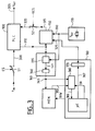
- Fig. 3 illustrates a block diagram of a circuit that is used to set up the tuning frequency of a phase-locked loop demodulator according to an embodiment of the present invention.
- the phase-locked loop demodulator 100 includes the VCO 110, the phase detector 120, the low pass filter 130, and the programmable attenuator 140 as shown in Fig. 1.
- the circuit for setting up the tuning frequency of the PLL demodulator includes, the switches S1 and S2, a frequency synthesizing circuit 450, a frequency comparator 460, a reference frequency generator 470, and a control circuit 480.
- the input terminal 300 to the demodulator 100 receives, via switch S1, the plurality of input carrier signals fIN.
- the output terminal 305 of the demodulator provides the required demodulated output signal VOUT.
- the output terminal 310 of the VCO is received by a frequency synthesizing circuit 450 and a frequency comparator 460.
- the output terminal 315 of the synthesizing circuit 450 is connected to the input terminal 320 of the VCO via switch S2.
- a frequency divider and phase comparator within the synthesizing circuit 450 receive the respective outputs 325 and 330 from a control circuit 480 and a reference frequency generator 470.
- the reference frequency generator 470 uses a ceramic resonator as the basis for generating a reference frequency.
- a piezoelectric crystal is substituted with a ceramic resonator such that the method and circuitry compensate for the relatively large tolerance and stability dispersions associated with a ceramic resonator.
- the frequency tolerance and long-term frequency stability of a typical ceramic resonator are both in the order of approximately +/-0.5% and it is these excessive dispersions that are the root of the problem having contemplated using a ceramic resonator.
- This +/-0.5% frequency tolerance is at the extreme limit of acceptability, especially for industrial mass production and can thus not be relied upon.
- the +/-0.5% long-term frequency stability is, in the case of industrial mass production, totally unacceptable.
- the solution according to an embodiment of the present invention is somewhat convoluted in that a straight substitution of a ceramic resonator for a crystal introduces these tolerance and stability problems. So having solved one non-technical cost related problem, another more serious technical non-cost related problem is created, or in other words, there is a nested problem to the solution of the original problem.
- the embodiment of the present invention overcomes both of the problems that are associated with substituting the piezoelectric crystal with a ceramic resonator.
- the frequency comparator 460 which is similar to that described in the aforementioned STV0042/56 data sheet and referred to as a watchdog, includes a frequency comparator 335 that is capable of measuring and comparing the frequency at the output terminal 310 of the VCO 110 with that at the output terminal 330 of the reference frequency generator 470.
- the result of the comparison is received, via an output 337, by a register 340.
- the register 340 holds, i.e., temporarily stores, the resultant value of the comparison in a suitable format, for example a digital format, that is acceptable to the elements downstream of this register.
- the output 345 of the watchdog register 340 is supplied to a memory circuit MEM.
- the memory circuit MEM is preferably a Read/Write non-volatile type memory, an example being a E2PROM memory, whose read and write cycles are controlled by a R/W control signal that is provided by the control circuit 480.
- the respective outputs 350 and 345 from the memory MEM and the watchdog register 340 are received by comparison circuitry 360.
- This comparison circuitry 360 compares the data, which relates to frequency measurements, and supplies a result, via an output 365, to a microcontroller ⁇ C.
- the microcontroller ⁇ C requests data from the comparison circuit 360 via a control signal DR.
- the microcontroller ⁇ C Based on the result supplied to the microcontroller ⁇ C by the comparison circuit 360, the microcontroller ⁇ C supplies data, via an output 367, to another register 370 that is associated with the frequency synthesizing circuit 450.
- Register 370 is used to hold or latch the data for programming the frequency divider of the frequency synthesizing circuit 450 (see Fig. 2) including the additional data that is required for adjusting the frequency divider should there be any dispersion of the frequency tolerance and/or stability of the ceramic resonator.
- microcontroller ⁇ C can also directly access the data from the watchdog register 340 and the memory MEM and that the outputs 337, 345, 350, 365 and 367 may be data bus type parallel outputs.
- the proposed method can be categorized into two distinct general operations.
- the first operation involves the calibration of a ceramic resonator and indeed its direct and indirect associated circuitry.
- the second operation involves compensating for changes in the tolerance and/or stability of the ceramic resonator.
- the accuracy of the reference frequency derived from a ceramic resonator, is not yet known.
- Step #1 includes respectively opening and closing switches S1 and S2.
- Switch S1 acts to block a plurality of input carrier frequency signals fIN from passing through to the demodulator 100 and switch S2 operatively connects the frequency synthesizer 450 to the VCO 110 of the demodulator 100. It should be noted that switches S1 and S2 are controlled in anti-phase by the respective control signals CS and NCS.
- Step #2 includes driving, i.e., controlling, the VCO 110 by means of the frequency synthesizer 450 so as to obtain an output signal that corresponds to a frequency value of fVCOA, where fVCOA substantially corresponds to a required carrier frequency fo.
- the VCO 110 is driven by the frequency synthesizer 450 which is in turn driven by the reference frequency generator 470 that contains the ceramic resonator.
- the frequency synthesizer 450 is programmed with an arbitrary coefficient NARB for adjusting the frequency synthesizer 450. This arbitrary coefficient NARB could have either a positive, negative or zero value.
- Step #3 includes, having stimulated the VCO 110 to produce an output frequency value equal to fVCOA, comparing the signal fVCOA and the actual reference frequency fREFA. The result of this comparison is held in the register 340 and stored in the non-volatile memory MEM.
- the frequency comparator 460 produces the resultant signal of the comparison between the signals fVCOA and fREFA, which is in the very first instance of the comparison of fVCOA and fREFA, the coefficient NTH which is to be used during the adjustment of the frequency synthesizer 450.
- Step #4 includes, having completed the non-volatile storage of the coefficient NTH, respectively opening and closing switches S1 and S2.
- Switch S1 now acts to pass the plurality of input carrier frequency signals fIN to the demodulator 100, including the required carrier frequency fo.
- Step #5 includes, once the required carrier frequency fo has been captured, comparing it with the actual reference frequency fREFA. Since the running frequency of the VCO 110 has now been changed from fVCOA to fo, the frequency comparator 460 now produces another signal NM as a result of comparing fREFA and fo, i.e., f'VCOA.
- the result of the calibration operation is stored in the non-volatile memory MEM.
- the results NTH and NM can be processed to obtain the result C which is then stored in the memory MEM.
- An advantage of this alternative is that less memory space is required.
- the present invention is susceptible to being carried out as part of a software routine and/or as a hardware solution.
- a phase-locked loop demodulator that has a ceramic resonator as a reference frequency source or generator can be implemented which overcomes the current state of the art problems. Furthermore, the principle of comparing the VCO output frequency with that provided by the ceramic resonator based frequency source, and the storing and operative processing and application of compensation coefficients can be applied to a great number of circuits and applications that currently use piezoelectric crystals as a frequency reference source, provided that such applications include or are adapted to include the necessary elements such as a frequency comparator, a non-volatile memory, and operative control circuitry.
Landscapes
- Engineering & Computer Science (AREA)
- Power Engineering (AREA)
- Stabilization Of Oscillater, Synchronisation, Frequency Synthesizers (AREA)
Claims (16)
- Vorrichtung zum Einstellen der Abstimmfrequenz eines Phase-Locked-Loop-Demodulators (100), der einen spannungsgesteuerten Oszillator (110) und eine erste Schaltvorrichtung (S1) aufweist, wobei die Vorrichtung aufweist:dadurch gekennzeichnet, daßeine frequenzerzeugende Schaltung (150), deren Ausgang (315) an eine zweite Schaltvorrichtung (S2) angeschlossen ist, die einen Ausgang (310) des spannungsgesteuerten Oszillators empfängt, der proportional zu seiner Frequenz und einer Referenzfrequenz (fREF) ist, um im Betrieb den spannungsgesteuerten Oszillator über die zweite Schaltvorrichtung zu steuern,eine Schaltung (160) zum Erzeugen eines ersten Signals, das der Differenz zwischen der Ausgangsfrequenz des spannungsgesteuerten Oszillators und der Referenzfrequenz entspricht,eine Schaltung (180), die auf mehrere Signale und das erste Signal reagiert, um die Vorrichtung im Betrieb zu steuern,
die Apparatur außerdem aufweist:einen Keramikresonatoroszillator zum Erzeugen der Referenzfrequenz;eine Vorrichtung (MEM) zum Speichern des Wertes des ersten Signals; undeine Vergleichsvorrichtung (360) zum Vergleichen des gespeicherten Wertes des ersten Signals mit einem aktuellen Wert des ersten Signals, so daß ein zweites Signal zum Abstimmen der Abstimmfrequenz der Frequenzsynthesizerschaltung in Abhängigkeit von dem zweiten Signal erzeugt wird. - Eine Vorrichtung nach Anspruch 1,
dadurch gekennzeichnet, daß
die Kalibrierungsvorrichtung einen Mikroprozessor (µC) aufweist. - Eine Vorrichtung nach Anspruch 2,
dadurch gekennzeichnet, daß
der Speicher ein Permanentspeicher ist. - Eine Vorrichtung nach den Ansprüchen 2 oder 3,
dadurch gekennzeichnet, daß
der Speicher den Wert des ersten Signals beinhaltet. - Eine Vorrichtung nach einem der Ansprüche 2 bis 4,
dadurch gekennzeichnet, daß
der Wert des ersten Signals anfänglich als ein Teil eines Testvorgangs während der Herstellung der Vorrichtung gespeichert ist. - Eine Vorrichtung nach einem der Ansprüche 2 bis 5,
dadurch gekennzeichnet, daß
ein aktualisierter Wert des ersten Signals während des Betriebes der Vorrichtung gespeichert wird. - Eine Vorrichtung nach einem der Ansprüche 2 bis 5,
dadurch gekennzeichnet, daß
ein aktualisierter Wert des ersten Signals in der Anlauf- oder Startsequenz der Vorrichtung gespeichert wird. - Eine Vorrichtung nach einem der Ansprüche 2 bis 5,
dadurch gekennzeichnet, daß
ein aktualisierter Wert des ersten Signals in der Abschalt- oder Stopsequenz der Vorrichtung gespeichert wird. - Eine Vorrichtung nach einem der Ansprüche 1 bis 8,
dadurch gekennzeichnet, daß
sie in einem System verwendet wird, das Satellitensignale empfängt. - Eine Vorrichtung nach einem der Ansprüche 1 bis 8,
dadurch gekennzeichnet, daß
sie in einem System verwendet wird, das Radiosignale empfängt. - Eine Vorrichtung nach einem der Ansprüche 1 bis 8,
dadurch gekennzeichnet, daß
sie in einem System verwendet wird, das Fernseh- und/oder Videosignale empfängt. - Ein Verfahren zum Einstellen der Abstimmfrequenz eines Phase-Locked-Loop-Demodulators, der einen spannungsgesteuerten Oszillator aufweist, wobei das Verfahren folgende Schritte aufweist:dadurch gekennzeichnet, daßErzeugen einer Referenzfrequenz (fREF),Anschließen eines Frequenzsynthesizers (150) an den spannungsgesteuerten Oszillator (110),Erzeugen einer Abstimmfrequenz für den spannungsgesteuerten Oszillator, die im wesentlichen einer benötigten Trägerfrequenz entspricht,Erzeugen eines ersten Signals, das der Differenz zwischen der erzeugten Abstimmfrequenz und der Referenzfrequenz entspricht,Abstecken des Frequenzsynthesizers von dem spannungsgesteuerten Oszillator,Anschließen vieler Trägerfrequenzen (fIN) an den Phase-Locked-Loop-Demodulator,Abstimmen des spannungsgesteuerten Oszillators, so daß seine Frequenz einer gewünschten Trägerfrequenz entspricht,
das Verfahren außerdem folgende Schritte aufweist:Erzeugen der Referenzfrequenz mit Hilfe einer Schaltung, die einen Keramikresonator aufweist;Speichern des Wertes des ersten Signals;Vergleichen des gespeicherten Wertes des ersten Signals mit einem aktuellen Wert des ersten Signals;Erzeugen eines zweiten Signals in Abhängigkeit vom Vergleich;Anlegen des zweiten Signals an den Frequenzsynthesizer; undAbstimmen der Abstimmfrequenz auf das zweite Signal. - Ein Verfahren nach Anspruch 12,
dadurch gekennzeichnet, daß
der Schritt des Speicherns des ersten Signals zu Beginn als Teil eines Testvorgangs während des Herstellungsverfahrens ausgeführt wird. - Ein Verfahren nach den Ansprüchen 12 oder 13,
dadurch gekennzeichnet, daß
es außerdem den Schritt der Aktualisierung des gespeicherten Wertes des ersten Signal im normalen Betrieb aufweist. - Ein Verfahren nach den Ansprüchen 12 oder 13,
dadurch gekennzeichnet, daß
es außerdem den Aktualisierungsschritt des gespeicherten Wertes des ersten Signals in der Anlauf- oder Startsequenz aufweist. - Ein Verfahren nach den Ansprüchen 12 oder 13,
dadurch gekennzeichnet, daß
es außerdem den Aktualisierungsschritt des gespeicherten Wertes des ersten Signals in der Abschalt- oder Stopsequenz aufweist.
Applications Claiming Priority (2)
| Application Number | Priority Date | Filing Date | Title |
|---|---|---|---|
| FR9509326 | 1995-07-31 | ||
| FR9509326A FR2737626B1 (fr) | 1995-07-31 | 1995-07-31 | Dispositif et procede pour regler la frequence d'accord d'un demodulateur pll |
Publications (2)
| Publication Number | Publication Date |
|---|---|
| EP0757433A1 EP0757433A1 (de) | 1997-02-05 |
| EP0757433B1 true EP0757433B1 (de) | 1998-09-16 |
Family
ID=9481577
Family Applications (1)
| Application Number | Title | Priority Date | Filing Date |
|---|---|---|---|
| EP96401701A Expired - Lifetime EP0757433B1 (de) | 1995-07-31 | 1996-07-30 | Vorrichtung und Verfahren zur Frequenzregelung eines PLL-Demodulators |
Country Status (4)
| Country | Link |
|---|---|
| US (1) | US5828266A (de) |
| EP (1) | EP0757433B1 (de) |
| DE (1) | DE69600658T2 (de) |
| FR (1) | FR2737626B1 (de) |
Cited By (1)
| Publication number | Priority date | Publication date | Assignee | Title |
|---|---|---|---|---|
| US6885254B2 (en) | 2000-06-15 | 2005-04-26 | Infineon Technologies Ag | Calibration device and method for generating a clock in an integrated circuit |
Families Citing this family (11)
| Publication number | Priority date | Publication date | Assignee | Title |
|---|---|---|---|---|
| JP4097709B2 (ja) | 1997-05-23 | 2008-06-11 | コーニンクレッカ フィリップス エレクトロニクス エヌ ヴィ | 位相ロックループを有する受信機 |
| US6937717B2 (en) * | 2001-03-29 | 2005-08-30 | Agere Systems Inc. | Low power signal detection |
| US20040051815A1 (en) * | 2001-06-05 | 2004-03-18 | Alpaiwalia Feroz Kaiki | Apparatus for providing tuner parameters in a television receiver |
| US7062229B2 (en) * | 2002-03-06 | 2006-06-13 | Qualcomm Incorporated | Discrete amplitude calibration of oscillators in frequency synthesizers |
| US7546097B2 (en) * | 2002-03-06 | 2009-06-09 | Qualcomm Incorporated | Calibration techniques for frequency synthesizers |
| AU2003267746A1 (en) * | 2002-10-30 | 2004-05-25 | Koninklijke Philips Electronics N.V. | Phase locked loop demodulator with gain control |
| US20060141963A1 (en) * | 2004-12-28 | 2006-06-29 | Adrian Maxim | Method and apparatus to reduce the jitter in wideband PLL frequency synthesizers using noise attenuation |
| JP4190503B2 (ja) * | 2005-01-20 | 2008-12-03 | 富士通マイクロエレクトロニクス株式会社 | 電圧制御発振回路、およびその調整方法 |
| CN1870479B (zh) * | 2006-06-12 | 2010-08-04 | 华为技术有限公司 | 一种实现对铷钟老化补偿的系统和方法 |
| ATE544236T1 (de) * | 2008-07-08 | 2012-02-15 | Sand 9 Inc | Oszillator-phasenrauschverringerung durch selbsteinstellung der filter- und rauschrückmeldung |
| CN105794106B (zh) * | 2013-12-05 | 2019-06-14 | 瑞典爱立信有限公司 | 振荡器布置、方法以及通信设备 |
Family Cites Families (6)
| Publication number | Priority date | Publication date | Assignee | Title |
|---|---|---|---|---|
| GB2132042B (en) * | 1982-12-15 | 1986-09-24 | British Broadcasting Corp | Frequency and timing sources |
| GB2205460B (en) * | 1987-06-02 | 1991-09-04 | Multitone Electronics Plc | Local oscillators for radio receivers |
| WO1992004779A1 (en) * | 1990-08-30 | 1992-03-19 | Astec International Limited | Remote control transmitter and receiver system |
| GB9320067D0 (en) * | 1993-09-29 | 1993-11-17 | Sgs Thomson Microelectronics | Demodulation of fm audio carrier |
| GB9320068D0 (en) * | 1993-09-29 | 1993-11-17 | Sgs Thomson Microelectronics | Demodulation of fm audio carrier |
| GB9320069D0 (en) * | 1993-09-29 | 1993-11-17 | Sgs Thomson Microelectronics | Frequency tuning for a phase locked loop |
-
1995
- 1995-07-31 FR FR9509326A patent/FR2737626B1/fr not_active Expired - Fee Related
-
1996
- 1996-07-30 EP EP96401701A patent/EP0757433B1/de not_active Expired - Lifetime
- 1996-07-30 DE DE69600658T patent/DE69600658T2/de not_active Expired - Fee Related
- 1996-07-30 US US08/688,489 patent/US5828266A/en not_active Expired - Lifetime
Cited By (1)
| Publication number | Priority date | Publication date | Assignee | Title |
|---|---|---|---|---|
| US6885254B2 (en) | 2000-06-15 | 2005-04-26 | Infineon Technologies Ag | Calibration device and method for generating a clock in an integrated circuit |
Also Published As
| Publication number | Publication date |
|---|---|
| DE69600658T2 (de) | 1999-02-04 |
| US5828266A (en) | 1998-10-27 |
| EP0757433A1 (de) | 1997-02-05 |
| FR2737626A1 (fr) | 1997-02-07 |
| FR2737626B1 (fr) | 1997-09-05 |
| DE69600658D1 (de) | 1998-10-22 |
Similar Documents
| Publication | Publication Date | Title |
|---|---|---|
| EP0757433B1 (de) | Vorrichtung und Verfahren zur Frequenzregelung eines PLL-Demodulators | |
| US8166084B2 (en) | Calibration of adjustable filters | |
| US6404246B1 (en) | Precision clock synthesizer using RC oscillator and calibration circuit | |
| US5848355A (en) | Frequency synthesizer correction using a temperature responsive divisor control | |
| US8766736B2 (en) | Methods of frequency versus temperature compensation of existing crystal oscillators | |
| US6342798B1 (en) | PLL circuit used temperature compensated VCO | |
| CN114902562B (zh) | 使用普通振荡器生成温度稳定的时钟的电路和方法 | |
| US6091281A (en) | High precision reference voltage generator | |
| JPH07235873A (ja) | クロック発生用回路装置 | |
| US4415870A (en) | Oscillator circuit with digital temperature compensation | |
| US5706315A (en) | Automatic frequency control device for tuning an intermediate frequency signal to a target frequency | |
| US5886583A (en) | Oscillator control circuit including a phase difference change-detecting circuit | |
| US5329250A (en) | Double phase locked loop circuit | |
| US6795695B1 (en) | Receiver having narrow bandwidth phase-locked loop demodulator | |
| US5894246A (en) | Automatically tuning a voltage controlled oscillator for minimum side band noise | |
| US20060034409A1 (en) | Digital vco and pll circuit using the digital vco | |
| US6567488B1 (en) | Relating to demodulator alignment correction in tuners | |
| JPH022721A (ja) | 位相同期発振回路 | |
| US6326850B1 (en) | High frequency signal generator from a horological time base | |
| JPH04504035A (ja) | ヘテロダイン無線受信機における発振器の自動較正 | |
| US20020024393A1 (en) | Electronic circuit for and a method of controlling the output frequency of a frequency synthesizer | |
| JP2001230670A (ja) | Pll発振回路 | |
| JP2944019B2 (ja) | Aft回路およびこれを用いた電子同調チューナ | |
| EP0618682B1 (de) | Frequenzsynthetisierer | |
| JPH07162299A (ja) | 位相ロックドループ装置、発振器及び信号処理装置 |
Legal Events
| Date | Code | Title | Description |
|---|---|---|---|
| PUAI | Public reference made under article 153(3) epc to a published international application that has entered the european phase |
Free format text: ORIGINAL CODE: 0009012 |
|
| AK | Designated contracting states |
Kind code of ref document: A1 Designated state(s): DE FR GB IT |
|
| 17P | Request for examination filed |
Effective date: 19970218 |
|
| GRAG | Despatch of communication of intention to grant |
Free format text: ORIGINAL CODE: EPIDOS AGRA |
|
| 17Q | First examination report despatched |
Effective date: 19971028 |
|
| GRAG | Despatch of communication of intention to grant |
Free format text: ORIGINAL CODE: EPIDOS AGRA |
|
| GRAH | Despatch of communication of intention to grant a patent |
Free format text: ORIGINAL CODE: EPIDOS IGRA |
|
| GRAH | Despatch of communication of intention to grant a patent |
Free format text: ORIGINAL CODE: EPIDOS IGRA |
|
| GRAA | (expected) grant |
Free format text: ORIGINAL CODE: 0009210 |
|
| AK | Designated contracting states |
Kind code of ref document: B1 Designated state(s): DE FR GB IT |
|
| REF | Corresponds to: |
Ref document number: 69600658 Country of ref document: DE Date of ref document: 19981022 |
|
| ET | Fr: translation filed | ||
| RAP4 | Party data changed (patent owner data changed or rights of a patent transferred) |
Owner name: STMICROELECTRONICS S.A. |
|
| PLBE | No opposition filed within time limit |
Free format text: ORIGINAL CODE: 0009261 |
|
| STAA | Information on the status of an ep patent application or granted ep patent |
Free format text: STATUS: NO OPPOSITION FILED WITHIN TIME LIMIT |
|
| 26N | No opposition filed | ||
| REG | Reference to a national code |
Ref country code: GB Ref legal event code: IF02 |
|
| PGFP | Annual fee paid to national office [announced via postgrant information from national office to epo] |
Ref country code: DE Payment date: 20040812 Year of fee payment: 9 |
|
| PGFP | Annual fee paid to national office [announced via postgrant information from national office to epo] |
Ref country code: FR Payment date: 20050708 Year of fee payment: 10 |
|
| PGFP | Annual fee paid to national office [announced via postgrant information from national office to epo] |
Ref country code: GB Payment date: 20050727 Year of fee payment: 10 |
|
| PG25 | Lapsed in a contracting state [announced via postgrant information from national office to epo] |
Ref country code: IT Free format text: LAPSE BECAUSE OF NON-PAYMENT OF DUE FEES;WARNING: LAPSES OF ITALIAN PATENTS WITH EFFECTIVE DATE BEFORE 2007 MAY HAVE OCCURRED AT ANY TIME BEFORE 2007. THE CORRECT EFFECTIVE DATE MAY BE DIFFERENT FROM THE ONE RECORDED. Effective date: 20050730 |
|
| PG25 | Lapsed in a contracting state [announced via postgrant information from national office to epo] |
Ref country code: DE Free format text: LAPSE BECAUSE OF NON-PAYMENT OF DUE FEES Effective date: 20060201 |
|
| PG25 | Lapsed in a contracting state [announced via postgrant information from national office to epo] |
Ref country code: GB Free format text: LAPSE BECAUSE OF NON-PAYMENT OF DUE FEES Effective date: 20060730 |
|
| GBPC | Gb: european patent ceased through non-payment of renewal fee |
Effective date: 20060730 |
|
| REG | Reference to a national code |
Ref country code: FR Ref legal event code: ST Effective date: 20070330 |
|
| PG25 | Lapsed in a contracting state [announced via postgrant information from national office to epo] |
Ref country code: FR Free format text: LAPSE BECAUSE OF NON-PAYMENT OF DUE FEES Effective date: 20060731 |