EP0754167B1 - Verfahren und vorrichtung zur gezielten bildung von keimen oder kristallen - Google Patents
Verfahren und vorrichtung zur gezielten bildung von keimen oder kristallen Download PDFInfo
- Publication number
- EP0754167B1 EP0754167B1 EP95915052A EP95915052A EP0754167B1 EP 0754167 B1 EP0754167 B1 EP 0754167B1 EP 95915052 A EP95915052 A EP 95915052A EP 95915052 A EP95915052 A EP 95915052A EP 0754167 B1 EP0754167 B1 EP 0754167B1
- Authority
- EP
- European Patent Office
- Prior art keywords
- dielectric
- electrodes
- field
- electrical field
- solution
- Prior art date
- Legal status (The legal status is an assumption and is not a legal conclusion. Google has not performed a legal analysis and makes no representation as to the accuracy of the status listed.)
- Expired - Lifetime
Links
- 239000013078 crystal Substances 0.000 title claims abstract description 29
- 230000015572 biosynthetic process Effects 0.000 title claims abstract description 8
- 238000000034 method Methods 0.000 title claims description 16
- 244000052616 bacterial pathogen Species 0.000 title description 5
- 238000009434 installation Methods 0.000 title 1
- 230000005684 electric field Effects 0.000 claims abstract description 41
- 125000000524 functional group Chemical group 0.000 claims abstract description 22
- 229920000642 polymer Polymers 0.000 claims abstract description 17
- 230000012010 growth Effects 0.000 claims description 8
- 230000000694 effects Effects 0.000 claims description 6
- 125000002915 carbonyl group Chemical group [*:2]C([*:1])=O 0.000 claims description 4
- 125000003277 amino group Chemical group 0.000 claims description 3
- 150000007942 carboxylates Chemical group 0.000 claims description 3
- 239000003989 dielectric material Substances 0.000 claims description 3
- 229910000497 Amalgam Inorganic materials 0.000 claims description 2
- 239000003792 electrolyte Substances 0.000 claims description 2
- 238000000407 epitaxy Methods 0.000 claims description 2
- -1 for example Chemical group 0.000 claims description 2
- 239000011521 glass Substances 0.000 claims description 2
- 229910044991 metal oxide Inorganic materials 0.000 claims description 2
- 150000004706 metal oxides Chemical class 0.000 claims description 2
- 239000000178 monomer Substances 0.000 claims description 2
- 239000004033 plastic Substances 0.000 claims description 2
- 229920003023 plastic Polymers 0.000 claims description 2
- 238000004519 manufacturing process Methods 0.000 claims 4
- 239000002184 metal Substances 0.000 claims 3
- OKTJSMMVPCPJKN-UHFFFAOYSA-N Carbon Chemical compound [C] OKTJSMMVPCPJKN-UHFFFAOYSA-N 0.000 claims 1
- 239000011888 foil Substances 0.000 claims 1
- 229910002804 graphite Inorganic materials 0.000 claims 1
- 239000010439 graphite Substances 0.000 claims 1
- 239000004922 lacquer Substances 0.000 claims 1
- 239000000463 material Substances 0.000 claims 1
- 239000011159 matrix material Substances 0.000 claims 1
- 239000000243 solution Substances 0.000 description 21
- 238000010899 nucleation Methods 0.000 description 19
- 230000006911 nucleation Effects 0.000 description 19
- 235000008733 Citrus aurantifolia Nutrition 0.000 description 6
- 235000011941 Tilia x europaea Nutrition 0.000 description 6
- 239000004571 lime Substances 0.000 description 6
- 239000004952 Polyamide Substances 0.000 description 5
- 229920002647 polyamide Polymers 0.000 description 5
- 238000006243 chemical reaction Methods 0.000 description 4
- 230000033558 biomineral tissue development Effects 0.000 description 3
- 150000002500 ions Chemical class 0.000 description 3
- 230000010287 polarization Effects 0.000 description 3
- VEXZGXHMUGYJMC-UHFFFAOYSA-N Hydrochloric acid Chemical compound Cl VEXZGXHMUGYJMC-UHFFFAOYSA-N 0.000 description 2
- 238000009825 accumulation Methods 0.000 description 2
- 239000007864 aqueous solution Substances 0.000 description 2
- 238000002425 crystallisation Methods 0.000 description 2
- 230000008025 crystallization Effects 0.000 description 2
- 230000002349 favourable effect Effects 0.000 description 2
- 238000005189 flocculation Methods 0.000 description 2
- 230000016615 flocculation Effects 0.000 description 2
- 229910052500 inorganic mineral Inorganic materials 0.000 description 2
- 239000007788 liquid Substances 0.000 description 2
- 229920002521 macromolecule Polymers 0.000 description 2
- 239000011707 mineral Substances 0.000 description 2
- 230000035515 penetration Effects 0.000 description 2
- 238000001556 precipitation Methods 0.000 description 2
- 230000035040 seed growth Effects 0.000 description 2
- 239000000126 substance Substances 0.000 description 2
- 238000012360 testing method Methods 0.000 description 2
- XLYOFNOQVPJJNP-UHFFFAOYSA-N water Substances O XLYOFNOQVPJJNP-UHFFFAOYSA-N 0.000 description 2
- 241000237536 Mytilus edulis Species 0.000 description 1
- 229920002292 Nylon 6 Polymers 0.000 description 1
- 239000004698 Polyethylene Substances 0.000 description 1
- 229920000388 Polyphosphate Polymers 0.000 description 1
- 230000004913 activation Effects 0.000 description 1
- 230000003321 amplification Effects 0.000 description 1
- JRPBQTZRNDNNOP-UHFFFAOYSA-N barium titanate Chemical compound [Ba+2].[Ba+2].[O-][Ti]([O-])([O-])[O-] JRPBQTZRNDNNOP-UHFFFAOYSA-N 0.000 description 1
- 229910002113 barium titanate Inorganic materials 0.000 description 1
- 229920001222 biopolymer Polymers 0.000 description 1
- 229910001424 calcium ion Inorganic materials 0.000 description 1
- 125000005392 carboxamide group Chemical group NC(=O)* 0.000 description 1
- 150000001768 cations Chemical class 0.000 description 1
- 239000000919 ceramic Substances 0.000 description 1
- 229910010293 ceramic material Inorganic materials 0.000 description 1
- 238000001816 cooling Methods 0.000 description 1
- 238000000151 deposition Methods 0.000 description 1
- 230000008021 deposition Effects 0.000 description 1
- 238000013461 design Methods 0.000 description 1
- 239000012154 double-distilled water Substances 0.000 description 1
- 238000000609 electron-beam lithography Methods 0.000 description 1
- 125000004185 ester group Chemical group 0.000 description 1
- 238000002474 experimental method Methods 0.000 description 1
- 238000010348 incorporation Methods 0.000 description 1
- 239000008235 industrial water Substances 0.000 description 1
- 239000003446 ligand Substances 0.000 description 1
- 238000005259 measurement Methods 0.000 description 1
- 150000001455 metallic ions Chemical class 0.000 description 1
- 238000002156 mixing Methods 0.000 description 1
- 230000000877 morphologic effect Effects 0.000 description 1
- 235000020638 mussel Nutrition 0.000 description 1
- 238000003199 nucleic acid amplification method Methods 0.000 description 1
- 125000000962 organic group Chemical group 0.000 description 1
- 229920000573 polyethylene Polymers 0.000 description 1
- 239000001205 polyphosphate Substances 0.000 description 1
- 235000011176 polyphosphates Nutrition 0.000 description 1
- 229920002635 polyurethane Polymers 0.000 description 1
- 239000004814 polyurethane Substances 0.000 description 1
- 239000011347 resin Substances 0.000 description 1
- 229920005989 resin Polymers 0.000 description 1
- 230000008023 solidification Effects 0.000 description 1
- 238000007711 solidification Methods 0.000 description 1
- 230000000707 stereoselective effect Effects 0.000 description 1
- QAOWNCQODCNURD-UHFFFAOYSA-L sulfate group Chemical group S(=O)(=O)([O-])[O-] QAOWNCQODCNURD-UHFFFAOYSA-L 0.000 description 1
- 125000001273 sulfonato group Chemical group [O-]S(*)(=O)=O 0.000 description 1
- 239000004094 surface-active agent Substances 0.000 description 1
- 238000003786 synthesis reaction Methods 0.000 description 1
- 229920001169 thermoplastic Polymers 0.000 description 1
- 238000002604 ultrasonography Methods 0.000 description 1
- 239000002966 varnish Substances 0.000 description 1
- 239000002351 wastewater Substances 0.000 description 1
- 239000001993 wax Substances 0.000 description 1
Images

Classifications
-
- B—PERFORMING OPERATIONS; TRANSPORTING
- B29—WORKING OF PLASTICS; WORKING OF SUBSTANCES IN A PLASTIC STATE IN GENERAL
- B29C—SHAPING OR JOINING OF PLASTICS; SHAPING OF MATERIAL IN A PLASTIC STATE, NOT OTHERWISE PROVIDED FOR; AFTER-TREATMENT OF THE SHAPED PRODUCTS, e.g. REPAIRING
- B29C35/00—Heating, cooling or curing, e.g. crosslinking or vulcanising; Apparatus therefor
- B29C35/02—Heating or curing, e.g. crosslinking or vulcanizing during moulding, e.g. in a mould
- B29C35/12—Dielectric heating
-
- B—PERFORMING OPERATIONS; TRANSPORTING
- B29—WORKING OF PLASTICS; WORKING OF SUBSTANCES IN A PLASTIC STATE IN GENERAL
- B29C—SHAPING OR JOINING OF PLASTICS; SHAPING OF MATERIAL IN A PLASTIC STATE, NOT OTHERWISE PROVIDED FOR; AFTER-TREATMENT OF THE SHAPED PRODUCTS, e.g. REPAIRING
- B29C71/00—After-treatment of articles without altering their shape; Apparatus therefor
- B29C71/0063—After-treatment of articles without altering their shape; Apparatus therefor for changing crystallisation
-
- B—PERFORMING OPERATIONS; TRANSPORTING
- B29—WORKING OF PLASTICS; WORKING OF SUBSTANCES IN A PLASTIC STATE IN GENERAL
- B29C—SHAPING OR JOINING OF PLASTICS; SHAPING OF MATERIAL IN A PLASTIC STATE, NOT OTHERWISE PROVIDED FOR; AFTER-TREATMENT OF THE SHAPED PRODUCTS, e.g. REPAIRING
- B29C71/00—After-treatment of articles without altering their shape; Apparatus therefor
- B29C71/0081—After-treatment of articles without altering their shape; Apparatus therefor using an electric field, e.g. for electrostatic charging
-
- C—CHEMISTRY; METALLURGY
- C30—CRYSTAL GROWTH
- C30B—SINGLE-CRYSTAL GROWTH; UNIDIRECTIONAL SOLIDIFICATION OF EUTECTIC MATERIAL OR UNIDIRECTIONAL DEMIXING OF EUTECTOID MATERIAL; REFINING BY ZONE-MELTING OF MATERIAL; PRODUCTION OF A HOMOGENEOUS POLYCRYSTALLINE MATERIAL WITH DEFINED STRUCTURE; SINGLE CRYSTALS OR HOMOGENEOUS POLYCRYSTALLINE MATERIAL WITH DEFINED STRUCTURE; AFTER-TREATMENT OF SINGLE CRYSTALS OR A HOMOGENEOUS POLYCRYSTALLINE MATERIAL WITH DEFINED STRUCTURE; APPARATUS THEREFOR
- C30B7/00—Single-crystal growth from solutions using solvents which are liquid at normal temperature, e.g. aqueous solutions
-
- B—PERFORMING OPERATIONS; TRANSPORTING
- B29—WORKING OF PLASTICS; WORKING OF SUBSTANCES IN A PLASTIC STATE IN GENERAL
- B29K—INDEXING SCHEME ASSOCIATED WITH SUBCLASSES B29B, B29C OR B29D, RELATING TO MOULDING MATERIALS OR TO MATERIALS FOR MOULDS, REINFORCEMENTS, FILLERS OR PREFORMED PARTS, e.g. INSERTS
- B29K2995/00—Properties of moulding materials, reinforcements, fillers, preformed parts or moulds
- B29K2995/0037—Other properties
- B29K2995/0041—Crystalline
-
- Y—GENERAL TAGGING OF NEW TECHNOLOGICAL DEVELOPMENTS; GENERAL TAGGING OF CROSS-SECTIONAL TECHNOLOGIES SPANNING OVER SEVERAL SECTIONS OF THE IPC; TECHNICAL SUBJECTS COVERED BY FORMER USPC CROSS-REFERENCE ART COLLECTIONS [XRACs] AND DIGESTS
- Y10—TECHNICAL SUBJECTS COVERED BY FORMER USPC
- Y10T—TECHNICAL SUBJECTS COVERED BY FORMER US CLASSIFICATION
- Y10T117/00—Single-crystal, oriented-crystal, and epitaxy growth processes; non-coating apparatus therefor
- Y10T117/10—Apparatus
- Y10T117/1024—Apparatus for crystallization from liquid or supercritical state
Definitions
- the invention relates to a device for the targeted formation of germs or Crystals on the surface of a solution in contact Dielectric, especially on the functional groups of a polymer with a Device for generating an electric field in the dielectric, which one in Dielectric arranged electrically conductive electrode and an electrically conductive Includes electrode of different polarity, the electric field in the dielectric that of Solution facing surface detected.
- the invention relates to a method for controlling nucleation or epitaxial growth of crystals from a solution on a surface of a dielectric, especially on the functional groups of a polymer.
- EP-A-376 835 describes a device that is coated with polymers Contains electrodes. The electrodes are immersed directly in a solution.
- US-A-4 529 488 describes a device that contains at least two electrodes. The electrodes are coated with a polymer and immersed in a solution.
- US-A-4 822 473 describes a device made up of a polymer coated electrode consists. The device is immersed in a liquid container.
- the object of the invention is an apparatus and a method of the beginning to create mentioned genus on which crystal nuclei or crystals with a defined Shape, size, structure and orientation can grow in a controlled manner.
- this is the case of a device of the type mentioned at the beginning achieved in that the electrode of different polarity in or on the dielectric is arranged, with another between the electrode and associated electrode Polarity is not a solution.
- the electrical field achieves polarization or an amplification of the already existing polarization of the dielectric.
- the alignment of functional groups for example carboxylate group, carbonyl group or amino group for the synthesis of CaCO 3 , CaPO 4
- a so-called electrical double layer is formed.
- homogeneous nucleation occurs only when critical supersaturation in the solution is reached.
- Such critical supersaturation can be achieved locally in the electrical double layer by creating an electric field via the potential at the field-generating electrodes which changes the ratio of the concentrations of the ions in the solution within the double layer.
- the ratio of the concentrations of Ca 2+ and CO 3 2- in the double layer can be changed in favor of the Ca ions with a negatively charged electrode.
- the product [Ca 2+ ] x [CO 3 2- ] which has a certain value in saturation (thermodynamic equilibrium, depending on pH and temperature), is taken into account if Ca 2+ ions and CO 3 2- bind a different number of water molecules to itself and are therefore shielded differently (solvated), significantly exceeded in certain areas of the double layer - local over-saturation is achieved and this can trigger homogeneous nucleation.
- the field can be the activity of such functional Groups, their orientation and location on the surface influence specifically.
- the functional groups can be determined in certain Arrange distances to each other; this makes it possible to create a stereospecific surface structure, around crystal seeds / crystals of a certain size, structure and crystallographic orientation grow up (fine adjustment of the distances can be an additional, differently directed electric field or by mechanical stress - stretching, Compressing the plastic).
- alternating and alternating fields or also overlays thereof are suitable as electrical fields. It is particularly favorable if the amount and / or the direction and / or (in the case of an alternating field) the frequency can be controlled. This can be used to influence the germ or crystal growth process in a targeted manner.
- the typical preferred field strengths are typically between 0 V / m and 10 7 V / m.
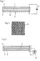
- FIG. 1 schematically shows an embodiment a device according to the invention with a dielectric with a flat surface.
- 2 shows one Hole electrode, as used in FIG. 1 can come.
- 3 shows a further embodiment, where the dielectric on both Pages one active for nucleation or crystal formation Has surface.
- Fig. 4 shows an embodiment with a cylindrical surface.
- 5 shows a section along the line A-A of Fig. 4.
- Die 6 also shows a cylindrical design, where, however, the active surface of the dielectric, which is exposed to the electric field that Interior of a tube thus formed is facing.
- Fig. 7 shows an embodiment in a trap shape.
- the device shown in Fig. 1 has Dielectric 1, for example a polyamide.
- Dielectric 1 for example a polyamide.
- two electrodes 2, 3 are cast in, that of a voltage source 4 with a DC voltage be supplied.
- the electrode 3 is a perforated electrode formed as shown in Fig. 2. So it comes through the holes of the hole electrode 3 Field penetrations that on the active surface 1a of the Dielectric lead to polarizations.
- the active one Surface 1a of the dielectric is exposed to solution 4, from which the germs or crystals on the Surface should grow.
- 1, 2 illustrated embodiment of the invention For example, an increased device Lime deposition on a polyamide surface from a achieve oversaturated aqueous solution 4 with respect to lime.
- Polyamides usually form unbranched chains with recurring carboxamide groups:
- the molecular mass is between 15,000 and 50,000.
- Polyamides are primarily thermoplastic Plastics.
- Polyamide 6 is used as the dielectric.
- the holes in the electrode 3 are circular and have one Diameter of 5 mm.
- the respective polyamide layer has a thickness of 1 mm.
- the amount of the maximum vertical component of the electric field on the surface of the dielectric can be varied from 0 V / m to approx. 2 x 10 5 V / m (linear).
- the device is the actual one according to the invention device operated by an electric field.
- the devices are in the supersaturated solution immersed, one of the devices is a corresponding Potential difference created. After a certain time, the devices will be out of solution taken, dried in a desiccator and the dry weight determined with the analytical balance. The weight difference Dry weight afterwards minus dry weight previously referred to the deposited lime.
- dielectrics are polymers, Crystals, ceramics, metal oxides or glasses.
- Polymers are particularly advantageous because they are Selection of suitable monomers in a simple manner Incorporation of functional groups as actual Allow centers of nucleation.
- the electrodes can with a hardening dielectric be poured into this, as shown in Fig. 1st is shown. But it is also possible to use the electrodes evaporate at least partially as conductive layers or conductivity varnishes or amalgam layers use. Basically, electrolytes are also considered Electrodes conceivable and possible.
- the dielectric and / or the electrical field Generating electrodes can be done using planar epitaxy (Repro technique, mask technique, electron beam lithography) getting produced. So it is possible to form the smallest structures on the surface and hence the crystal or seed growth accordingly influence.
- a fine tuning is apart from a variation of the electrical according to the invention Field also by means of stretching or compressing of the dielectric possible. This can be done by applying a corresponding force or by increasing the temperature or reduction can be achieved.
- FIGS. 1 and 2 shows a variant in which on both sides a middle electrode hole electrodes 3 are arranged through the field penetrations of the electrical Field. 3 shown device two active flat surfaces. The size of the set applied potential and thus the field strength. It would also be possible to use the top and bottom Hole electrode 3 to put on different voltages.
- Fig. 4 acts it is a device with a cylindrical Outer surface.
- the hole electrode is cylindrical curved and around a central central electrode 2 arranged around. 5 shows a corresponding one Cross-section.
- Fig. 6 shows an embodiment in which the Overall, the device is tubular.
- a cylindrical outer electrode 2 surrounds in the dielectric a cylindrical inner electrode 3, which is also in the Dielectric is embedded.
- This inner electrode 3 is designed as a perforated electrode, so that the electrical Field the cylindrical inner surface of the dielectric reached.
- Fig. 7 shows an embodiment in a Fish trap shape.
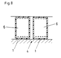
- Electrodes In addition to causing an electrical field through Applying a potential to preferably metallic ones Electrodes also have the option of electrical Generate field in other ways, for example the pyroelectric or the are also suitable piezoelectric effect for field generation. Another preferred embodiment is shown in FIG. 8. There are so-called electrets 6 (these are dielectrics with high permanent electrical dipole moments) used to create the field. Many electrets can be attributed to the ferroelectrics. For example can ceramic materials Barium titanate by cooling temperatures above polarize their Curie point in an electric field. Certain resins, waxes, polyurethanes, Polyethylene and fluorocarbons in a strong electric field are melted, keep the thereby forced alignment of their dipoles when after solidification the field is switched off.
- the electret 6 is in each case through a polymer layer 1 protected against discharge by the liquid.
- This polymer layer also forms the solution exposed dielectric and is also expedient Carrier of active functional groups that act as centers the nucleation or crystallization function.
- An electric field, the one, is particularly favorable field component perpendicular to the surface of the dielectric having.
- the invention further relates to a method for Controlling nucleation or epitaxial growth of crystals from a solution on one Surface of a dielectric.
- the method provides that the dielectric in Area of its surface an adjustable electrical Field is exposed. By this measure can polarize non-polar molecules in the electric field are or already polar molecules in electrical Field.
- crystal nuclei seed crystals
- precipitation and flocculation reactions can be controlled, in particular for physical water treatment (via concentration, shape, structure and size of the nuclei)
Landscapes
- Chemical & Material Sciences (AREA)
- Crystallography & Structural Chemistry (AREA)
- Oral & Maxillofacial Surgery (AREA)
- Metallurgy (AREA)
- Organic Chemistry (AREA)
- Physics & Mathematics (AREA)
- Health & Medical Sciences (AREA)
- Engineering & Computer Science (AREA)
- Thermal Sciences (AREA)
- Materials Engineering (AREA)
- Crystals, And After-Treatments Of Crystals (AREA)
- Physical Or Chemical Processes And Apparatus (AREA)
- Saccharide Compounds (AREA)
- Heterocyclic Carbon Compounds Containing A Hetero Ring Having Oxygen Or Sulfur (AREA)
- Medicines That Contain Protein Lipid Enzymes And Other Medicines (AREA)
- Water Treatment By Electricity Or Magnetism (AREA)
- Inorganic Insulating Materials (AREA)
- Transition And Organic Metals Composition Catalysts For Addition Polymerization (AREA)
- Pretreatment Of Seeds And Plants (AREA)
Applications Claiming Priority (3)
| Application Number | Priority Date | Filing Date | Title |
|---|---|---|---|
| AT69894 | 1994-04-05 | ||
| AT698/94 | 1994-04-05 | ||
| PCT/AT1995/000067 WO1995026931A1 (de) | 1994-04-05 | 1995-04-04 | Verfahren und vorrichtung zur gezielten bildung von keimen oder kristallen |
Publications (2)
| Publication Number | Publication Date |
|---|---|
| EP0754167A1 EP0754167A1 (de) | 1997-01-22 |
| EP0754167B1 true EP0754167B1 (de) | 1998-07-29 |
Family
ID=3497459
Family Applications (1)
| Application Number | Title | Priority Date | Filing Date |
|---|---|---|---|
| EP95915052A Expired - Lifetime EP0754167B1 (de) | 1994-04-05 | 1995-04-04 | Verfahren und vorrichtung zur gezielten bildung von keimen oder kristallen |
Country Status (11)
| Country | Link |
|---|---|
| US (1) | US6001176A (da) |
| EP (1) | EP0754167B1 (da) |
| JP (1) | JPH09510914A (da) |
| CN (1) | CN1147237A (da) |
| AT (1) | ATE168971T1 (da) |
| AU (1) | AU697057B2 (da) |
| CA (1) | CA2187098A1 (da) |
| DE (1) | DE59502994D1 (da) |
| DK (1) | DK0754167T3 (da) |
| ES (1) | ES2122577T3 (da) |
| WO (1) | WO1995026931A1 (da) |
Families Citing this family (8)
| Publication number | Priority date | Publication date | Assignee | Title |
|---|---|---|---|---|
| AT402919B (de) * | 1996-02-01 | 1997-09-25 | Maitron Gmbh | Einrichtung zur physikalischen wasseraufbereitung |
| AT1590U1 (de) * | 1996-10-17 | 1997-08-25 | Maitron Gmbh | Elektrodenanordnung |
| FR2766812B1 (fr) * | 1997-07-31 | 1999-09-24 | Joseph Taillet | Dispositif pour le traitement electrique d'un electrolyte liquide, en particulier d'une eau a epurer |
| JP2005521553A (ja) * | 2002-04-02 | 2005-07-21 | イー・アイ・デュポン・ドウ・ヌムール・アンド・カンパニー | 結晶成長に使用される装置および方法 |
| WO2010100847A1 (ja) * | 2009-03-03 | 2010-09-10 | 独立行政法人国立高等専門学校機構 | 生体高分子の結晶化装置、生体高分子の結晶化溶液セル、生体高分子の配向制御方法、生体高分子の結晶化方法、及び生体高分子の結晶 |
| WO2012027398A2 (en) | 2010-08-23 | 2012-03-01 | Massachusetts Institute Of Technology | Compositions, methods, and systems relating to controlled crystallization and/or nucleation of molecular species |
| US9822467B2 (en) | 2011-11-15 | 2017-11-21 | Massachusetts Institute Of Technology | Methods and systems relating to the selection of substrates comprising crystalline templates for the controlled crystallization of molecular species |
| CN110354528B (zh) * | 2019-08-21 | 2021-11-19 | 贺剑 | 溶液结晶系统及促进溶液结晶的方法 |
Family Cites Families (9)
| Publication number | Priority date | Publication date | Assignee | Title |
|---|---|---|---|---|
| GB646882A (en) * | 1947-06-16 | 1950-11-29 | Hermann Loosli | A new or improved method of and means for preventing and removing incrustations uponcontainers for liquids |
| US5214300A (en) * | 1970-09-28 | 1993-05-25 | Ramtron Corporation | Monolithic semiconductor integrated circuit ferroelectric memory device |
| US4529488A (en) * | 1982-06-29 | 1985-07-16 | Nippon Gohsei Kagaku Kogyo Kabushiki Kaisha | Process for depositing salts |
| ATA15685A (de) * | 1985-01-22 | 1988-07-15 | Maitron Gmbh | Vorrichtung zur beseitigung von kesselstein und korrosion bzw. zum verhueten der bildung von kesselstein und korrosion |
| JPS63501349A (ja) * | 1986-01-21 | 1988-05-26 | マイトロン ゲラ−テバウ ゲス.エム.ベ−.ハ− ウント カンパニ− カ−・ゲ− | 水溶液の処理方法とその処理を行なうための装置 |
| CA1265094A (en) * | 1986-08-27 | 1990-01-30 | 671135 Ontario Limited | Electrostatic field generator for liquid treatment |
| FR2640955B1 (da) * | 1988-12-26 | 1991-11-29 | Taillet Joseph | |
| US5759923A (en) * | 1991-02-25 | 1998-06-02 | Symetrix Corporation | Method and apparatus for fabricating silicon dioxide and silicon glass layers in integrated circuits |
| US5681457A (en) * | 1995-10-10 | 1997-10-28 | Mahoney; Robert F. | Electrodynamic fluid treatment system |
-
1995
- 1995-04-04 US US08/718,328 patent/US6001176A/en not_active Expired - Lifetime
- 1995-04-04 ES ES95915052T patent/ES2122577T3/es not_active Expired - Lifetime
- 1995-04-04 DE DE59502994T patent/DE59502994D1/de not_active Expired - Lifetime
- 1995-04-04 JP JP7525299A patent/JPH09510914A/ja active Pending
- 1995-04-04 DK DK95915052T patent/DK0754167T3/da active
- 1995-04-04 WO PCT/AT1995/000067 patent/WO1995026931A1/de not_active Ceased
- 1995-04-04 EP EP95915052A patent/EP0754167B1/de not_active Expired - Lifetime
- 1995-04-04 AU AU22080/95A patent/AU697057B2/en not_active Ceased
- 1995-04-04 AT AT95915052T patent/ATE168971T1/de not_active IP Right Cessation
- 1995-04-04 CN CN95192880A patent/CN1147237A/zh active Pending
- 1995-04-04 CA CA002187098A patent/CA2187098A1/en not_active Abandoned
Also Published As
| Publication number | Publication date |
|---|---|
| DE59502994D1 (de) | 1998-09-03 |
| AU697057B2 (en) | 1998-09-24 |
| ATE168971T1 (de) | 1998-08-15 |
| ES2122577T3 (es) | 1998-12-16 |
| AU2208095A (en) | 1995-10-23 |
| JPH09510914A (ja) | 1997-11-04 |
| CA2187098A1 (en) | 1995-10-12 |
| CN1147237A (zh) | 1997-04-09 |
| US6001176A (en) | 1999-12-14 |
| DK0754167T3 (da) | 1999-05-03 |
| EP0754167A1 (de) | 1997-01-22 |
| WO1995026931A1 (de) | 1995-10-12 |
Similar Documents
| Publication | Publication Date | Title |
|---|---|---|
| DE68922599T2 (de) | Elektrisches Behandlungsgerät für Elektrolyten mit hoher Leitfähigkeit, insbesondere Leitungs- oder Flusswasser. | |
| DE4400955C2 (de) | Adhäsionssteuerbare Oberflächenstruktur | |
| DE60216039T2 (de) | Piezoelektrischer Einkristall mit kontrollierter Domänenstruktur | |
| DE69204187T2 (de) | Elektrisch regenerierbare Entmineralisierungsvorrichtung. | |
| EP1062032B1 (de) | Verfahren und vorrichtung zum verkapseln von mikrobiellen, pflanzlichen und tierischen zellen bzw. von biologischen und chemischen substanzen | |
| DE2538717C3 (de) | Verfahren zur Herstellung eines aus einer polarisierten Kunststoffolie bestehenden elektrischen Bauelementes | |
| EP0754167B1 (de) | Verfahren und vorrichtung zur gezielten bildung von keimen oder kristallen | |
| DE2455205A1 (de) | Verfahren und einrichtung zur elektrischen reinigung und entkeimung von fluessigkeiten | |
| DE3875122T2 (de) | System fuer elektrolytische behandlung einer fluessigkeit. | |
| AT410805B (de) | Verfahren zum erzeugen einer schicht funktioneller moleküle | |
| EP1002765B1 (de) | Vorrichtung und Verfahren zur Behandlung von Wasser gegen Kalkablagerungen | |
| EP1902311A2 (de) | Gate-kontrollierter atomarer schalter | |
| EP0128565B1 (de) | Verfahren und Vorrichtung zur Fusion von Zellen | |
| DE10009643A1 (de) | Vorrichtung und Verfahren zum Behandeln von Verunreinigungen enthaltendem Wasser | |
| DE69417786T2 (de) | Magnetisch arbeitende Vorrichtung zur Behandlung von Kalziumbikarbonate enthaltendem Leitungswasser | |
| DE69807571T2 (de) | Verfahren und Vorrichtung zum Ätzen | |
| EP3781524B1 (de) | Elektrochemischer fällungsreaktor | |
| EP1125895B1 (de) | Verfahren sowie Vorrichtung zur Verhütung von Wasserstein in wasserführenden Systemen | |
| DE19929542B4 (de) | Flächige Anordnung von Stimulationselektroden auf einem Chip und Herstellungsverfahren dazu und Verwendung als Retina-Implantat | |
| DE3343586A1 (de) | Verfahren zur entkeimung eines mediums und vorrichtung zur durchfuehrung | |
| DE2307608A1 (de) | Verfahren und geraet zur nega-katalytischen aktivierung von freiem oder organischem wasser | |
| DE3218081A1 (de) | Elektretvorrichtung | |
| DE60220289T2 (de) | Verfahren und vorrichtung zur behandlung von flüssigkeiten | |
| DE3871605T2 (de) | Verfahren zur behandlung von polymerischen gegenstaenden durch coronaentladung. | |
| AT224179B (de) | Biegungsschwinger aus plättchenförmigem, elektrostriktivem Material |
Legal Events
| Date | Code | Title | Description |
|---|---|---|---|
| PUAI | Public reference made under article 153(3) epc to a published international application that has entered the european phase |
Free format text: ORIGINAL CODE: 0009012 |
|
| 17P | Request for examination filed |
Effective date: 19961026 |
|
| AK | Designated contracting states |
Kind code of ref document: A1 Designated state(s): AT BE CH DE DK ES FR GB GR IE IT LI NL PT SE |
|
| 17Q | First examination report despatched |
Effective date: 19970311 |
|
| GRAG | Despatch of communication of intention to grant |
Free format text: ORIGINAL CODE: EPIDOS AGRA |
|
| GRAG | Despatch of communication of intention to grant |
Free format text: ORIGINAL CODE: EPIDOS AGRA |
|
| GRAH | Despatch of communication of intention to grant a patent |
Free format text: ORIGINAL CODE: EPIDOS IGRA |
|
| GRAH | Despatch of communication of intention to grant a patent |
Free format text: ORIGINAL CODE: EPIDOS IGRA |
|
| GRAA | (expected) grant |
Free format text: ORIGINAL CODE: 0009210 |
|
| AK | Designated contracting states |
Kind code of ref document: B1 Designated state(s): AT BE CH DE DK ES FR GB GR IE IT LI NL PT SE |
|
| PG25 | Lapsed in a contracting state [announced via postgrant information from national office to epo] |
Ref country code: GR Free format text: LAPSE BECAUSE OF NON-PAYMENT OF DUE FEES Effective date: 19980729 |
|
| REF | Corresponds to: |
Ref document number: 168971 Country of ref document: AT Date of ref document: 19980815 Kind code of ref document: T |
|
| REG | Reference to a national code |
Ref country code: CH Ref legal event code: EP |
|
| REF | Corresponds to: |
Ref document number: 59502994 Country of ref document: DE Date of ref document: 19980903 |
|
| PG25 | Lapsed in a contracting state [announced via postgrant information from national office to epo] |
Ref country code: SE Free format text: LAPSE BECAUSE OF FAILURE TO SUBMIT A TRANSLATION OF THE DESCRIPTION OR TO PAY THE FEE WITHIN THE PRESCRIBED TIME-LIMIT Effective date: 19981029 Ref country code: PT Free format text: LAPSE BECAUSE OF FAILURE TO SUBMIT A TRANSLATION OF THE DESCRIPTION OR TO PAY THE FEE WITHIN THE PRESCRIBED TIME-LIMIT Effective date: 19981029 |
|
| REG | Reference to a national code |
Ref country code: IE Ref legal event code: FG4D Free format text: GERMAN |
|
| GBT | Gb: translation of ep patent filed (gb section 77(6)(a)/1977) |
Effective date: 19981104 |
|
| REG | Reference to a national code |
Ref country code: CH Ref legal event code: NV Representative=s name: ISLER & PEDRAZZINI AG |
|
| REG | Reference to a national code |
Ref country code: ES Ref legal event code: FG2A Ref document number: 2122577 Country of ref document: ES Kind code of ref document: T3 |
|
| ET | Fr: translation filed | ||
| PG25 | Lapsed in a contracting state [announced via postgrant information from national office to epo] |
Ref country code: BE Free format text: LAPSE BECAUSE OF NON-PAYMENT OF DUE FEES Effective date: 19990430 |
|
| REG | Reference to a national code |
Ref country code: DK Ref legal event code: T3 |
|
| PG25 | Lapsed in a contracting state [announced via postgrant information from national office to epo] |
Ref country code: IE Free format text: LAPSE BECAUSE OF NON-PAYMENT OF DUE FEES Effective date: 19990504 |
|
| REG | Reference to a national code |
Ref country code: CH Ref legal event code: PUEA Free format text: MAITRON CHEMIEFREIE WASSERBEHANDLUNG G.M.B.H. TRANSFER- DR. KLAUS LEITER;DR. GERHARD WALDER |
|
| PLBE | No opposition filed within time limit |
Free format text: ORIGINAL CODE: 0009261 |
|
| STAA | Information on the status of an ep patent application or granted ep patent |
Free format text: STATUS: NO OPPOSITION FILED WITHIN TIME LIMIT |
|
| REG | Reference to a national code |
Ref country code: FR Ref legal event code: TQ |
|
| REG | Reference to a national code |
Ref country code: IE Ref legal event code: FD4D Ref country code: GB Ref legal event code: 732E |
|
| 26N | No opposition filed | ||
| NLS | Nl: assignments of ep-patents |
Owner name: WALDER, DR. GERHARDT -;LEITER, DR. KLAUS - |
|
| BERE | Be: lapsed |
Owner name: MAITRON CHEMIEFREIE WASSERBEHANDLUNG G.M.B.H. Effective date: 19990430 |
|
| PGFP | Annual fee paid to national office [announced via postgrant information from national office to epo] |
Ref country code: ES Payment date: 20010419 Year of fee payment: 7 |
|
| PGFP | Annual fee paid to national office [announced via postgrant information from national office to epo] |
Ref country code: DK Payment date: 20010423 Year of fee payment: 7 |
|
| PGFP | Annual fee paid to national office [announced via postgrant information from national office to epo] |
Ref country code: FR Payment date: 20010426 Year of fee payment: 7 Ref country code: CH Payment date: 20010426 Year of fee payment: 7 |
|
| PGFP | Annual fee paid to national office [announced via postgrant information from national office to epo] |
Ref country code: NL Payment date: 20010430 Year of fee payment: 7 |
|
| REG | Reference to a national code |
Ref country code: GB Ref legal event code: IF02 |
|
| PG25 | Lapsed in a contracting state [announced via postgrant information from national office to epo] |
Ref country code: ES Free format text: LAPSE BECAUSE OF NON-PAYMENT OF DUE FEES Effective date: 20020405 |
|
| PG25 | Lapsed in a contracting state [announced via postgrant information from national office to epo] |
Ref country code: LI Free format text: LAPSE BECAUSE OF NON-PAYMENT OF DUE FEES Effective date: 20020430 Ref country code: DK Free format text: LAPSE BECAUSE OF NON-PAYMENT OF DUE FEES Effective date: 20020430 Ref country code: CH Free format text: LAPSE BECAUSE OF NON-PAYMENT OF DUE FEES Effective date: 20020430 |
|
| PG25 | Lapsed in a contracting state [announced via postgrant information from national office to epo] |
Ref country code: NL Free format text: LAPSE BECAUSE OF NON-PAYMENT OF DUE FEES Effective date: 20021101 |
|
| REG | Reference to a national code |
Ref country code: CH Ref legal event code: PL |
|
| REG | Reference to a national code |
Ref country code: DK Ref legal event code: EBP |
|
| PG25 | Lapsed in a contracting state [announced via postgrant information from national office to epo] |
Ref country code: FR Free format text: LAPSE BECAUSE OF NON-PAYMENT OF DUE FEES Effective date: 20021231 |
|
| NLV4 | Nl: lapsed or anulled due to non-payment of the annual fee |
Effective date: 20021101 |
|
| REG | Reference to a national code |
Ref country code: FR Ref legal event code: ST |
|
| PGFP | Annual fee paid to national office [announced via postgrant information from national office to epo] |
Ref country code: GB Payment date: 20030403 Year of fee payment: 9 |
|
| PG25 | Lapsed in a contracting state [announced via postgrant information from national office to epo] |
Ref country code: GB Free format text: LAPSE BECAUSE OF NON-PAYMENT OF DUE FEES Effective date: 20040404 |
|
| PGFP | Annual fee paid to national office [announced via postgrant information from national office to epo] |
Ref country code: AT Payment date: 20040414 Year of fee payment: 10 |
|
| REG | Reference to a national code |
Ref country code: ES Ref legal event code: FD2A Effective date: 20030514 |
|
| GBPC | Gb: european patent ceased through non-payment of renewal fee | ||
| PG25 | Lapsed in a contracting state [announced via postgrant information from national office to epo] |
Ref country code: IT Free format text: LAPSE BECAUSE OF NON-PAYMENT OF DUE FEES Effective date: 20050404 Ref country code: AT Free format text: LAPSE BECAUSE OF NON-PAYMENT OF DUE FEES Effective date: 20050404 |
|
| REG | Reference to a national code |
Ref country code: DE Ref legal event code: R081 Ref document number: 59502994 Country of ref document: DE Owner name: WCR TECHNOLOGIE GMBH, DE Free format text: FORMER OWNERS: WALDER, GERHARD, DR., ZIRL, AT; LEITER, KLAUS, DR., VOELS, AT Effective date: 20110302 Ref country code: DE Ref legal event code: R081 Ref document number: 59502994 Country of ref document: DE Owner name: WCR TECHNOLOGIE GMBH, DE Free format text: FORMER OWNER: GERHARD WALDER,KLAUS LEITER, , AT Effective date: 20110302 |
|
| PGFP | Annual fee paid to national office [announced via postgrant information from national office to epo] |
Ref country code: DE Payment date: 20120427 Year of fee payment: 18 |
|
| PG25 | Lapsed in a contracting state [announced via postgrant information from national office to epo] |
Ref country code: DE Free format text: LAPSE BECAUSE OF NON-PAYMENT OF DUE FEES Effective date: 20131101 |
|
| REG | Reference to a national code |
Ref country code: DE Ref legal event code: R119 Ref document number: 59502994 Country of ref document: DE Effective date: 20131101 |