EP0753864A1 - Chip type composite electronic component - Google Patents
Chip type composite electronic component Download PDFInfo
- Publication number
- EP0753864A1 EP0753864A1 EP96900175A EP96900175A EP0753864A1 EP 0753864 A1 EP0753864 A1 EP 0753864A1 EP 96900175 A EP96900175 A EP 96900175A EP 96900175 A EP96900175 A EP 96900175A EP 0753864 A1 EP0753864 A1 EP 0753864A1
- Authority
- EP
- European Patent Office
- Prior art keywords
- common electrode
- layer
- individual electrodes
- solder
- thickness
- Prior art date
- Legal status (The legal status is an assumption and is not a legal conclusion. Google has not performed a legal analysis and makes no representation as to the accuracy of the status listed.)
- Granted
Links
Images


Classifications
-
- H—ELECTRICITY
- H01—ELECTRIC ELEMENTS
- H01C—RESISTORS
- H01C13/00—Resistors not provided for elsewhere
- H01C13/02—Structural combinations of resistors
Definitions
- the present invention relates to a chip-type composite electronic component which comprises a common electrode, a plurality of individual electrode, and a plurality of electronic elements each interposed between each of the individual electrodes and the common electrode.
- chip-type composite electronic components include a composite resistor incorporating a plurality of resistor elements, a composite capacitor incorporating a plurality of capacitor elements, and a composite diode incorporating a plurality of diode elements.
- a typical composite resistor comprises a single substrate, a common electrode formed on the substrate, a plurality of individual electrodes formed on the substrate to be spaced from the common electrode, and a plurality of resistor elements (film-like resistor elements) each interposed between each of the individual electrodes and the common electrode.
- Each of the common electrode and individual electrodes includes a thick film layer of silver-palladium alloy, a nickel layer plated on the thick film layer, and a solder layer plated on the nickel layer.
- the thickness of the nickel and solder layers of the common electrode increases at an extremely higher rate than the thickness of the nickel and solder layers of each individual electrode as the resistance of the film-like resistor elements increases. This can be understood by referring to the "no agitator" column in the table shown in Fig. 7.
- the "no agitator" column in the Fig. 7 table shows, with respect to a multiplicity of prior art chip-type composite resistors for each of different resistance values of resistor elements, a ratio between the thickness (average) of the solder layers of the common electrodes and the thickness (average) of the solder layers of the individual electrodes.
- the table also shows a ratio between the thickness (average) of the nickel layers of the common electrodes and the thickness (average) of the nickel layers of the individual electrodes.
- the thickness of the solder layer of the common electrode is 2.20 times as great as the thickness of the solder layer of the individual electrodes, whereas the thickness of the nickel layer of the common electrode is 2.78 times as great as the thickness of the nickel layer of the individual electrodes.
- the resistance of the resistor elements is 47 K ⁇
- the thickness of the solder layer of the common electrode is 3.04 times as great as the thickness of the solder layer of the individual electrodes, whereas the thickness of the nickel layer of the common electrode is 3.44 times as great as the thickness of the nickel layer of the individual electrodes.
- the thickness of the solder layer of the common electrode is 5.02 times as great as the thickness of the solder layer of the individual electrodes, whereas the thickness of the nickel layer of the common electrode is 4.29 times as great as the thickness of the nickel layer of the individual electrodes.
- the individual electrodes connected to the resistor elements having a large electrical resistance will suffer difficulty in forming nickel and solder layers
- the nickel and solder layers of the common electrode having an extremely low resistance will tend to have an excessively large thickness if the respective thickness of nickel and solder layers of the individual electrode is made to have a predetermined value.
- the solder layer of the common electrode becomes extremely large.
- hydrogen gas remains inside the solder as foams which cause the solder surfaces to be greatly roughened.
- the solder layer of the common electrode melts to generate hydrogen gas which is occluded in the solder layer. If the solder layer has a small thickness, the generated hydrogen gas will escape to the exterior without remaining inside the solder while the solder is still in a molten state.
- the thickness of the solder layer is large, a portion of the hydrogen gas generated at a deep position of the solder layer cannot go out before solidification of the solder, consequently remaining as foams within the solder.
- solder surfaces at the common electrode are greatly roughened due to the remaining hydrogen gas foams.
- Such surface roughening can be a cause for an erroneous detection when automatically detecting the presence, position or posture of the chip-type composite electronic component by light reflection at the solder surface for example.
- the thickness of the nickel layer 14a becomes extremely large if the direct current resistance is large, the nickel layer is deformed under thermal stresses caused by temperature fluctuations after soldering, thereby lifting up and breaking the thick film layer.
- the present invention is proposed in view of the above-described problems of the prior art and aims to provide a chip-type composite electronic component wherein solder surfaces at a common electrode are not largely roughened after soldering.
- Another object of the present invention is to provide a chip-type composite electronic component wherein thick film layers are prevented from breaking due to thermal deformation of nickel layers.
- a chip-type composite electronic component comprising: an insulating substrate; a common electrode formed on the substrate; a plurality of individual electrodes formed on the substrate to be spaced from the common electrode, and a plurality of electronic elements each interposed between each of the individual electrodes and the common electrode; wherein each of the common electrode and individual electrodes has a plated solder layer as an outermost layer; characterized that each of the electronic elements has a direct current resistance of no less than 47K ⁇ , the solder layer of the common electrode having a layer thickness which is no more than 2.9 times as great as that of the solder layer of the individual electrodes.
- the thickness of the solder layer of the common electrode is limited only to no more than 2.9 times as great as the thickness of the solder layer of each individual electrode.
- the solder layer of the common electrode will not have an excessively large thickness.
- the solder layer of the common layer melts with the solder paste to generate hydrogen gas occluded in the solder layer.
- hydrogen gas escapes to the exterior without remaining inside the solder while the solder is still in molten state. In this way, hydrogen gas does not remain inside the solder as foams, so that the solder surfaces at the common electrode is prevented from being largely roughened.
- a chip-type composite electronic component comprising: an insulating substrate; a common electrode formed on the substrate; a plurality of individual electrodes formed on the substrate to be spaced from the common electrode, and a plurality of electronic elements each interposed between each of the individual electrodes and the common electrode; wherein each of the common electrode and individual electrodes has a plated nickel layer; characterized that each of the electronic elements has a direct current resistance of no less than 47 K ⁇ , the nickel layer of the common electrode having a layer thickness which is no more than 3.2 times as great as that of the nickel layer of the individual electrodes.
- the thickness of the nickel layer of the common electrode is limited only to no more than 3.2 times as great as the thickness of the nickel layer of each individual electrode.
- the nickel layer of the common electrode will not have an excessively large thickness. Therefore, the underlying thick film layer can be prevented from being lifted to break due to thermal stresses imparted to the nickel layer by temperature fluctuations after soldering.
- the electronic elements are resistors which are equal to each other in resistance.
- each of the electronic elements may be a capacitor which has a direct current resistance of no less than 47 K ⁇ when sufficiently charged.
- a capacitor exhibits a direct current resistance of nearly zero in the absence of any charge, its direct current resistance increases substantially to infinity when completely charged. Therefore, a capacitor is deemed to provide a large direct current resistance at the time of plating solder layers, thus falling within the scope of the present invention.
- each of the electronic elements may be a diode which has a reverse direct current resistance of no less than 47 K ⁇ .
- a diode which has a reverse direct current resistance of no less than 47 K ⁇ .
- a diode though it exhibits a forward direct current resistance of nearly zero, its reverse direct current resistance is substantially infinite. Therefore, a diode is deemed to provide a large direct current resistance at the time of plating solder layers, thus falling in the scope of the present invention.
- An example of diode is a leadless diode.
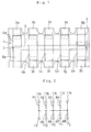
- a substrate 1 has an obverse surface formed with a common electrode 2, a plurality of individual electrodes 3a-3h, and a plurality of film-like resistor elements 4a-4e.
- the substrate 1 may be made of an insulating material such as ceramic and has a generally rectangular shape. However, the shape of the substrate 1 is not limitative.
- the common electrode 2 includes a main strip portion 5 and common terminals 6a, 6b at both ends of the main strip portion 5.
- the main strip portion 5 of the common electrode 2 is located at the widthwise center of the substrate 1 and extends longitudinally of the substrate 1 to both ends thereof.
- One common terminal 6a (hereafter referred to as “first common terminal”) of the common electrode 2 overlaps the main strip portion 5 and extends beyond one longitudinal edge (hereafter referred to as "first longitudinal edge") of the substrate 1 onto the reverse surface thereof (see Fig. 4A).
- the other common terminal 6b (hereafter referred to as “second common terminal”) of the common electrode 2 is formed integrally with the main strip portion 5 and extends beyond the other longitudinal edge (hereafter referred to as "second longitudinal edge") of the substrate 1 onto the reverse surface thereof (though not shown but similar to the first common terminal 6a shown in Fig. 4A).
- the plurality of individual electrodes 3a-3h are divided into a first group of individual electrodes 3a-3d arranged adjacent to the first longitudinal edge of the substrate 1, and a second group of individual electrodes 3e-3h arranged adjacent to the second longitudinal edge of the substrate 1.
- the individual electrodes 3a-3d of the first group which are constantly spaced from each other longitudinally of the substrate 1 and disposed in parallel to the first common terminal 6a, extend beyond the first longitudinal edge of the substrate 1 onto the reverse surface thereof (though not shown but similar to the first common terminal 6a shown in Fig. 4A).
- the individual electrodes 3e-3h of the second group which are constantly spaced from each other longitudinally of the substrate 1 and disposed in parallel to the second common terminal 6b, extend beyond the second longitudinal edge of the substrate 1 onto the reverse surface thereof (though not shown but similar to the first common terminal 6a shown in Fig. 4A).
- the individual electrode 3a of the first group is aligned with the second common terminal 6b of the common electrode 2 transversely of the substrate 1.
- the individual electrode 3h of the second group is aligned with the first common terminal 6a of the common electrode 2.
- the individual electrodes 3b-3d of the first group are aligned respectively with the individual electrodes 3e-3g of the second group.
- the film-like resistor element 4a is formed to overlap the main strip portion 5 of the common electrode 2 and the individual electrode 3a of the first group.
- the film-like resistor element 4e is formed to overlap the main strip portion 5 of the common electrode 2 and the individual electrode 3h of the second group.
- the resistor elements 4b, 4c, 4d are formed to respectively overlap the individual electrodes 3b, 3c, 3d of the first group as well as the individual electrodes 3e, 3f, 3g of the second group while centrally overlapping the main strip portion 5 of the common electrode 2.
- Fig. 2 shows an equivalent circuit of the above-described chip-type composite electronic component.
- the equivalent circuit comprises a plurality of resistors R1-R8 and a plurality of terminals 11a-11j.
- the resistors R1-R4 are connected respectively to the terminals 11a-11d at one end, whereas the resistors R5-R8 are connected respectively to the terminals 11g-11j at one end.
- the resistors R1-R8 are connected respectively to the terminals 11e, 11f at the other end.
- the terminals 11a-11d are provided respectively by the individual electrodes 3a-3d of the first group, whereas the terminals 11e-11h are provided respectively by the individual electrodes 3e-3h of the second group.
- the terminal 11e is constituted by the first common terminal 6a of the common electrode 2, whereas the terminal 11f is constituted by the second common terminal 6b.
- the resistors R1, R8 are provided respectively by the resistor elements 4a, 4e, whereas the resistors R2-R7 are provided respectively by the resistor elements 4b-4d which are divided by the main strip portion 5 of the common electrode 2.
- each of the resistors R1-R8 has a resistance of 100K ⁇ .
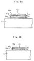
- the first common terminal 6a of the common electrode 2 comprises a thick film layer 13a made of silver-palladium alloy, a nickel layer 14a plated on the thick film layer 13a, and a solder layer 15a (tin-lead alloy) plated on the nickel layer 14a.
- a thick film layer 13a made of silver-palladium alloy
- a nickel layer 14a plated on the thick film layer 13a
- a solder layer 15a titanium-lead alloy
- the main strip portion of the common electrode 2 comprises only a thick film layer made of silver-palladium alloy (like the thick film layer 13a shown in Fig. 3A).
- the individual electrode 3a also comprises a thick film layer 13b made of silver-palladium alloy, a nickel layer 14b plated on the thick film layer 13a, and a solder layer 15b (tin-lead alloy) plated on the nickel layer 14a.
- a thick film layer 13b made of silver-palladium alloy
- a nickel layer 14b plated on the thick film layer 13a
- a solder layer 15b solder layer 15b (tin-lead alloy) plated on the nickel layer 14a.
- solder layer 15b titanium-lead alloy
- the thickness t1 of the solder layer 15a of the respective common terminals 6a, 6b is 2.68 times as great as the thickness t2 of the solder layer 15b of the respective individual electrodes 3a-3h. Further, the thickness t3 of the nickel layer 14a of the respective common terminals 6a, 6b is 2.93 times as great as the thickness t4 of the nickel layer 14b of the respective individual electrodes 3a-3h.
- the individual electrodes 3a-3h and the respective common terminals 6a, 6b together with the main strip portion 5 of the common electrode 2 are covered by a coating layer 7 made of an insulating material.
- the portions of the individual electrodes 3a-3h and respective common terminals 6a, 6b covered by the coating layer 7 consist only of the thick film layer 13a or 13b and are not plated with nickel nor solder.
- Figs. 3A and 3B are sections taken at a position of the first common electrode 6a and individual electrode 3a not covered by the coating layer 7.
- the thickness t1 of the solder layer 15a of the respective common terminals 6a, 6b which is 2.68 times as great as the thickness t2 of the solder layer 15b of the respective individual electrodes 3a-3h, is relatively small, corresponding roughly to a half of the solder layer thickness encountered in a prior art chip-type composite.
- the solder surfaces at the respective common terminal 6a, 6b are prevented from being greatly roughened due to foam formation.
- the solder layer 15a of the first common terminal 6a melts to merge with the solder paste 18.
- hydrogen occluded in the solder layer 15a is generated as hydrogen gas.
- the thus generated hydrogen gas tends to escape to the exterior while the solder paste 18 is still in its molten state.
- the thickness of the solder layer 15a is large, a portion of the hydrogen gas generated at a deep position of the solder layer 15a cannot go out before solidification of the solder paste 18, consequently remaining as foams within the solder paste 18. Due to such foams, the surfaces of the solder paste 18, i.e., the solder surfaces at the common terminal 6a, are greatly roughened, as experienced in a prior art chip-type composite electronic component.
- the thickness of the solder layer 15a is smaller than conventionally possible, the generated hydrogen gas can sufficiently escape out before solidification of the solder paste 18.
- the surfaces of the solder paste 18, i.e., the solder surfaces at the common terminal 6a, are prevented from being greatly roughened due to foam formation.
- the thickness t3 of the nickel layer 14a which is 2.93 times as great as the thickness t4 of the nickel layer 14b, is also relatively small (corresponding roughly to 3/4 of the nickel layer thickness encountered in a prior art chip-type composite electronic component, so that the thick film layer 13a can be prevented from being lifted to break due to thermal stresses imparted to the nickel layer 14a by temperature fluctuations after soldering.
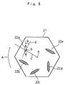
- the nickel layers 14a, 14b and solder layers 15a, 15b of the chip-type composite electronic component according to the illustrated embodiment may be conveniently formed by using such a plating barrel apparatus as is schematically illustrated in Figs. 5 and 6.
- the plating barrel apparatus includes a plating barrel body 21 in which five agitating plates 22a-22e are arranged. Each of the agitating plates 22a-22e is inclined relative to a straight line which is perpendicular to another straight line passing through the rotational center of the plating barrel body 21 and the center of the respective agitating plates 22a-22e.
- the agitating plate 22a for example is inclined by an angle ⁇ relative to a straight line (d) which is perpendicular to another straight line (c) passing through the rotational center (a) of the plating barrel body 21 and the center (b) of the agitating plate 22a.
- This inclination angle ⁇ also applies to the other agitating plates 22b-22e.
- the barrel body 21 is formed with a multiplicity of pores (not shown) for allowing ingress of a plating liquid into the barrel body 21.
- a multiplicity of chip-type composite electronic components are loaded into the plating barrel body 21 together with steel shots and ceramic balls, and the barrel body 21 is immersed in a plating liquid (plating liquid for nickel plating or solder plating).
- a plating liquid plating liquid for nickel plating or solder plating.
- the multiplicity of chip-type composite electronic components within the plating barrel body 21 will rarely suffer variations, from component to component, in the rate or speed of forming nickel layers 14a, 14b or solder layers 15a, 15b.
- the respective thickness of nickel layers 14a, 14b and solder layers 15a, 15b is adjusted to have a predetermined value with respect to electronic components undergoing slower layer formation, the nickel layers 14a, 14b and solder layers 15a, 15b for other electronic components undergoing faster layer formation can be prevented from growing to have an excessively large thickness.
- the individual electrodes 3a-3h connected to the resister elements 4a-4e having a large electrical resistance will suffer difficulty in forming nickel layers 14b or solder layers 15b.
- the agitating plates 22a-22e inside the barrel body 21 even if the respective thickness of nickel layers 14b and solder layers 15b for each of the individual electrode is adjusted to have a predetermined value, the nickel layers 14a and solder layers 15a for the common electrode 2 having an extremely low resistance can be prevented from growing to have an excessively large thickness.
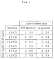
- Figs. 5 and 6 use was made of the plating barrel apparatus shown in Figs. 5 and 6 as well as another plating barrel apparatus having no agitating plate for forming plated nickel layers 14a, 14b and solder layers 15a, 15b with respect to a multiplicity of chip-type composite electronic components. Then, the average thickness of the nickel layers 14a for the common electrode 2 was divided by the average thickness of the nickel layers 14b for the individual electrodes 3a-3h to give a ratio. Similarly, the average thickness of the solder layers 15a for the common electrode 2 was divided by the average thickness of the solder layers 15b for the individual electrodes 3a-3h to give a ratio. Such comparison was performed with respect to different resistance values of resistor elements 4a-4e which included 10 K ⁇ , 47K ⁇ and 100K ⁇ . The results are shown in Fig. 7.
- a ratio of 2.33 is obtained in case the resistors R1-R8 (Fig. 2) have a resistance of 10K ⁇ , 2.37 for 47 K ⁇ , and 2.68 for 100K ⁇ .
- a ratio of 2.35 is obtained in case the resistors R1-R8 have a resistance of 10 K ⁇ , 3.20 for 47 K ⁇ , and 2.93 for 100K ⁇ .
- the thickness of the solder layer 15a at the common electrode 2 tends to be unduly larger than the thickness of the solder layer 15b at each of the individual electrodes 3a-3h connected to the resistors R1-R8 if the resistance of the resistors R1-R8 is no less than 47K ⁇ . This also applies to the nickel layers 14a, 14b.
- the elements interposed between the respective individual electrode 3a-3h and the common electrode 2 are the film-like resistor elements R1-R8 constituting the resistors R1-R8 which are equal in resistance.
- the respective resistors R1-R8 may not be mutually equal in resistance as long as the resistance is no less than 47K ⁇ at the lowest.
- the elements interposed between the respective individual electrode 3a-3h and the common electrode 2 may be capacitors which exhibit a direct current resistance of no less than 47 K ⁇ when sufficiently charged, or diodes having a reverse direct current resistance of no less 47K ⁇ .
- capacitors or diodes though they do not always exhibit a direct current resistance of no less than 47K ⁇ , they may exhibit a high resistance of no less than 47 K ⁇ depending on their charging state or polarity, so that there will be a difference in plated layer thickness between the common electrode 2 and each of the individual electrodes 3a-3h.
- Such a difference can be reduced by using the plating barrel apparatus with the agitating plates 22a-22e for plating the nickel layers 14a, 14b and solder layers 15a, 15b.
Landscapes
- Engineering & Computer Science (AREA)
- Microelectronics & Electronic Packaging (AREA)
- Details Of Resistors (AREA)
- Non-Adjustable Resistors (AREA)
- Thermistors And Varistors (AREA)
- Apparatuses And Processes For Manufacturing Resistors (AREA)
- Fixed Capacitors And Capacitor Manufacturing Machines (AREA)
Abstract
Description
- The present invention relates to a chip-type composite electronic component which comprises a common electrode, a plurality of individual electrode, and a plurality of electronic elements each interposed between each of the individual electrodes and the common electrode.
- Examples of chip-type composite electronic components include a composite resistor incorporating a plurality of resistor elements, a composite capacitor incorporating a plurality of capacitor elements, and a composite diode incorporating a plurality of diode elements.
- Of these, a typical composite resistor comprises a single substrate, a common electrode formed on the substrate, a plurality of individual electrodes formed on the substrate to be spaced from the common electrode, and a plurality of resistor elements (film-like resistor elements) each interposed between each of the individual electrodes and the common electrode. Each of the common electrode and individual electrodes includes a thick film layer of silver-palladium alloy, a nickel layer plated on the thick film layer, and a solder layer plated on the nickel layer.
- With the prior art chip-type composite resistor having the above-described structure, the thickness of the nickel and solder layers of the common electrode increases at an extremely higher rate than the thickness of the nickel and solder layers of each individual electrode as the resistance of the film-like resistor elements increases. This can be understood by referring to the "no agitator" column in the table shown in Fig. 7.
- Specifically, the "no agitator" column in the Fig. 7 table shows, with respect to a multiplicity of prior art chip-type composite resistors for each of different resistance values of resistor elements, a ratio between the thickness (average) of the solder layers of the common electrodes and the thickness (average) of the solder layers of the individual electrodes. The table also shows a ratio between the thickness (average) of the nickel layers of the common electrodes and the thickness (average) of the nickel layers of the individual electrodes. According to the table, when the resistance of the resistor elements is 10K Ω, the thickness of the solder layer of the common electrode is 2.20 times as great as the thickness of the solder layer of the individual electrodes, whereas the thickness of the nickel layer of the common electrode is 2.78 times as great as the thickness of the nickel layer of the individual electrodes. When the resistance of the resistor elements is 47 K Ω, the thickness of the solder layer of the common electrode is 3.04 times as great as the thickness of the solder layer of the individual electrodes, whereas the thickness of the nickel layer of the common electrode is 3.44 times as great as the thickness of the nickel layer of the individual electrodes. Further, when the resistance of the resistor elements is 100 K Ω, the thickness of the solder layer of the common electrode is 5.02 times as great as the thickness of the solder layer of the individual electrodes, whereas the thickness of the nickel layer of the common electrode is 4.29 times as great as the thickness of the nickel layer of the individual electrodes.
- The above results are considered mainly attributable to the combination of the following two causes. First, in the process of plating nickel and solder layers, a multiplicity of chip-type composite resistors which are simultaneously plated will suffer great variations, from resistor to resistor, in the rate or speed of forming the nickel and solder layers. Thus, if the respective thickness of nickel and solder layers is adjusted to have a predetermined value with respect to composite resistors undergoing slower layer formation, the nickel and solder layers of other composite resistors undergoing faster layer formation will grow to have an excessively large thickness. Secondly, since the individual electrodes connected to the resistor elements having a large electrical resistance will suffer difficulty in forming nickel and solder layers, the nickel and solder layers of the common electrode having an extremely low resistance will tend to have an excessively large thickness if the respective thickness of nickel and solder layers of the individual electrode is made to have a predetermined value.
- With the prior art chip-type composite resistor, if the direct current resistance of the resistor elements is large, the solder layer of the common electrode becomes extremely large. When soldering the common electrode onto a land portion of a board by using solder paste for example, hydrogen gas remains inside the solder as foams which cause the solder surfaces to be greatly roughened. Specifically, at the time of soldering, the solder layer of the common electrode melts to generate hydrogen gas which is occluded in the solder layer. If the solder layer has a small thickness, the generated hydrogen gas will escape to the exterior without remaining inside the solder while the solder is still in a molten state. However, if the thickness of the solder layer is large, a portion of the hydrogen gas generated at a deep position of the solder layer cannot go out before solidification of the solder, consequently remaining as foams within the solder.
- In this way, the solder surfaces at the common electrode are greatly roughened due to the remaining hydrogen gas foams. Such surface roughening can be a cause for an erroneous detection when automatically detecting the presence, position or posture of the chip-type composite electronic component by light reflection at the solder surface for example.
- Further, with the prior art composite electronic component, since the thickness of the
nickel layer 14a becomes extremely large if the direct current resistance is large, the nickel layer is deformed under thermal stresses caused by temperature fluctuations after soldering, thereby lifting up and breaking the thick film layer. - The present invention is proposed in view of the above-described problems of the prior art and aims to provide a chip-type composite electronic component wherein solder surfaces at a common electrode are not largely roughened after soldering.
- Another object of the present invention is to provide a chip-type composite electronic component wherein thick film layers are prevented from breaking due to thermal deformation of nickel layers.
- According to a first aspect of the present invention, there is provided a chip-type composite electronic component comprising: an insulating substrate; a common electrode formed on the substrate; a plurality of individual electrodes formed on the substrate to be spaced from the common electrode, and a plurality of electronic elements each interposed between each of the individual electrodes and the common electrode; wherein each of the common electrode and individual electrodes has a plated solder layer as an outermost layer; characterized that each of the electronic elements has a direct current resistance of no less than 47K Ω, the solder layer of the common electrode having a layer thickness which is no more than 2.9 times as great as that of the solder layer of the individual electrodes.
- With the arrangement described above, though the direct current resistance of each electronic element is relatively large, the thickness of the solder layer of the common electrode is limited only to no more than 2.9 times as great as the thickness of the solder layer of each individual electrode. Thus, even if the thickness of the solder layer of the individual electrode is made to have a predetermined value, the solder layer of the common electrode will not have an excessively large thickness. As a result, when the chip-type composite electronic component is mounted on a separate board for soldering the common electrode thereof a land portion of the board by using a solder paste for example, hydrogen gas will not remain in the solder as foams, thereby preventing the solder surfaces from being greatly roughened.
- More specifically, at the time of soldering, the solder layer of the common layer melts with the solder paste to generate hydrogen gas occluded in the solder layer. However, since the thickness of the the solder layer is small, hydrogen gas escapes to the exterior without remaining inside the solder while the solder is still in molten state. In this way, hydrogen gas does not remain inside the solder as foams, so that the solder surfaces at the common electrode is prevented from being largely roughened. As a result, it is possible to prevent an erroneous detection when automatically detecting the presence, position or posture of the chip-type composite electronic component by light reflection at the solder surfaces for example.
- According to a second aspect of the present invention, there is provided a chip-type composite electronic component comprising: an insulating substrate; a common electrode formed on the substrate; a plurality of individual electrodes formed on the substrate to be spaced from the common electrode, and a plurality of electronic elements each interposed between each of the individual electrodes and the common electrode; wherein each of the common electrode and individual electrodes has a plated nickel layer; characterized that each of the electronic elements has a direct current resistance of no less than 47 K Ω, the nickel layer of the common electrode having a layer thickness which is no more than 3.2 times as great as that of the nickel layer of the individual electrodes.
- With the arrangement described above, though the direct current resistance of each electronic element is relatively large the thickness of the nickel layer of the common electrode is limited only to no more than 3.2 times as great as the thickness of the nickel layer of each individual electrode. Thus, even if the thickness of the nickel layer of the individual electrode is made to have a predetermined value, the nickel layer of the common electrode will not have an excessively large thickness. Therefore, the underlying thick film layer can be prevented from being lifted to break due to thermal stresses imparted to the nickel layer by temperature fluctuations after soldering.
- According to a preferred embodiment of the present invention, the electronic elements are resistors which are equal to each other in resistance.
- However, each of the electronic elements may be a capacitor which has a direct current resistance of no less than 47 K Ω when sufficiently charged. In this case, though a capacitor exhibits a direct current resistance of nearly zero in the absence of any charge, its direct current resistance increases substantially to infinity when completely charged. Therefore, a capacitor is deemed to provide a large direct current resistance at the time of plating solder layers, thus falling within the scope of the present invention.
- Alternatively, each of the electronic elements may be a diode which has a reverse direct current resistance of no less than 47 K Ω. In the case of a diode, though it exhibits a forward direct current resistance of nearly zero, its reverse direct current resistance is substantially infinite. Therefore, a diode is deemed to provide a large direct current resistance at the time of plating solder layers, thus falling in the scope of the present invention. An example of diode is a leadless diode.
-
- Fig. 1 is a plan view showing a chip-type composite electronic component according to the present invention;
- Fig. 2 is a circuit diagram equivalent to the same composite electronic component;
- Fig. 3A is a sectional view taken at a common terminal portion of the same composite electronic component;
- Fig. 3B is a sectional view taken at an individual electrode of the same composite electronic component;
- Figs. 4A and 4B are sectional views taken at the common terminal portion of the same composite electronic component before and after soldering, respectively;
- Fig. 5 is a schematic sectional view showing a plating barrel apparatus used for producing chip-type composite electronic components according to the present invention;
- Fig. 6 is a schematic perspective view showing the external appearance of the same plating barrel apparatus; and
- Fig. 7 is a table showing the ratio in solder layer thickness between the common terminal and the individual electrode with respect to chip-type composite electronic components in comparison with prior art chip-type composite electronic components.
- A preferred embodiment of the present invention is now described below with reference to the accompanying drawings.
- Referring to Fig. 1, a
substrate 1 has an obverse surface formed with acommon electrode 2, a plurality ofindividual electrodes 3a-3h, and a plurality of film-like resistor elements 4a-4e. Thesubstrate 1 may be made of an insulating material such as ceramic and has a generally rectangular shape. However, the shape of thesubstrate 1 is not limitative. - The
common electrode 2 includes amain strip portion 5 andcommon terminals main strip portion 5. Themain strip portion 5 of thecommon electrode 2 is located at the widthwise center of thesubstrate 1 and extends longitudinally of thesubstrate 1 to both ends thereof. Onecommon terminal 6a (hereafter referred to as "first common terminal") of thecommon electrode 2 overlaps themain strip portion 5 and extends beyond one longitudinal edge (hereafter referred to as "first longitudinal edge") of thesubstrate 1 onto the reverse surface thereof (see Fig. 4A). The othercommon terminal 6b (hereafter referred to as "second common terminal") of thecommon electrode 2 is formed integrally with themain strip portion 5 and extends beyond the other longitudinal edge (hereafter referred to as "second longitudinal edge") of thesubstrate 1 onto the reverse surface thereof (though not shown but similar to the firstcommon terminal 6a shown in Fig. 4A). - The plurality of
individual electrodes 3a-3h are divided into a first group ofindividual electrodes 3a-3d arranged adjacent to the first longitudinal edge of thesubstrate 1, and a second group ofindividual electrodes 3e-3h arranged adjacent to the second longitudinal edge of thesubstrate 1. Theindividual electrodes 3a-3d of the first group, which are constantly spaced from each other longitudinally of thesubstrate 1 and disposed in parallel to the firstcommon terminal 6a, extend beyond the first longitudinal edge of thesubstrate 1 onto the reverse surface thereof (though not shown but similar to the firstcommon terminal 6a shown in Fig. 4A). Likewise, theindividual electrodes 3e-3h of the second group, which are constantly spaced from each other longitudinally of thesubstrate 1 and disposed in parallel to the secondcommon terminal 6b, extend beyond the second longitudinal edge of thesubstrate 1 onto the reverse surface thereof (though not shown but similar to the firstcommon terminal 6a shown in Fig. 4A). - The
individual electrode 3a of the first group is aligned with the secondcommon terminal 6b of thecommon electrode 2 transversely of thesubstrate 1. Similarly, theindividual electrode 3h of the second group is aligned with the firstcommon terminal 6a of thecommon electrode 2. Further, theindividual electrodes 3b-3d of the first group are aligned respectively with theindividual electrodes 3e-3g of the second group. - The film-like resistor element 4a is formed to overlap the
main strip portion 5 of thecommon electrode 2 and theindividual electrode 3a of the first group. Similarly, the film-like resistor element 4e is formed to overlap themain strip portion 5 of thecommon electrode 2 and theindividual electrode 3h of the second group. Further, theresistor elements individual electrodes individual electrodes main strip portion 5 of thecommon electrode 2. - Fig. 2 shows an equivalent circuit of the above-described chip-type composite electronic component. The equivalent circuit comprises a plurality of resistors R1-R8 and a plurality of
terminals 11a-11j. The resistors R1-R4 are connected respectively to theterminals 11a-11d at one end, whereas the resistors R5-R8 are connected respectively to the terminals 11g-11j at one end. The resistors R1-R8 are connected respectively to theterminals 11e, 11f at the other end. Theterminals 11a-11d are provided respectively by theindividual electrodes 3a-3d of the first group, whereas the terminals 11e-11h are provided respectively by theindividual electrodes 3e-3h of the second group. Further, the terminal 11e is constituted by the firstcommon terminal 6a of thecommon electrode 2, whereas the terminal 11f is constituted by the secondcommon terminal 6b. Moreover, the resistors R1, R8 are provided respectively by theresistor elements 4a, 4e, whereas the resistors R2-R7 are provided respectively by theresistor elements 4b-4d which are divided by themain strip portion 5 of thecommon electrode 2. In the illustrated embodiment, each of the resistors R1-R8 has a resistance of 100K Ω. - As shown in Fig. 3A, the first
common terminal 6a of thecommon electrode 2 comprises athick film layer 13a made of silver-palladium alloy, anickel layer 14a plated on thethick film layer 13a, and asolder layer 15a (tin-lead alloy) plated on thenickel layer 14a. Such a structure also applies to the secondcommon terminal 6b. However, the main strip portion of thecommon electrode 2 comprises only a thick film layer made of silver-palladium alloy (like thethick film layer 13a shown in Fig. 3A). - Further, as shown in Fig. 3B, the
individual electrode 3a also comprises athick film layer 13b made of silver-palladium alloy, anickel layer 14b plated on thethick film layer 13a, and asolder layer 15b (tin-lead alloy) plated on thenickel layer 14a. Such a structure also applies to the otherindividual electrodes 3b-3h. - In the illustrated embodiment, the thickness t1 of the
solder layer 15a of the respectivecommon terminals solder layer 15b of the respectiveindividual electrodes 3a-3h. Further, the thickness t3 of thenickel layer 14a of the respectivecommon terminals nickel layer 14b of the respectiveindividual electrodes 3a-3h. - As indicated by the phantom lines in Fig. 1, the
individual electrodes 3a-3h and the respectivecommon terminals main strip portion 5 of thecommon electrode 2 are covered by acoating layer 7 made of an insulating material. Thus, like themain strip portion 5 of thecommon electrode 2, the portions of theindividual electrodes 3a-3h and respectivecommon terminals coating layer 7 consist only of thethick film layer common electrode 6a andindividual electrode 3a not covered by thecoating layer 7. - As described above, the thickness t1 of the
solder layer 15a of the respectivecommon terminals solder layer 15b of the respectiveindividual electrodes 3a-3h, is relatively small, corresponding roughly to a half of the solder layer thickness encountered in a prior art chip-type composite. Thus, when soldering the chip-type composite electronic component onto a separate board, the solder surfaces at the respectivecommon terminal - More specifically, as shown in Figs. 4A and 4B, if the first
common terminal 6a for example is placed on aland portion 17 of aseparate board 16 and soldered thereto by usingsolder paste 18 for example, thesolder layer 15a of the firstcommon terminal 6a melts to merge with thesolder paste 18. At this time, hydrogen occluded in thesolder layer 15a is generated as hydrogen gas. The thus generated hydrogen gas tends to escape to the exterior while thesolder paste 18 is still in its molten state. However, if the thickness of thesolder layer 15a is large, a portion of the hydrogen gas generated at a deep position of thesolder layer 15a cannot go out before solidification of thesolder paste 18, consequently remaining as foams within thesolder paste 18. Due to such foams, the surfaces of thesolder paste 18, i.e., the solder surfaces at thecommon terminal 6a, are greatly roughened, as experienced in a prior art chip-type composite electronic component. - According to the illustrated embodiment, by contrast, the thickness of the
solder layer 15a is smaller than conventionally possible, the generated hydrogen gas can sufficiently escape out before solidification of thesolder paste 18. Thus, the surfaces of thesolder paste 18, i.e., the solder surfaces at thecommon terminal 6a, are prevented from being greatly roughened due to foam formation. - In this way, surface roughening at the common terminal can be avoided. Thus, it is possible to prevent an erroneous detection when automatically detecting the presence, position or posture of the chip-type composite electronic component by surface light reflection at the solder paste 18 (
common terminal 6a) for example,. Further, the thickness t3 of thenickel layer 14a, which is 2.93 times as great as the thickness t4 of thenickel layer 14b, is also relatively small (corresponding roughly to 3/4 of the nickel layer thickness encountered in a prior art chip-type composite electronic component, so that thethick film layer 13a can be prevented from being lifted to break due to thermal stresses imparted to thenickel layer 14a by temperature fluctuations after soldering. - The nickel layers 14a, 14b and
solder layers plating barrel body 21 in which five agitatingplates 22a-22e are arranged. Each of the agitatingplates 22a-22e is inclined relative to a straight line which is perpendicular to another straight line passing through the rotational center of theplating barrel body 21 and the center of the respective agitatingplates 22a-22e. - More specifically, as shown in Fig. 5, the agitating
plate 22a for example is inclined by an angle θ relative to a straight line (d) which is perpendicular to another straight line (c) passing through the rotational center (a) of theplating barrel body 21 and the center (b) of the agitatingplate 22a. This inclination angle θ also applies to the other agitatingplates 22b-22e. It should be noted that thebarrel body 21 is formed with a multiplicity of pores (not shown) for allowing ingress of a plating liquid into thebarrel body 21. - For plating, a multiplicity of chip-type composite electronic components are loaded into the
plating barrel body 21 together with steel shots and ceramic balls, and thebarrel body 21 is immersed in a plating liquid (plating liquid for nickel plating or solder plating). In this state, when thebarrel body 21 is rotated in the direction of an arrow A, the agitatingplates 22a-22e lift up the chip-type composite electronic components gravitationally collected in a lower portion of thebarrel body 21 together with the steel shots and the ceramic balls, thereby sufficiently agitating to prevent layer-like separation among the electronic components, the steel shots and the ceramic balls. - As a result, the multiplicity of chip-type composite electronic components within the
plating barrel body 21 will rarely suffer variations, from component to component, in the rate or speed of formingnickel layers solder layers nickel layers solder layers nickel layers solder layers - Viewed with respect to each of the chip-type composite electronic components, the
individual electrodes 3a-3h connected to the resister elements 4a-4e having a large electrical resistance will suffer difficulty in formingnickel layers 14b orsolder layers 15b. However, due to agitation by the agitatingplates 22a-22e inside thebarrel body 21, even if the respective thickness of nickel layers 14b andsolder layers 15b for each of the individual electrode is adjusted to have a predetermined value, the nickel layers 14a andsolder layers 15a for thecommon electrode 2 having an extremely low resistance can be prevented from growing to have an excessively large thickness. - For comparison, use was made of the plating barrel apparatus shown in Figs. 5 and 6 as well as another plating barrel apparatus having no agitating plate for forming plated
nickel layers solder layers common electrode 2 was divided by the average thickness of the nickel layers 14b for theindividual electrodes 3a-3h to give a ratio. Similarly, the average thickness of the solder layers 15a for thecommon electrode 2 was divided by the average thickness of the solder layers 15b for theindividual electrodes 3a-3h to give a ratio. Such comparison was performed with respect to different resistance values of resistor elements 4a-4e which included 10 K Ω, 47K Ω and 100K Ω. The results are shown in Fig. 7. - As understood from Fig. 7, with regard to the solder layers, when the plating barrel apparatus incorporating the agitating
plates 22a-22e is used, a ratio of 2.33 is obtained in case the resistors R1-R8 (Fig. 2) have a resistance of 10K Ω, 2.37 for 47 K Ω, and 2.68 for 100K Ω. With respect to the nickel layers, a ratio of 2.35 is obtained in case the resistors R1-R8 have a resistance of 10 K Ω, 3.20 for 47 K Ω, and 2.93 for 100K Ω. By contrast, when the plating barrel apparatus incorporating no agitating plate is used, the thickness of thesolder layer 15a at thecommon electrode 2 tends to be unduly larger than the thickness of thesolder layer 15b at each of theindividual electrodes 3a-3h connected to the resistors R1-R8 if the resistance of the resistors R1-R8 is no less than 47K Ω. This also applies to thenickel layers - In this way, by using the plating barrel apparatus incorporating the agitating
plates 22a-22e, it is possible to obtain, with a high yield, chip-type composite electronic components wherein the resistors R1-R8 have a resistance of no less than 47 K Ω and wherein the thickness of thesolder layer 15a for thecommon electrode 2 is no more than 2.9 times as great as the thickness of thesolder layer 15b for each of theindividual electrodes 3a-3h. It is also possible to obtain, with a high yield, chip-type composite electronic components wherein the resistors R1-R8 have a resistance of no less than 47K Ω and wherein the thickness of thenickel layer 14a for thecommon electrode 2 is no more than 3.2 times as great as the thickness of thenickel layer 14b for each of theindividual electrodes 3a-3h. - In the above-described embodiment, the elements interposed between the respective
individual electrode 3a-3h and thecommon electrode 2 are the film-like resistor elements R1-R8 constituting the resistors R1-R8 which are equal in resistance. However, the respective resistors R1-R8 may not be mutually equal in resistance as long as the resistance is no less than 47K Ω at the lowest. - Further, the elements interposed between the respective
individual electrode 3a-3h and thecommon electrode 2 may be capacitors which exhibit a direct current resistance of no less than 47 K Ω when sufficiently charged, or diodes having a reverse direct current resistance of no less 47K Ω. In the case of capacitors or diodes, though they do not always exhibit a direct current resistance of no less than 47K Ω, they may exhibit a high resistance of no less than 47 K Ω depending on their charging state or polarity, so that there will be a difference in plated layer thickness between thecommon electrode 2 and each of theindividual electrodes 3a-3h. Such a difference can be reduced by using the plating barrel apparatus with the agitatingplates 22a-22e for plating thenickel layers solder layers
Claims (7)
- A chip-type composite electronic component comprising:an insulating substrate;a common electrode formed on the substrate;a plurality of individual electrodes formed on the substrate to be spaced from the common electrode, anda plurality of electronic elements each interposed between each of the individual electrodes and the common electrode;wherein each of the common electrode and individual electrodes has a plated solder layer as an outermost layer;
characterized that each of the electronic elements has a direct current resistance of no less than 47K Ω, the solder layer of the common electrode having a layer thickness which is no more than 2.9 times as great as that of the solder layer of the individual electrodes. - The chip-type composite electronic according to claim 1, wherein the electronic elements are resistors.
- The chip-type composite electronic according to claim 2, wherein the resistors are equal to each other in resistance.
- The chip-type composite electronic according to claim 1, wherein each of the electronic elements is a capacitor which has a direct current resistance of no less than 47 K Ω when sufficiently charged.
- The chip-type composite electronic according to claim 1, wherein each of the electronic elements is a diode which has a reverse direct current resistance of no less than 47 K Ω.
- The chip-type composite electronic according to claim 1, wherein each of the common electrode and individual electrodes has a plated nickel layer, the nickel layer of the common electrode having a layer thickness which is no more than 3.2 times as great as that of the nickel layer of the individual electrodes.
- A chip-type composite electronic component comprising:an insulating substrate;a common electrode formed on the substrate;a plurality of individual electrodes formed on the substrate to be spaced from the common electrode, anda plurality of electronic elements each interposed between each of the individual electrodes and the common electrode;wherein each of the common electrode and individual electrodes has a plated nickel layer;
characterized that each of the electronic elements has a direct current resistance of no less than 47K Ω, the nickel layer of the common electrode having a layer thickness which is no more than 3.2 times as great as that of the nickel layer of the individual electrodes.
Applications Claiming Priority (4)
| Application Number | Priority Date | Filing Date | Title |
|---|---|---|---|
| JP73095 | 1995-01-06 | ||
| JP730/95 | 1995-01-06 | ||
| JP7000730A JP2666046B2 (en) | 1995-01-06 | 1995-01-06 | Chip-type composite electronic components |
| PCT/JP1996/000002 WO1996021233A1 (en) | 1995-01-06 | 1996-01-04 | Chip type composite electronic component |
Publications (3)
| Publication Number | Publication Date |
|---|---|
| EP0753864A1 true EP0753864A1 (en) | 1997-01-15 |
| EP0753864A4 EP0753864A4 (en) | 1997-07-16 |
| EP0753864B1 EP0753864B1 (en) | 2005-10-12 |
Family
ID=11481858
Family Applications (1)
| Application Number | Title | Priority Date | Filing Date |
|---|---|---|---|
| EP96900175A Expired - Lifetime EP0753864B1 (en) | 1995-01-06 | 1996-01-04 | Chip type composite electronic component |
Country Status (9)
| Country | Link |
|---|---|
| US (1) | US5734313A (en) |
| EP (1) | EP0753864B1 (en) |
| JP (1) | JP2666046B2 (en) |
| KR (1) | KR100229006B1 (en) |
| CN (1) | CN1055171C (en) |
| DE (1) | DE69635255T2 (en) |
| MY (1) | MY114545A (en) |
| TW (1) | TW281769B (en) |
| WO (1) | WO1996021233A1 (en) |
Cited By (1)
| Publication number | Priority date | Publication date | Assignee | Title |
|---|---|---|---|---|
| ITMO20090288A1 (en) * | 2009-12-09 | 2011-06-10 | Site S P A | SAFETY RESISTOR |
Families Citing this family (5)
| Publication number | Priority date | Publication date | Assignee | Title |
|---|---|---|---|---|
| JP2001110612A (en) * | 1999-10-14 | 2001-04-20 | Matsushita Electric Ind Co Ltd | Resistor |
| WO2003081611A1 (en) * | 2002-03-25 | 2003-10-02 | K-Tech Devices Corp. | Surface mounting chip network component |
| WO2011033599A1 (en) | 2009-09-21 | 2011-03-24 | 株式会社 東芝 | Semiconductor device |
| JP7188903B2 (en) * | 2018-04-02 | 2022-12-13 | 新電元工業株式会社 | Conductor for barrel plating and barrel plating method |
| CN109346256A (en) * | 2018-12-05 | 2019-02-15 | 中国振华集团云科电子有限公司 | A kind of resistor row and its making method |
Family Cites Families (5)
| Publication number | Priority date | Publication date | Assignee | Title |
|---|---|---|---|---|
| US4829553A (en) * | 1988-01-19 | 1989-05-09 | Matsushita Electric Industrial Co., Ltd. | Chip type component |
| JPH0353097A (en) * | 1989-07-18 | 1991-03-07 | Matsushita Electric Ind Co Ltd | Barrel device for plating chip parts |
| JPH0632643Y2 (en) * | 1990-07-03 | 1994-08-24 | コーア株式会社 | Chip type network resistor |
| JP2527881B2 (en) * | 1992-06-01 | 1996-08-28 | ローム株式会社 | Chip network resistor |
| JPH0653016A (en) * | 1992-07-28 | 1994-02-25 | Rohm Co Ltd | Network resistor and its manufacture |
-
1995
- 1995-01-06 JP JP7000730A patent/JP2666046B2/en not_active Expired - Fee Related
-
1996
- 1996-01-04 DE DE69635255T patent/DE69635255T2/en not_active Expired - Fee Related
- 1996-01-04 MY MYPI96000031A patent/MY114545A/en unknown
- 1996-01-04 KR KR1019960704874A patent/KR100229006B1/en not_active Expired - Fee Related
- 1996-01-04 EP EP96900175A patent/EP0753864B1/en not_active Expired - Lifetime
- 1996-01-04 WO PCT/JP1996/000002 patent/WO1996021233A1/en not_active Ceased
- 1996-01-04 US US08/669,399 patent/US5734313A/en not_active Expired - Fee Related
- 1996-01-04 CN CN96190025A patent/CN1055171C/en not_active Expired - Fee Related
- 1996-01-05 TW TW085100085A patent/TW281769B/zh active
Cited By (1)
| Publication number | Priority date | Publication date | Assignee | Title |
|---|---|---|---|---|
| ITMO20090288A1 (en) * | 2009-12-09 | 2011-06-10 | Site S P A | SAFETY RESISTOR |
Also Published As
| Publication number | Publication date |
|---|---|
| TW281769B (en) | 1996-07-21 |
| JP2666046B2 (en) | 1997-10-22 |
| DE69635255T2 (en) | 2006-07-13 |
| KR970701912A (en) | 1997-04-12 |
| JPH08186012A (en) | 1996-07-16 |
| EP0753864B1 (en) | 2005-10-12 |
| CN1145685A (en) | 1997-03-19 |
| KR100229006B1 (en) | 1999-11-01 |
| WO1996021233A1 (en) | 1996-07-11 |
| MY114545A (en) | 2002-11-30 |
| US5734313A (en) | 1998-03-31 |
| CN1055171C (en) | 2000-08-02 |
| DE69635255D1 (en) | 2006-02-23 |
| EP0753864A4 (en) | 1997-07-16 |
Similar Documents
| Publication | Publication Date | Title |
|---|---|---|
| JPH0997791A (en) | Bump structure, bump forming method, mounted connection body | |
| US6751101B2 (en) | Electronic component and method of producing the same | |
| US5734313A (en) | Chip-type composite electronic component | |
| JP2000223301A (en) | Chip component and its manufacturing method | |
| US20090322468A1 (en) | Chip Resistor and Manufacturing Method Thereof | |
| JPH07254774A (en) | Printed wiring board | |
| EP0829885A1 (en) | Thick film resistor | |
| JP2000294402A (en) | Multiple chip resistor and manufacturing method thereof | |
| JPS6228751Y2 (en) | ||
| JPH08330115A (en) | Network electronic component | |
| JPH0669008B2 (en) | Manufacturing method of chip type inductor element | |
| JP2001143902A (en) | Resistor and manufacturing method thereof | |
| JP2000068105A (en) | Resistor and manufacturing method thereof | |
| JPH0642588B2 (en) | Manufacturing method of substrate for hybrid integrated circuit | |
| JP4526117B2 (en) | Chip resistor having low resistance value and manufacturing method thereof | |
| JPH01289201A (en) | Chip resistor and its manufacturing method | |
| JPH05226108A (en) | Rectangular chip resistor and its manufacture | |
| CN120895346A (en) | A resistor device and its manufacturing method | |
| JPH08236912A (en) | Printed wiring board | |
| JP2001110612A (en) | Resistor | |
| JPH0552042B2 (en) | ||
| JPH04223301A (en) | Square chip resistor | |
| JPH09330802A (en) | Resistor and manufacturing method thereof | |
| JPH05135901A (en) | Rectangular chip resistor and method of manufacturing the same | |
| JPH05335119A (en) | Method for manufacturing square chip resistor |
Legal Events
| Date | Code | Title | Description |
|---|---|---|---|
| PUAI | Public reference made under article 153(3) epc to a published international application that has entered the european phase |
Free format text: ORIGINAL CODE: 0009012 |
|
| 17P | Request for examination filed |
Effective date: 19960715 |
|
| AK | Designated contracting states |
Kind code of ref document: A1 Designated state(s): DE ES FR NL |
|
| A4 | Supplementary search report drawn up and despatched | ||
| AK | Designated contracting states |
Kind code of ref document: A4 Designated state(s): DE ES FR NL |
|
| 17Q | First examination report despatched |
Effective date: 20030430 |
|
| GRAP | Despatch of communication of intention to grant a patent |
Free format text: ORIGINAL CODE: EPIDOSNIGR1 |
|
| GRAS | Grant fee paid |
Free format text: ORIGINAL CODE: EPIDOSNIGR3 |
|
| GRAA | (expected) grant |
Free format text: ORIGINAL CODE: 0009210 |
|
| AK | Designated contracting states |
Kind code of ref document: B1 Designated state(s): DE ES FR NL |
|
| PG25 | Lapsed in a contracting state [announced via postgrant information from national office to epo] |
Ref country code: ES Free format text: LAPSE BECAUSE OF FAILURE TO SUBMIT A TRANSLATION OF THE DESCRIPTION OR TO PAY THE FEE WITHIN THE PRESCRIBED TIME-LIMIT Effective date: 20060123 |
|
| REF | Corresponds to: |
Ref document number: 69635255 Country of ref document: DE Date of ref document: 20060223 Kind code of ref document: P |
|
| ET | Fr: translation filed | ||
| PLBE | No opposition filed within time limit |
Free format text: ORIGINAL CODE: 0009261 |
|
| STAA | Information on the status of an ep patent application or granted ep patent |
Free format text: STATUS: NO OPPOSITION FILED WITHIN TIME LIMIT |
|
| 26N | No opposition filed |
Effective date: 20060713 |
|
| PGFP | Annual fee paid to national office [announced via postgrant information from national office to epo] |
Ref country code: NL Payment date: 20090115 Year of fee payment: 14 Ref country code: DE Payment date: 20090102 Year of fee payment: 14 |
|
| PGFP | Annual fee paid to national office [announced via postgrant information from national office to epo] |
Ref country code: FR Payment date: 20090113 Year of fee payment: 14 |
|
| REG | Reference to a national code |
Ref country code: NL Ref legal event code: V1 Effective date: 20100801 |
|
| REG | Reference to a national code |
Ref country code: FR Ref legal event code: ST Effective date: 20100930 |
|
| PG25 | Lapsed in a contracting state [announced via postgrant information from national office to epo] |
Ref country code: NL Free format text: LAPSE BECAUSE OF NON-PAYMENT OF DUE FEES Effective date: 20100801 Ref country code: FR Free format text: LAPSE BECAUSE OF NON-PAYMENT OF DUE FEES Effective date: 20100201 |
|
| PG25 | Lapsed in a contracting state [announced via postgrant information from national office to epo] |
Ref country code: DE Free format text: LAPSE BECAUSE OF NON-PAYMENT OF DUE FEES Effective date: 20100803 |