EP0753756A2 - Circuit et procédé pour mesurer la différence de capacité entre deux capacités - Google Patents
Circuit et procédé pour mesurer la différence de capacité entre deux capacités Download PDFInfo
- Publication number
- EP0753756A2 EP0753756A2 EP96110443A EP96110443A EP0753756A2 EP 0753756 A2 EP0753756 A2 EP 0753756A2 EP 96110443 A EP96110443 A EP 96110443A EP 96110443 A EP96110443 A EP 96110443A EP 0753756 A2 EP0753756 A2 EP 0753756A2
- Authority
- EP
- European Patent Office
- Prior art keywords
- capacitance
- counter
- disturbed
- interference
- difference
- Prior art date
- Legal status (The legal status is an assumption and is not a legal conclusion. Google has not performed a legal analysis and makes no representation as to the accuracy of the status listed.)
- Withdrawn
Links
Images


Classifications
-
- G—PHYSICS
- G01—MEASURING; TESTING
- G01R—MEASURING ELECTRIC VARIABLES; MEASURING MAGNETIC VARIABLES
- G01R27/00—Arrangements for measuring resistance, reactance, impedance, or electric characteristics derived therefrom
- G01R27/02—Measuring real or complex resistance, reactance, impedance, or other two-pole characteristics derived therefrom, e.g. time constant
- G01R27/26—Measuring inductance or capacitance; Measuring quality factor, e.g. by using the resonance method; Measuring loss factor; Measuring dielectric constants ; Measuring impedance or related variables
- G01R27/2605—Measuring capacitance
-
- G—PHYSICS
- G01—MEASURING; TESTING
- G01D—MEASURING NOT SPECIALLY ADAPTED FOR A SPECIFIC VARIABLE; ARRANGEMENTS FOR MEASURING TWO OR MORE VARIABLES NOT COVERED IN A SINGLE OTHER SUBCLASS; TARIFF METERING APPARATUS; MEASURING OR TESTING NOT OTHERWISE PROVIDED FOR
- G01D18/00—Testing or calibrating apparatus or arrangements provided for in groups G01D1/00 - G01D15/00
- G01D18/002—Automatic recalibration
- G01D18/006—Intermittent recalibration
Definitions
- a method for measuring capacitances is known from document EP 0 166 706 B1, in which a capacitance to be measured and a reference capacitance are alternately connected in succession to input connections of a measuring oscillator.
- the process described in this document has several disadvantages. In capacitors with very low capacitance values, the sensitivity of the circuit is reduced by additional capacitances.
- the proposed countermeasures include increased effort, additional temperature drift if the voltage of the output buffer is not also temperature compensated, and a reduction in the signal-to-noise ratio or the resolution.
- the invention is based on the problem of specifying a circuit arrangement for measuring a capacitance difference between two capacitances which avoids the problems described above. Furthermore, the invention is based on the problem of specifying a method for measuring a difference in capacitance between two capacitances which avoids the problems described above.
- the circuit arrangement according to the invention and the method according to the invention make special measures for compensating the temperature drift unnecessary.
- the sensitivity is not reduced by parasitic effects.
- a variation of the resolution of the result output is possible, whereby a user-specific variation between the desired speed or the desired resolution of the circuit arrangement is made possible.
- the measurement result is made available in digital form. This enables problem-free adaptation to a microcontroller system. In addition, it is achieved that no highly precise or highly stable analog components are required.
- the circuit arrangement has a measuring logic ML and an evaluation logic AL.
- the measuring logic ML of the circuit arrangement has the function of converting a first capacitance C 1 and a second capacitance C 2 into digitally evaluable signals. At the same time, it can be used to generate the switching cycle for the evaluation logic AL and to inform a control unit ST in the evaluation logic AL about the current point in time of a measurement / evaluation process using the counter reading of a period counter PZ contained in the measurement logic.
- the period counter PZ is coupled via a first output A1PZ of the period counter PZ to an input EMO of the measuring oscillator MO.
- An output AMO of the measuring oscillator is coupled to an input EPZ of the period counter PZ.
- the measuring oscillator MO has the switch unit S.
- the switch unit S has three different switch positions.
- the switch At a first switch position S1, the switch is open, ie it remains unconnected. An input ERG of the rectangular generator RG is thus not connected, as a result of which parasitic effects which can be modeled by a parallel capacitance C P are determined in isolation from the first capacitance C 1 and the second capacitance C 2 .
- a third switch position S3 the switch unit S is coupled to the second capacitance C 2 .
- the measuring oscillator can determine a disturbed second capacitance C 2 ', which results from the sum of the second capacitance C 2 and the interference capacitance C P.
- the task of the square-wave generator RG is to generate a square-wave signal, the frequency of which depends on the capacitance present at the input ERG of the square-wave generator RG.
- the frequency dependence of the square-wave signal on the available capacitances can e.g. B. be proportional or also exist in another functional dependency on the available capacities.
- the task of the period counter PZ is to control the switch unit S, i. H. in the selection of the switch position and thus the selection of the capacitance to be measured and in the coordination of the evaluation logic.
- Inputs Z0 to Z2 of a decoding stage DEC control the number of stages of the period counter PZ if a variable bit width of the period counter PZ is provided.
- the voltage source REF generates an off-set for the first capacitance C 1 and the second capacitance C 2 .
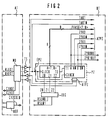
- the measuring logic ML shown in more detail in FIG. 2 is divided into an analog part AT and a digital part DT.
- the analog part AT comprising the measuring oscillator MO converts the capacitance to be measured, which is in each case coupled to the measuring oscillator MO by the switch unit S, into a square-wave signal.
- the square-wave signal clocks the period counter PZ, which is located in the digital part DT of the measuring logic ML.
- the period counter PZ counts the clocks generated by the measuring oscillator MO and controls the switch unit S via its two most significant bits.
- the voltage source REF can above all be used advantageously for reducing electrostatic interference forces on the movable center electrode if the first capacitance C1 and the second capacitance C2 are partial capacitances of a differential capacitor.
- connection C12COLD is connected to the ground points of the first capacitance C 1 and the second capacitance C 2 in order to minimize interfering electrostatic forces which can occur within the circuit arrangement.
- An external resistor can be connected to two connections RLEXT and RHEXT in order to control the charge / discharge current of the frequency-determining capacitors.
- the charge / discharge current can be increased by using the external resistor, whereby larger capacities can also be connected.
- FIG. 3 shows an embodiment of a rectangular generator RG, which can be provided in the circuit arrangement according to the invention.
- the task of the provided square-wave generator RG is merely to generate a frequency-variable square-wave signal, the frequency of the square-wave signal being dependent on the capacitance which is at the input ERG of the square-wave generator RG.
- the current switch SS can be modeled by two current sources of different polarity.
- the positive current source + I is activated and charges the capacitance, which is coupled to the square-wave generator RG via the switch unit S.
- the negated input signal Upn of the current switch SS is at low potential (0 volts).
- the input signal Up of the current switch SS switches to low potential (0 volt)
- the connected capacity is discharged via the negative current source -I.
- the negated input signal Upn of the current switch SS is high (5 volts).
- An output of the current switch SS is coupled to the switch unit S.
- the output of the current switch SS is also coupled to an input of the amplifier VS.
- An output of the amplifier VS is coupled to an input of the high-low level comparator HLK.
- a first output outn of the high-low level comparator HLK is coupled to a set input of the RS flip-flop RS.
- a second output out of the high-low level comparator HLK is coupled to a reset input of the RS flip-flop RS.
- a positive output Q of the RS flip-flop RS is fed back to a first input of the current switch SS and supplies the input signal Up of the current switch SS.
- This input signal Up of the current switch SS which is supplied by the RS flip-flop RS, provides at the same time represents a first clock signal TAKTN.
- a negated output QN of the RS flip-flop RS is connected to a second input of the current switch SS, at which the negated input signal Upn of the current switch SS is present.
- the negated input signal Upn of the current switch SS is supplied by the RS flip-flop RS and simultaneously represents a second clock signal CLOCK.
- the high-low-level comparator HLK has two comparators, a high-level comparator HK and a low-level comparator LK.
- the high-level comparator HK compares the applied triangle signal with a reference voltage level of preferably 3 volts and, if the applied triangle signal exceeds the reference voltage level, gives a low potential (0 volts) at the first output outn the high-low level. Comparator HVAC off, in the opposite case a high potential (5 volts).
- the low-level comparator LK works with a comparison potential of preferably 2 volts and an inverted output.
- the reference potential of the high-level comparator HK does not necessarily have to be 3 volts and the reference potential of the low-level comparator LK does not necessarily have to be 2 volts, but the reference potential can also assume other values.
- the output signals of the RS flip-flop RS are fed back to the inputs of the current switch SS.
- a period T of the resulting square-wave signal and thus also the time which the square-wave generator RG requires for N oscillations thus depends on the capacitance coupled to the square-wave generator RG by the switch unit S, in the case of the preferred exemplary embodiment even linear.
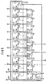
- the period counter PZ has a synchronously operating counter chain, as z. B. is described in Figure 5.
- the two most significant bits of the period counter PZ control the switch unit S and thus the selection of the capacitance to be measured.
- the period counter PZ thus represents a cycle counter.
- the period counter PZ can be designed variable in its bit width.
- the number N of cycles and thus the time per measuring cycle can be halved step by step.
- the number of pulses counted by an asynchronous counter AZ described later is also halved, which results in a reduction in the resolution of the measurement.
- this can be tolerated if the speed of the measurement is more important than the resolution of the measurement.
- the variation in the bit width of the period counter PZ is achieved in that a seventh bit is gradually synchronized with the preceding bits, as shown in FIG. Therefore, the partial factor N is halved, which results in a shorter measurement time at the expense of a reduced resolution.
- Control inputs Z0, Z1 and Z2 of the controllable logic gates N2 are reduced to two external control inputs RSLN0 and RSLN1 using the decoding stage DEC (cf. FIG. 2).
- Each sub-cycle which is described below, extends over a period of time which depends on the measured capacitance.
- the task of the evaluation logic AL is to assign a proportional binary value to the time period and from the obtained ones Values to calculate the capacitance difference between the first capacitance C1 and the second capacitance C2. This is done by measuring the time required for a sub-cycle using an RF clock.
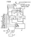
- FIG. 7 schematically describes the structure of the evaluation logic AL.
- the evaluation logic AL is divided into the control unit ST and an operation unit OW.
- the evaluation logic AL is implemented in digital form.
- evaluation logic AL can also be implemented in an analog form.
- the invention is not limited to a digital evaluation logic AL, but also includes an analog evaluation logic AL, the structure of which is known to any person skilled in the art.
- evaluation logic AL is made up of digital components.
- One advantage is the comparatively low hardware outlay for implementing the entire circuit arrangement.
- the control unit ST which, as described in FIG. 9, is divided into three sub-control units, takes over the coordination of the actions carried out in the operations unit OW.
- inputs of the control unit ST are coupled to the measurement logic ML.
- the assignment The inputs to the corresponding connections in the measurement logic ML can be recognized by the reference symbols shown in FIG. 7 and FIG.
- a first partial control unit TD of the control unit ST is responsible for controlling a dividing stage DVS, which is located in the operations unit OW (cf. FIG. 8).
- a second partial control unit TO controls any offset compensation that may be provided.
- a third sub-control unit TZ is used to control the asynchronous counter AZ, which is also located in the operation value K OW.
- the respective control signals are shown in FIG. 9 and in FIG. 8, which shows the various controls.
- An AND gate & is controlled with the aid of a D flip-flop FD1 and is coupled to an output of an HF oscillator HF via a second input.
- An output of the AND gate & is coupled to a counting input ZP of the asynchronous counter AZ.
- Any other counter which can process input signals of sufficiently high frequencies can of course also be used to implement the asynchronous counter AZ.
- the counting direction of the asynchronous counter AZ is determined by the third sub-control unit TZ via the signal UPDOWNN (cf. FIG. 9 and FIG. 10).
- the asynchronous counter AZ can also be pre-assigned with a specific start value.
- the default value consists of the negative difference between the first capacitance C 1 and the second capacitance C 2 . If no offset compensation is provided, the asynchronous counter AZ is preset with the value 0.
- three registers are also provided in the operational unit OW of the evaluation logic AL.
- An offset register OR is coupled to a data input DATA of the asynchronous counter AZ and to an output BC2MC2 of the subtracting stage SUB.
- the BC2MC2 output is also coupled to an BC1MC2 input of a dividing stage DVS.
- a sign output VZA of the subtracting stage SUB is coupled to a sign input VZE of the dividing stage DVS.
- a first register R1 is coupled to a second output A of the asynchronous counter AZ.
- the first register R1, in which the value of the first capacitance C 1 is stored, is coupled to a first input E1 of the subtracting stage SUB.
- a second input of the subtracting stage SUB is coupled to a second register R2 in which the total value of the first capacitance C 1 and the second capacitance C 2 , that is to say the value C 1 + C 2 , is stored.
- the second register R2 is also coupled to the second output A of the asynchronous counter AZ.
- the structure of the operational unit OW can also vary according to the variation of the method according to the invention used. Variations of the method according to the invention as well as the resulting variations of the operational work OW are described below.
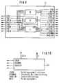
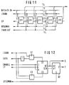
- the asynchronous counter AZ has a chain of 25 special toggle flip-flops connected in series, the structure of which is shown in FIG.
- FIG. 11 shows the special structure of the asynchronous counter AZ.
- the content of the offset register OR is read into the asynchronous counter AZ via the data input DATA with the leading edge of a LOADN signal.
- the UPDOWNN signal controls the counting direction of the asynchronous counter AZ.
- a signal ENABLEHF deactivates the asynchronous counter AZ during the change of counting direction to ensure that the current count remains unchanged when the counting direction is switched.
- the current counter reading of the asynchronous counter AZ can be queried at the second output A of the asynchronous counter AZ.
- a counter module ZFF used in the preferred embodiment in the asynchronous counter AZ, as shown in FIG. 12, has the following structure.
- a JK flip-flop is coupled to the signal ENABLEHF both with a first connection J and with a second connection K.
- a connection CD is coupled via a first OR gate O1, on the one hand, to a LOADN signal and, on the other hand, to the data line of the data input DATA of the asynchronous counter AZ, which in each case represents the location of the counter module within the asynchronous counter AZ.
- a connection SD of the JK flip-flop is coupled to a second OR gate O2, at the inputs of which there is the LOADN signal and the inverted signal which is present on the respective line of the DATA data input of the asynchronous counter AZ.
- the JK flip-flop is with one Output QZ coupled to a first input A0 of a multiplexer MP.
- a negated output QZN of the JK flip-flop is connected to a second input A1 of the multiplexer MP.
- One way to measure the difference in capacitance between the first capacitance C 1 and the second capacitance C 2 is e.g. B. in the method described below.
- the interference capacitance C P is measured in isolation by moving the switch unit S to the first switch position S1.
- all parasitic effects that can be modeled by an interference capacitance C P at the input ERG of the rectangular generator RG are measured in isolation in this switch position.
- the switch unit S remains in the first switch position S1 for the length of a first sub-cycle T1.
- Each sub-cycle that is controlled by the period counter PZ has the length of N clocks.
- the counting direction of the asynchronous counter AZ is set so that the asynchronous counter AZ counts down.
- the HF oscillator HF is switched through to the asynchronous counter AZ via the AND gate as soon as the switch unit S has selected a capacitance and the measuring oscillator MO has settled.
- Ensuring that the measuring oscillator is in a steady state can e.g. B. thereby achieved be that a period of the rectangular generator RG is simply waited until the HF oscillator HF is switched through to the asynchronous counter AZ. This measure eliminates switching errors.
- Other measures, e.g. B. another measure for determining the time until the RF oscillator HF is switched through to the asynchronous counter AZ are known to the person skilled in the art and can be implemented by a person skilled in the art without problems.
- the asynchronous counter AZ contains a value that represents the negative interference capacitance C P.
- a second sub-cycle T2 which also lasts for N cycles, the switch unit S is brought into the second switch position S2, as a result of which the disturbed first capacitor C 1 'is switched through to the square-wave generator RG.
- the disturbed first capacitance C 1 ' results from the sum of the first capacitance C 1 and the interference capacitance C P.
- the counting direction of the asynchronous counter AZ is set by the control unit ST so that the asynchronous counter AZ counts up.
- the output clock of the HF oscillator HF is switched through to the asynchronous counter AZ via the AND gate.
- the value representing the first capacitance C 1 is read out from the asynchronous counter AZ and multiplied by a factor of 2. This value is stored in the first register R1.
- the switch unit S is brought into the third switch position S3, as a result of which the disturbed second capacitance C 2 'is switched through to the square-wave generator RG.
- the counting direction of the asynchronous counter AZ is set so that the asynchronous counter AZ counts up.
- a fourth sub-cycle T4 the switch unit S is brought back to the first switch position S1, which in turn means that only the interference capacitance CP is measured in isolation.
- the value of the asynchronous counter AZ which now represents the sum of the first capacitance C 1 and the second capacitance C 2 , is stored in the second register R2.
- FIG. 15 shows how the term C. 1 - C. 2nd C. 1 + C. 2nd , which describes a relative capacitance difference between the first capacitance C 1 and the second capacitance C 2 , is simplified in comparison to the commonly used calculation method, as shown in FIG. 14.
- circuit arrangement according to the invention naturally also changes in accordance with such elementary changes to the method according to the invention.
- the circuit arrangement according to the invention thus extends not only to the preferred exemplary embodiment described.
- the negative difference between the two capacitances that is to say between the first capacitance C 1 and the second capacitance C 2 , is formed in the rest position. This value is then the numerator and denominator of the quotient C. 1 - C. 2nd C. 1 + C. 2nd deducted.
Landscapes
- Physics & Mathematics (AREA)
- General Physics & Mathematics (AREA)
- Measurement Of Resistance Or Impedance (AREA)
- Transmission And Conversion Of Sensor Element Output (AREA)
Applications Claiming Priority (2)
| Application Number | Priority Date | Filing Date | Title |
|---|---|---|---|
| DE19524387A DE19524387C1 (de) | 1995-07-04 | 1995-07-04 | Schaltungsanordnung und Verfahren zum Messen eines Kapazitätsunterschiedes zwischen einer ersten Kapazität C1 und einer zweiten Kapazität C2 |
| DE19524387 | 1995-07-04 |
Publications (2)
| Publication Number | Publication Date |
|---|---|
| EP0753756A2 true EP0753756A2 (fr) | 1997-01-15 |
| EP0753756A3 EP0753756A3 (fr) | 1999-05-12 |
Family
ID=7766012
Family Applications (1)
| Application Number | Title | Priority Date | Filing Date |
|---|---|---|---|
| EP96110443A Withdrawn EP0753756A3 (fr) | 1995-07-04 | 1996-06-27 | Circuit et procédé pour mesurer la différence de capacité entre deux capacités |
Country Status (3)
| Country | Link |
|---|---|
| US (1) | US5777482A (fr) |
| EP (1) | EP0753756A3 (fr) |
| DE (1) | DE19524387C1 (fr) |
Families Citing this family (11)
| Publication number | Priority date | Publication date | Assignee | Title |
|---|---|---|---|---|
| NO308333B2 (no) * | 1997-04-08 | 2000-08-28 | Sentech As | Anordning for kapasitiv elektrisk deteksjon eller maling |
| US5963043A (en) * | 1997-09-17 | 1999-10-05 | International Business Machines Corporation | Method and apparatus for characterized parasitic capacitance between integrated-circuit interconnects |
| DE19756963C1 (de) * | 1997-12-20 | 1999-09-23 | Reinhard Wiesemann | Verfahren und Vorrichtung zur Messung kleiner Kapazitäten oder kleiner Kapazitätsänderungen |
| US6731121B1 (en) | 1999-10-15 | 2004-05-04 | Microsensors Corp. | Highly configurable capacitive transducer interface circuit |
| JP4352562B2 (ja) * | 2000-03-02 | 2009-10-28 | 株式会社デンソー | 信号処理装置 |
| GB2385132A (en) * | 2002-02-12 | 2003-08-13 | Seiko Epson Corp | A capacitance sensor |
| JP4455201B2 (ja) * | 2004-07-20 | 2010-04-21 | 富士通マイクロエレクトロニクス株式会社 | 検出回路 |
| DE102006020301B4 (de) * | 2005-05-07 | 2014-07-31 | Acam-Messelectronic Gmbh | Verfahren und Vorrichtung zum Messen von Kapazitäten |
| US8688393B2 (en) * | 2010-07-29 | 2014-04-01 | Medtronic, Inc. | Techniques for approximating a difference between two capacitances |
| US8933712B2 (en) | 2012-01-31 | 2015-01-13 | Medtronic, Inc. | Servo techniques for approximation of differential capacitance of a sensor |
| JP6871836B2 (ja) * | 2017-09-29 | 2021-05-12 | 日本航空電子工業株式会社 | 容量検出装置、抵抗検出装置 |
Citations (9)
| Publication number | Priority date | Publication date | Assignee | Title |
|---|---|---|---|---|
| US3824459A (en) * | 1972-09-21 | 1974-07-16 | Iwatsu Electric Co Ltd | Method of measuring the electrostatic capacity of a capacitor |
| EP0136248A2 (fr) * | 1983-08-29 | 1985-04-03 | United Technologies Corporation | Circuit de conditionnement du signal d'un transducteur capacitif de pression |
| GB2159965A (en) * | 1984-05-31 | 1985-12-11 | Vaisala Oy | Method for the measurement of capacitance |
| EP0166705A2 (fr) * | 1984-05-31 | 1986-01-02 | Vaisala Oy | Méthode pour mesurer des capacités, particulièrement des capacités basses |
| EP0166706A1 (fr) * | 1984-05-31 | 1986-01-02 | Vaisala Oy | Méthode pour mesurer des capacités, en particulier des capacités basses |
| JPS61140834A (ja) * | 1984-12-13 | 1986-06-27 | Yokogawa Electric Corp | 圧力変換器 |
| GB2227847A (en) * | 1989-02-01 | 1990-08-08 | Gen Electric | Measuring electric power |
| EP0520352A2 (fr) * | 1991-06-22 | 1992-12-30 | Toyoda Koki Kabushiki Kaisha | Dispositif capteur capacitif |
| DE4313327A1 (de) * | 1993-04-23 | 1994-10-27 | Vdo Schindling | Anordnung zur Messung kleiner Kapazitäten |
Family Cites Families (4)
| Publication number | Priority date | Publication date | Assignee | Title |
|---|---|---|---|---|
| US4736629A (en) * | 1985-12-20 | 1988-04-12 | Silicon Designs, Inc. | Micro-miniature accelerometer |
| DE3919191C2 (de) * | 1989-06-13 | 1999-12-09 | Mannesmann Vdo Ag | Auswerteschaltung |
| FR2675583B1 (fr) * | 1991-04-18 | 1993-08-27 | Marelli Autronica | Procede et dispositif de mesure de condensateur. |
| DE19513022C1 (de) * | 1995-04-06 | 1996-08-14 | Siemens Ag | Schaltungsanordnung und Verfahren zur Bestimmung von Kapazitätsdifferenzen |
-
1995
- 1995-07-04 DE DE19524387A patent/DE19524387C1/de not_active Expired - Fee Related
-
1996
- 1996-06-27 EP EP96110443A patent/EP0753756A3/fr not_active Withdrawn
- 1996-07-03 US US08/675,590 patent/US5777482A/en not_active Expired - Lifetime
Patent Citations (9)
| Publication number | Priority date | Publication date | Assignee | Title |
|---|---|---|---|---|
| US3824459A (en) * | 1972-09-21 | 1974-07-16 | Iwatsu Electric Co Ltd | Method of measuring the electrostatic capacity of a capacitor |
| EP0136248A2 (fr) * | 1983-08-29 | 1985-04-03 | United Technologies Corporation | Circuit de conditionnement du signal d'un transducteur capacitif de pression |
| GB2159965A (en) * | 1984-05-31 | 1985-12-11 | Vaisala Oy | Method for the measurement of capacitance |
| EP0166705A2 (fr) * | 1984-05-31 | 1986-01-02 | Vaisala Oy | Méthode pour mesurer des capacités, particulièrement des capacités basses |
| EP0166706A1 (fr) * | 1984-05-31 | 1986-01-02 | Vaisala Oy | Méthode pour mesurer des capacités, en particulier des capacités basses |
| JPS61140834A (ja) * | 1984-12-13 | 1986-06-27 | Yokogawa Electric Corp | 圧力変換器 |
| GB2227847A (en) * | 1989-02-01 | 1990-08-08 | Gen Electric | Measuring electric power |
| EP0520352A2 (fr) * | 1991-06-22 | 1992-12-30 | Toyoda Koki Kabushiki Kaisha | Dispositif capteur capacitif |
| DE4313327A1 (de) * | 1993-04-23 | 1994-10-27 | Vdo Schindling | Anordnung zur Messung kleiner Kapazitäten |
Non-Patent Citations (1)
| Title |
|---|
| PATENT ABSTRACTS OF JAPAN vol. 10, no. 338 (P-516) [2394], 15. November 1986 & JP 61 140834 A (YOKOGAWA HOKUSHIN ELECTRIC CORP), 27. Juni 1986 * |
Also Published As
| Publication number | Publication date |
|---|---|
| US5777482A (en) | 1998-07-07 |
| DE19524387C1 (de) | 1996-11-07 |
| EP0753756A3 (fr) | 1999-05-12 |
Similar Documents
| Publication | Publication Date | Title |
|---|---|---|
| DE69500956T2 (de) | Schaltungsanordnung zur Signalgewinnung bei einem kapazitiven Differenzsensor | |
| EP0126846B1 (fr) | Capteur inductif | |
| DE10156027B4 (de) | Abgleichbare Filterschaltung | |
| DE19644125C2 (de) | Kapazitive Sensorschnittstellenschaltung | |
| DE19739532C2 (de) | Kapazitätssensor-Schnittstellenschaltung | |
| DE102006051365B4 (de) | Messverstärkungsvorrichtung und -verfahren | |
| EP0316616A2 (fr) | Convertisseur analogique-numérique | |
| DE3332152C2 (fr) | ||
| EP1419365A1 (fr) | Dispositif et procede de lecture d'un condensateur differentiel comportant un premier et un deuxieme condensateur partiel | |
| DE3633791A1 (de) | Verfahren und anordnung zur messung des widerstandsverhaeltnisses an einer widerstands-halbbruecke | |
| EP0753756A2 (fr) | Circuit et procédé pour mesurer la différence de capacité entre deux capacités | |
| EP0017251A1 (fr) | Dispositif de commutation pour déterminer la durée moyenne de la période d'un signal périodique | |
| DE3887593T2 (de) | Mehrfrequenz Kapazitäts-Sensor. | |
| DE2835133C2 (fr) | ||
| EP0356438A1 (fr) | Procede et dispositif pour evaluer une grandeur electrique analogique. | |
| DE69404977T2 (de) | Temperaturkorrigierter integrierender analog-digital-wandler | |
| EP0280261A2 (fr) | Circuit pour la production d'un signal carré indépendant de la température à une grandeur mesurée | |
| DE3639070A1 (de) | Verfahren zur messung des verhaeltnisses einer messgroessenabhaengigen kapazitaet zu einer referenzkapazitaet und einrichtung zur durchfuehrung des verfahrens | |
| DE69121756T2 (de) | Asynchrone Verzögerungsschaltung | |
| EP0444233A1 (fr) | Procédé et dispositif de conversion analogique/numérique d'un signal d'entrée analogique variant dans le temps | |
| EP0561054B1 (fr) | Appareil et procédé pour mesurer la constante de temps d'un capteur de déplacement | |
| DE3617936C2 (fr) | ||
| DE19703633C2 (de) | Verfahren zur Bestimmung eines Zeitintervalls zwischen zwei Ereignissen | |
| DE2363873A1 (de) | Anordnung zur dichtebestimmung | |
| EP0221402B1 (fr) | Convertisseur de grandeur analogique en fréquence |
Legal Events
| Date | Code | Title | Description |
|---|---|---|---|
| PUAI | Public reference made under article 153(3) epc to a published international application that has entered the european phase |
Free format text: ORIGINAL CODE: 0009012 |
|
| AK | Designated contracting states |
Kind code of ref document: A2 Designated state(s): DE FR GB IT SE |
|
| PUAL | Search report despatched |
Free format text: ORIGINAL CODE: 0009013 |
|
| AK | Designated contracting states |
Kind code of ref document: A3 Designated state(s): DE FR GB IT SE |
|
| 17P | Request for examination filed |
Effective date: 19990607 |
|
| RAP1 | Party data changed (applicant data changed or rights of an application transferred) |
Owner name: INFINEON TECHNOLOGIES AG |
|
| STAA | Information on the status of an ep patent application or granted ep patent |
Free format text: STATUS: THE APPLICATION HAS BEEN WITHDRAWN |
|
| 18W | Application withdrawn |
Withdrawal date: 20020114 |