EP0750335A2 - Poliermittel zur Polierung von Halbleiterscheiben und Verfahren zum Polieren unter Verwendung derselben - Google Patents
Poliermittel zur Polierung von Halbleiterscheiben und Verfahren zum Polieren unter Verwendung derselben Download PDFInfo
- Publication number
- EP0750335A2 EP0750335A2 EP96110070A EP96110070A EP0750335A2 EP 0750335 A2 EP0750335 A2 EP 0750335A2 EP 96110070 A EP96110070 A EP 96110070A EP 96110070 A EP96110070 A EP 96110070A EP 0750335 A2 EP0750335 A2 EP 0750335A2
- Authority
- EP
- European Patent Office
- Prior art keywords
- polishing
- wafer
- semiconductor wafer
- polishing agent
- back face
- Prior art date
- Legal status (The legal status is an assumption and is not a legal conclusion. Google has not performed a legal analysis and makes no representation as to the accuracy of the status listed.)
- Withdrawn
Links
Images


Classifications
-
- H—ELECTRICITY
- H10—SEMICONDUCTOR DEVICES; ELECTRIC SOLID-STATE DEVICES NOT OTHERWISE PROVIDED FOR
- H10P—GENERIC PROCESSES OR APPARATUS FOR THE MANUFACTURE OR TREATMENT OF DEVICES COVERED BY CLASS H10
- H10P52/00—Grinding, lapping or polishing of wafers, substrates or parts of devices
-
- H—ELECTRICITY
- H10—SEMICONDUCTOR DEVICES; ELECTRIC SOLID-STATE DEVICES NOT OTHERWISE PROVIDED FOR
- H10P—GENERIC PROCESSES OR APPARATUS FOR THE MANUFACTURE OR TREATMENT OF DEVICES COVERED BY CLASS H10
- H10P90/00—Preparation of wafers not covered by a single main group of this subclass, e.g. wafer reinforcement
- H10P90/12—Preparing bulk and homogeneous wafers
- H10P90/129—Preparing bulk and homogeneous wafers by polishing
-
- H—ELECTRICITY
- H10—SEMICONDUCTOR DEVICES; ELECTRIC SOLID-STATE DEVICES NOT OTHERWISE PROVIDED FOR
- H10P—GENERIC PROCESSES OR APPARATUS FOR THE MANUFACTURE OR TREATMENT OF DEVICES COVERED BY CLASS H10
- H10P52/00—Grinding, lapping or polishing of wafers, substrates or parts of devices
- H10P52/40—Chemomechanical polishing [CMP]
- H10P52/402—Chemomechanical polishing [CMP] of semiconductor materials
-
- Y—GENERAL TAGGING OF NEW TECHNOLOGICAL DEVELOPMENTS; GENERAL TAGGING OF CROSS-SECTIONAL TECHNOLOGIES SPANNING OVER SEVERAL SECTIONS OF THE IPC; TECHNICAL SUBJECTS COVERED BY FORMER USPC CROSS-REFERENCE ART COLLECTIONS [XRACs] AND DIGESTS
- Y10—TECHNICAL SUBJECTS COVERED BY FORMER USPC
- Y10T—TECHNICAL SUBJECTS COVERED BY FORMER US CLASSIFICATION
- Y10T428/00—Stock material or miscellaneous articles
- Y10T428/21—Circular sheet or circular blank
Definitions
- the present invention relates to a polishing agent and a polishing method used for polishing semiconductor wafers, in particular, single-crystal silicon wafers (hereinafter may be referred to, for brevity, as "wafer"). Further, this invention relates to a novel semiconductor wafer having a back face with an unconventional surface shape.
- the manufacturing method of semiconductor wafers includes a slicing process (A) to obtain wafers of thin disc type by slicing a single crystal ingot formed by a pulling process using a crystal pulling machine; a chamfering process (B) to chamfer a peripheral edge portion of the wafer obtained through the slicing process (A) to prevent cracking or breakage of the wafer; a lapping process (C) to flatten the surface of the chamfered wafer by lapping it; an etching process (D) to remove mechanical damage of the so chamfered and lapped wafer; a primary mirror polishing process (E1) to polish one side of the etched wafer to obtain a primary mirror surface of the wafer; a final mirror polishing process (G) to finally polish the surface of the so primary mirror polished wafer to obtain a final mirror surface of the wafer; and a washing process (H) for washing the finally mirror polished wafer to remove the polishing agent or dust particles from its surface.
- A slicing process
- etching process (D) there are two types of processes, that is, an acid etching process using an acid etching solution of a mixed acid or the like and an alkaline etching process using an alkaline etching solution of NaOH or the like.
- an acid etching process as shown in Fig. 11, a relatively high etching rate is obtained, and a surface roughness of an etched wafer is so fine that a cycle of the roughness is less than 10 ⁇ m and a P-V (Peak to Valley) value thereof is smaller than 0.6 ⁇ m.
- a surface roughness of an etched wafer is so large that a cycle of the roughness is in the range of 10 to 20 ⁇ m and a P-V value thereof sometimes exceeds 1.5 ⁇ m.
- the back face also becomes a mirror surface.
- respective sensors of processing machines can not distinguish the front face from the back face.
- the so mirror polished wafer tends to slip out from a conveying line.
- Another object of the present invention is to provide a semiconductor wafer polishing method using such novel polishing agnet for enabling novel low brightness polishing of the semi-conductor wafer.
- Still another object of the present invention is to provide a novel semiconductor wafer having a back face with an unconventional surface shape.
- the present invention seeks to provide a semiconductor wafer polishing agent which contains mainly a silica containing polishing agent and is added with a polyolefin type fine particle material.
- the silica containing polishing agent includes a colloidal silica polishing agent, and it is preferred to use a polyolefin aqueous dispersion as the polyolefin type fine particle material.
- the amount of the polyolefin type fine particle material is in the range of 0.01 to 1 percent by weight, preferably 0.01 to 0.5 percent by weight, and optimally 0.01 to 0.1 percent by weight relative to the total amount of the polishing agent.
- the polyolefin type fine particle material or polyolefin aqueous dispersion includes the aqueous dispersions disclosed in Japanese Patent Laid-open Publication Nos.4-46904, 4-88025 to 88026, 4-89830 to 89832 and 4-218548 to 218549. Further, it is preferred to use CHEMIPEARL (trade name for a polyolefin aqueous dispersion manufactured by Mitsui Petrochemical Industries, Ltd.) which contains the above noted polyolefin type fine particle material or polyolefin aqueous dispersion.
- CHEMIPEARL trade name for a polyolefin aqueous dispersion manufactured by Mitsui Petrochemical Industries, Ltd.
- the present invention seeks to provide a method of polishing a semiconductor wafer characterized by low brightness polishing using the above described semiconductor wafer polishing agent for polishing a semiconductor wafer.
- the present invention seeks to provide a semiconductor wafer characterized by having a mirror surface as the front face and a low brightness polished face, as the back face, formed by the above low brightness polishing method.
- the present invention seeks to provide a semiconductor wafer characterized in that the front face is a mirror surface and the back face has many semi-spherical small projections.
- the height of the projections is in the range of 0.05 to 0.5 ⁇ m, and the diameter thereof is in the range of 50 to 500 ⁇ m.
- the most important feature of the present invention is that low brightness polishing can be achieved by forming the semi-spherical small projections having a height of 50 to 500 ⁇ m and a diameter of 0.05 to 0.5 ⁇ m in the back face of a semiconductor wafer which is polished using a silica containing polishing agent added with a polyolefin type fine particle material. Accordingly, by mirror polishing the front face of the wafer and low brightness polishing the back face of the wafer, difference in brightness occurs between the front and back faces. Therefore, sensor detection of the front and back faces becomes possible.
- the term "brightness" denotes the percentage of the tested face reflectance relative to 100 of the perfect mirror surface reflectance.
- the use of the semiconductor wafer polishing agent of the present invention makes it possible to obtain a semiconductor wafer having a novel back face shape.
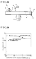
- Fig.8 shows an apparatus 10 for polishing a single crystal silicon wafer W, to carry out polishing processes in Experiment 1, Example 1 and Comparative Examples 1-3.
- the apparatus 10 comprises a rotary table assembly 12, a rotary wafer carrier 13, and a polishing agent supplying member 14.
- the rotary table assembly 12 comprises a rotary table 15 and a polishing pad 16 adhered on the upper surface of the rotary table 15.
- the rotary table 15 can rotate on a shaft 17 at a predetermined rotation speed by a driving device such as a motor.
- the rotary wafer carrier 13 is for holding with a vacuum chucking means or the like means to carry the wafer W on the polishing pad 16 of the rotary table assembly 12 so that the surface of the wafer W faces to the polishing pad 16.
- the wafer carrier 13 can rotate on a shaft 18 at a predetermined rotation speed and horizontally move on the polishing pad 16 by an appropriate driving device such as a motor.
- an appropriate driving device such as a motor.
- the wafer W held by the wafer carrier 13 is in contact with the polishing pad 16 and proper polishing loads are applied to the wafer W in a downward direction through the shaft 18 and the wafer carrier 13.
- the polishing agent supplying member 14 is for supplying a polishing agent 19 on the polishing pad 16 to supply it between the wafer W and the polishing pad 16.
- the amount (wt%) of the polyolefin type fine particle material was changed with 0.025, 0.1, 0.45 and 1.0. Also, the amount of pure water was changed for the total amount of the polishing agent so as to become 100 vol%.
- the polishing apparatus shown in Fig.8 the back face of each sample wafer (two sheets for each test) was polished to measure the polishing rate in the polishing process. The results of the measurement are shown in Fig.9.
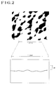
- Fig.1 is a photomicrograph of the back face of the sample wafer processed in Example 1.
- Fig.2 is a photomicrograph of another back face portion of the same sample wafer together with a graph showing the undulations in the back face measured by a surface roughness tester.
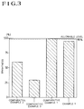
- the brightness of the back face of the sample wafer was measured.
- the results of the measurement are shown in Fig.3.
- Figs.1 and 2 semi-spherical small projections having a diameter of 50 to 500 ⁇ m and a height of 0.05 to 0.5 ⁇ m were formed. Also, as is seen from Fig.3, the brightness was 95% which led to the fact that the low brightness polishing could be achieved.
- a surface We for evaluation of the sample wafer W was pressed with load of 1 kg/cm 2 against a cleaned mirror surface Wm of a mirror surface wafer W1.
- the number of dust particles (the number of particles whose size was larger than 0.1 ⁇ m) on the cleaned mirror surface Wm transferred from the evaluation surface We of the sample wafer W onto the cleaned mirror surface Wm of the mirror surface wafer W1 was counted using a particle counter.
- the results of the couting are shown in Fig.4 in which the dust generation for the low brightness polished surface We of the sample wafer W was evaluated.
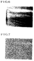
- Fig.6 is a photomicrograph of the surface of the mirror polished wafer. The brightness was measured in the same manner as in Example 1, and the results of the measurement are shown in Fig.3. Also, the evaluation on the dust generation was conducted in the same manner as in Example 1, and the results thereof are shown in Fig.4. As is clearly seen from Fig.6, undulations of large surface roughness on the mirror polished surface were not seen, and the brightness thereof was 100% as shown in Fig.3. The number of particles counted to evaluate the dust generation was about 200 which was extremely low.
- Fig.7 is a photomicrograph of the back face, that is, the acid etched surface of the sample wafer. As is apparent from Fig.7, undulations of fine roughness were formed on the back face of the wafer, a cycle of which was less than 10 ⁇ m and a P-V (Peak to Valley) value of which was smaller than 0.6 ⁇ m. Also, the brightness on the acid etched surface, that is, the back face of the sample wafer was measured, and the results of the measurement are shown in Fig.3.
- the dust generation for the acid etched surface or the back face was then evaluated in the same manner as in Example 1, and the results thereof are shown in Fig.4.
- the brightness of the acid etched surface was 60% which was lower than that in Example 1.
- the number of particles counted to evaluate the dust generation was about 700 which was quite higher than that obtained in Example 1.
- the polyolefin type fine particle material was added in the silica containing polishing agent.
- the same effect can be obtained even in case of adding agents, for example, ethylenediamine and the like which are usually added to the silica containing polishing agent.
- smooth semi-spherical projections can be formed on the back face of the wafer by polishing the face using the semiconductor wafer polishing agent of the present invention, thereby to lower the brightness of the back face of the wafer.
- sensor detection of the front and back faces of the wafer becomes possible, and the yield of semiconductor devices can be increased by suppressing the generation of dust to be caused by chipping on the back face of the wafer.
Landscapes
- Mechanical Treatment Of Semiconductor (AREA)
- Finish Polishing, Edge Sharpening, And Grinding By Specific Grinding Devices (AREA)
Applications Claiming Priority (2)
| Application Number | Priority Date | Filing Date | Title |
|---|---|---|---|
| JP181130/95 | 1995-06-23 | ||
| JP18113095A JP3134719B2 (ja) | 1995-06-23 | 1995-06-23 | 半導体ウェーハ研磨用研磨剤及び研磨方法 |
Publications (2)
| Publication Number | Publication Date |
|---|---|
| EP0750335A2 true EP0750335A2 (de) | 1996-12-27 |
| EP0750335A3 EP0750335A3 (de) | 1998-09-23 |
Family
ID=16095404
Family Applications (1)
| Application Number | Title | Priority Date | Filing Date |
|---|---|---|---|
| EP96110070A Withdrawn EP0750335A3 (de) | 1995-06-23 | 1996-06-21 | Poliermittel zur Polierung von Halbleiterscheiben und Verfahren zum Polieren unter Verwendung derselben |
Country Status (4)
| Country | Link |
|---|---|
| US (2) | US5866226A (de) |
| EP (1) | EP0750335A3 (de) |
| JP (1) | JP3134719B2 (de) |
| KR (1) | KR100203340B1 (de) |
Cited By (1)
| Publication number | Priority date | Publication date | Assignee | Title |
|---|---|---|---|---|
| EP1283551A3 (de) * | 2001-08-08 | 2004-07-28 | Shin-Etsu Chemical Co., Ltd. | Eckige Substrate |
Families Citing this family (12)
| Publication number | Priority date | Publication date | Assignee | Title |
|---|---|---|---|---|
| DE19722679A1 (de) * | 1997-05-30 | 1998-12-03 | Wacker Siltronic Halbleitermat | Scheibenhalter und Verfahren zur Herstellung einer Halbleiterscheibe |
| JP3449459B2 (ja) | 1997-06-02 | 2003-09-22 | 株式会社ジャパンエナジー | 薄膜形成装置用部材の製造方法および該装置用部材 |
| US6214704B1 (en) | 1998-12-16 | 2001-04-10 | Memc Electronic Materials, Inc. | Method of processing semiconductor wafers to build in back surface damage |
| KR20010004982A (ko) * | 1999-06-30 | 2001-01-15 | 김영환 | 반도체 소자의 산화막 연마용 슬러리 제조 방법 |
| JP2001267273A (ja) | 2000-01-11 | 2001-09-28 | Sumitomo Chem Co Ltd | 金属用研磨材、研磨組成物及び研磨方法 |
| CN1446142A (zh) * | 2000-08-07 | 2003-10-01 | Memc电子材料有限公司 | 用双面抛光加工半导体晶片的方法 |
| US20040108297A1 (en) * | 2002-09-18 | 2004-06-10 | Memc Electronic Materials, Inc. | Process for etching silicon wafers |
| US7456105B1 (en) * | 2002-12-17 | 2008-11-25 | Amd, Inc. | CMP metal polishing slurry and process with reduced solids concentration |
| JP4273943B2 (ja) * | 2003-12-01 | 2009-06-03 | 株式会社Sumco | シリコンウェーハの製造方法 |
| KR101618273B1 (ko) * | 2008-04-29 | 2016-05-04 | 세미퀘스트, 인코포레이티드 | 연마 패드 조성물, 및 이의 제조 방법 및 용도 |
| EP2349415B1 (de) | 2008-11-07 | 2020-01-01 | Becton, Dickinson and Company | Kanülengehäuse zur einfachen arzneimittelinjektion |
| CN110473774A (zh) * | 2019-08-23 | 2019-11-19 | 大同新成新材料股份有限公司 | 一种芯片硅生产用无尘加工工艺 |
Family Cites Families (13)
| Publication number | Priority date | Publication date | Assignee | Title |
|---|---|---|---|---|
| JPS54110783A (en) * | 1978-02-20 | 1979-08-30 | Hitachi Ltd | Semiconductor substrate and its manufacture |
| JPS6154614A (ja) * | 1984-08-24 | 1986-03-18 | Sumitomo Electric Ind Ltd | 化合物半導体基板の前処理方法 |
| US5352277A (en) * | 1988-12-12 | 1994-10-04 | E. I. Du Pont De Nemours & Company | Final polishing composition |
| JPH04291723A (ja) * | 1991-03-20 | 1992-10-15 | Asahi Denka Kogyo Kk | シリコンウェハー用研摩剤 |
| JPH04291724A (ja) * | 1991-03-20 | 1992-10-15 | Asahi Denka Kogyo Kk | シリコンウェハーの研摩方法 |
| JPH04291722A (ja) * | 1991-03-20 | 1992-10-15 | Asahi Denka Kogyo Kk | シリコンウェハー表面のヘイズ防止方法 |
| US5139571A (en) * | 1991-04-24 | 1992-08-18 | Motorola, Inc. | Non-contaminating wafer polishing slurry |
| US5264010A (en) * | 1992-04-27 | 1993-11-23 | Rodel, Inc. | Compositions and methods for polishing and planarizing surfaces |
| JP2839801B2 (ja) * | 1992-09-18 | 1998-12-16 | 三菱マテリアル株式会社 | ウェーハの製造方法 |
| JP2910507B2 (ja) * | 1993-06-08 | 1999-06-23 | 信越半導体株式会社 | 半導体ウエーハの製造方法 |
| JPH0786289A (ja) * | 1993-07-22 | 1995-03-31 | Toshiba Corp | 半導体シリコンウェハおよびその製造方法 |
| JP2894208B2 (ja) * | 1994-06-02 | 1999-05-24 | 信越半導体株式会社 | シリコンウェーハ研磨用研磨剤及び研磨方法 |
| JP3317330B2 (ja) * | 1995-12-27 | 2002-08-26 | 信越半導体株式会社 | 半導体鏡面ウェーハの製造方法 |
-
1995
- 1995-06-23 JP JP18113095A patent/JP3134719B2/ja not_active Expired - Fee Related
-
1996
- 1996-05-31 KR KR1019960019069A patent/KR100203340B1/ko not_active Expired - Fee Related
- 1996-06-20 US US08/670,258 patent/US5866226A/en not_active Expired - Fee Related
- 1996-06-21 EP EP96110070A patent/EP0750335A3/de not_active Withdrawn
-
1997
- 1997-08-21 US US08/915,579 patent/US5891353A/en not_active Expired - Fee Related
Cited By (2)
| Publication number | Priority date | Publication date | Assignee | Title |
|---|---|---|---|---|
| EP1283551A3 (de) * | 2001-08-08 | 2004-07-28 | Shin-Etsu Chemical Co., Ltd. | Eckige Substrate |
| US7122280B2 (en) | 2001-08-08 | 2006-10-17 | Shin-Etsu Chemical Co., Ltd. | Angular substrates |
Also Published As
| Publication number | Publication date |
|---|---|
| JP3134719B2 (ja) | 2001-02-13 |
| KR100203340B1 (ko) | 1999-06-15 |
| EP0750335A3 (de) | 1998-09-23 |
| KR970003588A (ko) | 1997-01-28 |
| JPH097987A (ja) | 1997-01-10 |
| US5866226A (en) | 1999-02-02 |
| US5891353A (en) | 1999-04-06 |
Similar Documents
| Publication | Publication Date | Title |
|---|---|---|
| US5821167A (en) | Method of manufacturing semiconductor mirror wafers | |
| JP5557506B2 (ja) | 半導体ウェーハの両面をポリッシングする方法 | |
| KR100299008B1 (ko) | 웨이퍼의제조방법 | |
| US5866226A (en) | Polishing agent used for polishing semiconductor wafers and polishing method using the same | |
| EP0754785B1 (de) | Verfahren zur Herstellung von Halbleiterscheiben mit spiegelglatter Oberfläche | |
| US6709981B2 (en) | Method and apparatus for processing a semiconductor wafer using novel final polishing method | |
| JP5628224B2 (ja) | 基板表面を研磨するための方法 | |
| KR100394972B1 (ko) | 에피택셜 코팅 반도체웨이퍼 및 그 제조방법 | |
| JP3004891B2 (ja) | 表面粗さを減少させるための半導体ウエハの粗研磨法 | |
| US6793837B2 (en) | Process for material-removing machining of both sides of semiconductor wafers | |
| US6861360B2 (en) | Double-sided polishing process for producing a multiplicity of silicon semiconductor wafers | |
| EP1005069A2 (de) | Halbleiterscheibe und Verfahren zu ihrer Herstellung | |
| JP4835069B2 (ja) | シリコンウェーハの製造方法 | |
| KR20000017512A (ko) | 웨이퍼 기판 재생방법 및 웨이퍼 기판 재생을 위한 연마액 조성물 | |
| US5827395A (en) | Polishing pad used for polishing silicon wafers and polishing method using the same | |
| KR102117362B1 (ko) | 실리콘 웨이퍼의 연마 방법 및 실리콘 웨이퍼의 제조 방법 | |
| GB2368971A (en) | Semiconductor wafer reclaim process | |
| EP1155777A1 (de) | Polierverfahren und -vorrichtung | |
| JP3447477B2 (ja) | 半導体基板を研磨する方法 | |
| JP4085356B2 (ja) | 半導体ウェーハの洗浄乾燥方法 | |
| KR20020017910A (ko) | 재생웨이퍼를 반도체웨이퍼로 변환시키는 방법 | |
| US20020115294A1 (en) | Epitaxial semiconductor wafer manufacturing method | |
| KR100792066B1 (ko) | 반도체 웨이퍼의 평탄화 가공방법 | |
| EP0685877A2 (de) | Poliermittel zur Polierung von Siliziumscheiben und Verfahren zum Polieren unter Verwendung desselben | |
| EP1129821A1 (de) | Verfahren und vorrichtung zum polieren von halbleiterscheiben |
Legal Events
| Date | Code | Title | Description |
|---|---|---|---|
| PUAI | Public reference made under article 153(3) epc to a published international application that has entered the european phase |
Free format text: ORIGINAL CODE: 0009012 |
|
| AK | Designated contracting states |
Kind code of ref document: A2 Designated state(s): DE FR GB |
|
| PUAL | Search report despatched |
Free format text: ORIGINAL CODE: 0009013 |
|
| AK | Designated contracting states |
Kind code of ref document: A3 Designated state(s): DE FR GB |
|
| 17P | Request for examination filed |
Effective date: 19990107 |
|
| 17Q | First examination report despatched |
Effective date: 19990702 |
|
| STAA | Information on the status of an ep patent application or granted ep patent |
Free format text: STATUS: THE APPLICATION IS DEEMED TO BE WITHDRAWN |
|
| 18D | Application deemed to be withdrawn |
Effective date: 20040103 |