EP0747713A2 - Circuit for measuring the load current of a power semiconductor device with a load on the source or drain side - Google Patents
Circuit for measuring the load current of a power semiconductor device with a load on the source or drain side Download PDFInfo
- Publication number
- EP0747713A2 EP0747713A2 EP96108434A EP96108434A EP0747713A2 EP 0747713 A2 EP0747713 A2 EP 0747713A2 EP 96108434 A EP96108434 A EP 96108434A EP 96108434 A EP96108434 A EP 96108434A EP 0747713 A2 EP0747713 A2 EP 0747713A2
- Authority
- EP
- European Patent Office
- Prior art keywords
- semiconductor component
- circuit arrangement
- source
- mosfet
- resistor
- Prior art date
- Legal status (The legal status is an assumption and is not a legal conclusion. Google has not performed a legal analysis and makes no representation as to the accuracy of the status listed.)
- Granted
Links
Images

Classifications
-
- G—PHYSICS
- G01—MEASURING; TESTING
- G01R—MEASURING ELECTRIC VARIABLES; MEASURING MAGNETIC VARIABLES
- G01R19/00—Arrangements for measuring currents or voltages or for indicating presence or sign thereof
-
- G—PHYSICS
- G05—CONTROLLING; REGULATING
- G05F—SYSTEMS FOR REGULATING ELECTRIC OR MAGNETIC VARIABLES
- G05F3/00—Non-retroactive systems for regulating electric variables by using an uncontrolled element, or an uncontrolled combination of elements, such element or such combination having self-regulating properties
- G05F3/02—Regulating voltage or current
- G05F3/08—Regulating voltage or current wherein the variable is DC
- G05F3/10—Regulating voltage or current wherein the variable is DC using uncontrolled devices with non-linear characteristics
- G05F3/16—Regulating voltage or current wherein the variable is DC using uncontrolled devices with non-linear characteristics being semiconductor devices
- G05F3/20—Regulating voltage or current wherein the variable is DC using uncontrolled devices with non-linear characteristics being semiconductor devices using diode- transistor combinations
- G05F3/24—Regulating voltage or current wherein the variable is DC using uncontrolled devices with non-linear characteristics being semiconductor devices using diode- transistor combinations wherein the transistors are of the field-effect type only
-
- G—PHYSICS
- G01—MEASURING; TESTING
- G01R—MEASURING ELECTRIC VARIABLES; MEASURING MAGNETIC VARIABLES
- G01R1/00—Details of instruments or arrangements of the types included in groups G01R5/00 - G01R13/00 and G01R31/00
- G01R1/20—Modifications of basic electric elements for use in electric measuring instruments; Structural combinations of such elements with such instruments
- G01R1/203—Resistors used for electric measuring, e.g. decade resistors standards, resistors for comparators, series resistors, shunts
-
- G—PHYSICS
- G01—MEASURING; TESTING
- G01R—MEASURING ELECTRIC VARIABLES; MEASURING MAGNETIC VARIABLES
- G01R19/00—Arrangements for measuring currents or voltages or for indicating presence or sign thereof
- G01R19/0092—Measuring current only
-
- H—ELECTRICITY
- H03—ELECTRONIC CIRCUITRY
- H03K—PULSE TECHNIQUE
- H03K17/00—Electronic switching or gating, i.e. not by contact-making and –breaking
- H03K17/14—Modifications for compensating variations of physical values, e.g. of temperature
- H03K17/145—Modifications for compensating variations of physical values, e.g. of temperature in field-effect transistor switches
-
- H—ELECTRICITY
- H03—ELECTRONIC CIRCUITRY
- H03K—PULSE TECHNIQUE
- H03K2217/00—Indexing scheme related to electronic switching or gating, i.e. not by contact-making or -breaking covered by H03K17/00
- H03K2217/0027—Measuring means of, e.g. currents through or voltages across the switch
Definitions
- the prerequisite is that the measuring resistor is matched to the load. With a different load, either the measuring resistance must be changed or the evaluation logic that detects the voltage.
- the invention has for its object to develop a circuit of the type mentioned so that it can be used regardless of the size of the load. In addition, it should be usable for the most common case of the "high-side" switch.
- the resistor is connected on the one hand to a terminal which is at a fixed potential and on the other hand via a controllable resistor to the source terminal of the further semiconductor component, and in that the current of the further semiconductor component is set by the controllable resistor in such a way that the drain -Source voltages of both semiconductor components are equal to one another.
- the circuit according to FIG. 1 contains a power MOSFET 1 to which a load 4 is connected in series on the source side. It therefore represents a high-side switch.
- the circuit also contains a further MOSFET 2.
- the drain connections D of both MOSFETs are connected to one another, as are their gate connections. Your source connections are separated.
- a controllable resistor 6 is connected to the source terminal of the MOSFET 2.
- the controllable resistor on the other hand, is connected to a measuring resistor 5 via a connection 10.
- the other connection of the measuring resistor 5 is at a fixed potential, preferably to ground. This mass can, but does not have to be identical to that on which the load 4 lies.
- the controllable resistor 6 is expediently designed as a MOSFET. Then its source connection is connected to the measuring resistor 5 and its drain connection to the source connection of the MOSFET 2. It is of the reverse channel type as the MOSFET 2. The gate connection of the MOSFET 6 is connected to the output of a differential amplifier 3. This has two inputs, of which the negative input is connected to the source terminal of the MOSFET 2 and the positive input is connected to the source terminal of the power MOSFET 1.
- the entire arrangement is based on an operating voltage + V bb , which is applied between a terminal 11 and ground.
- the connection 11 is connected to the drain connections of the MOSFET 1 and 2.
- the gate connections of both MOSFETs are connected via a resistor 8 to an input 9, to which a control voltage can be applied, for example via a pump circuit.
- the drain-source voltage at the power MOSFET 1 increases or decreases and thus the variable resistor 6 is controlled in the direction of lower or higher resistance until the voltage difference at the input of the amplifier 3 is zero.
- a prerequisite for the fixed proportionality is that the I D / U DS characteristics of MOSFET 1 and 2 are similar to each other. Ie that for each voltage value U DS a current flows through the further FET 2, which is a fixed fraction of the load current. At the resistor 5, this current generates a voltage which is related to ground and is proportional to the load current and which can be tapped at the terminal 10.
- the similarity can easily be achieved in that, as mentioned at the beginning, the MOSFET 2 is formed by some cells of the power MOSFET 1.
- the ratio can be, for example, 10: 10,000.
- the circuit arrangement according to FIG. 2 differs from that according to FIG. 1 by an additional differential amplifier 14, the first input of which is connected to the source connection of the power MOSFET 1.
- a fixed voltage is present at the other input of the differential amplifier 14.
- the output of 14 is connected to the gate terminals of MOSFET 1 and 2.
- the increase in the drain-source voltage at the MOSFET 1 by, for example, 0.1 V increases the on-state resistance of the power MOSFET only insignificantly. The increase in losses in power MOSFET 1 is thus negligible.
- the negative input of the amplifier 3 is connected to the terminal 11 via a diode 15 and to ground via a current source 18.
- the other output is connected to terminal 11 via a diode 16 and to ground via a current source 20.
- the negative input is also connected via a diode 17 to the source terminal of the MOSFET 2, the positive input via a diode 19 to the source terminal of the power MOSFET 1.
- the diodes and current sources serve to set the amplifier 3 to the correct operating point. All diodes can be designed as MOS diodes, the current sources can be implemented as a current mirror circuit or as a depletion MOSFET.
- a resistor 21 may be connected between the output of the amplifier 3 and the gate connection of the MOSFET 6, the connection of which is connected to the cat connection of 6 and connected to a capacitor 22.
- the other connection of the capacitor is grounded.
- This RC combination counteracts the tendency of amplifier 3 to oscillate.
- the amplifier 3 is expediently an operational amplifier.
- the circuit according to the invention can be operated essentially independently of temperature if the measuring resistor 5 itself is independent of temperature or not very dependent on temperature. This can e.g. can be achieved in that the measuring resistor 5 consists of polysilicon or is designed as a temperature-compensated resistor.
- the invention was explained using a high-side switch. However, it can also be used for a low-side switch.
- the load 4 is located on the drain side of the two MOSFETs, while the controllable switch 6 and the measuring resistor 5 remain connected on the source side of the MOSFET 2.
Landscapes
- Physics & Mathematics (AREA)
- Engineering & Computer Science (AREA)
- General Physics & Mathematics (AREA)
- Microelectronics & Electronic Packaging (AREA)
- Nonlinear Science (AREA)
- Electromagnetism (AREA)
- Radar, Positioning & Navigation (AREA)
- Automation & Control Theory (AREA)
- Measurement Of Current Or Voltage (AREA)
- Amplifiers (AREA)
- Testing Of Individual Semiconductor Devices (AREA)
- Control Of Voltage And Current In General (AREA)
Abstract
Ausgehend von dem bekannten Prinzip des "Sense"-FET wird zwischen dem Meßausgang und einem an Masse liegenden Meßwiderstand (5) ein steuerbarer Widerstand (6) angeschlossen. Sein Widerstandswert wird immer so eingestellt, daß die Drain-Sourcespannungen von Leistungs-FET einander (1)und "Sense"-FET (2) gleich sind. Damit wird erreicht, daß der Meßstrom dem Laststrom unabhängig von der Größe der Last proportional ist.
Description
Die Erfindung bezieht sich auf eine Schaltungsanordnung zum Erfassen des Laststroms eines durch Feldeffekt steuerbaren Leistungs-Halbleiterbauelements, mit den Merkmalen:
- einem weiteren durch Feldeffekt steuerbaren Halbleiterbauelement,
- die Drainanschlüsse und Gateanschlüsse beider Halbleiterbauelemente sind jeweils miteinander verbunden,
- durch das weitere Halbleiterbauelement fließt ein Bruchteil des Laststroms,
- einem dem weiteren Halbleiterbauelement in Reihe geschalteten Widerstand, an dem eine dem Laststrom proportionale Spannung abgreifbar ist.
- another semiconductor component controllable by field effect,
- the drain connections and gate connections of both semiconductor components are each connected to one another,
- a fraction of the load current flows through the further semiconductor component,
- a resistor connected in series with the further semiconductor component, from which a voltage proportional to the load current can be tapped.
Eine solche Schaltungsanordnung ist z.B. in dem Artikel "Surviving Short Circuits" von R.Frank und A.Pshaenich, Machine Design, March 8, 1990, Seiten 89 bis 96 beschrieben worden. In diesem Artikel ist das Prinzip dargestellt, daß der Laststrom eines Leistungs-MOSFET dadurch erfaßt werden kann, daß dem Leistungs-MOSFET ein ähnlicher, von der Fläche her kleinerer MOSFET parallel geschaltet und diesem kleineren MOSFET, dem sogenannten "Sense"-FET, sourceseitig ein Meßwiderstand in Reihe geschaltet wird. Ist der Leistungs-FET drainseitig mit einer Last verbunden, so fließt durch den weiteren FET ein Strom, der dem Laststrom etwa proportional ist. Der Proportionalitätsfaktor hängt dabei vom Verhältnis der stromführenden Flächen des Sense-FET zu der des Leistungs-FET ab. Fließt durch die Last und damit durch den Leistungs-FET ein Laststrom, so fließt damit ein dem Laststrom etwa proportionaler Teil durch den Sense-FET und den Meßwiderstand. Am Meßwiderstand kann dann eine dem Laststrom etwa proportionale Spannung abgegriffen werden.Such a circuit arrangement has been described, for example, in the article "Surviving Short Circuits" by R. Frank and A. Pshaenich, Machine Design, March 8, 1990, pages 89 to 96. In this article, the principle is presented that the load current of a power MOSFET can be detected by connecting the power MOSFET with a similar, smaller in area MOSFET in parallel and this smaller MOSFET, the so-called "sense" FET, on the source side a measuring resistor is connected in series. If the power FET is connected to a load on the drain side, a current flows through the further FET which is approximately proportional to the load current. The proportionality factor depends on the ratio of the current-carrying areas of the sense FET to that of the power FET. If a load current flows through the load and thus through the power FET, a part that is approximately proportional to the load current flows through the sense FET and the measuring resistor. A voltage approximately proportional to the load current can then be tapped at the measuring resistor.
Voraussetzung ist dabei, daß der Meßwiderstand auf die Last abgestimmt ist. Bei einer anderen Last muß daher entweder der Meßwiderstand geändert werden oder die die Spannung erfassende Auswertelogik.The prerequisite is that the measuring resistor is matched to the load. With a different load, either the measuring resistance must be changed or the evaluation logic that detects the voltage.
Der Erfindung liegt die Aufgabe zugrunde, eine Schaltung der erwähnten Gattung so weiterzubilden, daß sie unabhängig von der Größe der Last brauchbar ist. Außerdem soll sie für den meist vorkommenden Fall des "High-Side"-Schalters verwendbar sein.The invention has for its object to develop a circuit of the type mentioned so that it can be used regardless of the size of the load. In addition, it should be usable for the most common case of the "high-side" switch.
Diese Aufgabe wird dadurch gelöst, daß der Widerstand einerseits mit einem auf festem Potential liegenden Anschluß verbunden ist und andererseits über einen steuerbaren Widerstand mit dem Sourceanschluß des weiteren Halbleiterbauelementes, und daß der Strom des weiteren Halbleiterbauelementes durch den steuerbaren Widerstand derart eingestellt wird, daß die Drain-Sourcespannungen beider Halbleiterbauelemente einander gleich sind.This object is achieved in that the resistor is connected on the one hand to a terminal which is at a fixed potential and on the other hand via a controllable resistor to the source terminal of the further semiconductor component, and in that the current of the further semiconductor component is set by the controllable resistor in such a way that the drain -Source voltages of both semiconductor components are equal to one another.
Wird die Schaltungsanordnung nicht mit Leistungs-MOSFET sondern mit IGBT betrieben, so ist der Begriff "Source" durch "Emitter" zu ersetzen.If the circuit arrangement is operated not with power MOSFET but with IGBT, the term "source" is to be replaced by "emitter".
Weiterbildungen der Erfindung sind Gegenstand der Unteransprüche.Developments of the invention are the subject of the dependent claims.
Die Erfindung wird anhand dreier Ausführungsbeispiele in Verbindung mit den Figuren 1 bis 3 näher erläutert. Es zeigen:
Figur 1- den prinzipiellen Aufbau der Schaltungsanordnung,
Figur 2- eine erweiterte Schaltungsanordnung und
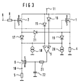
- Figur 3
- ein Ausführungsbeispiel, das gegenüber dem nach
Figur 1 durch verschiedene Komponenten ergänzt ist.
- Figure 1
- the basic structure of the circuit arrangement,
- Figure 2
- an extended circuit arrangement and
- Figure 3
- an embodiment which is supplemented by various components compared to that of Figure 1.
Die Schaltung nach Figur 1 enthält einen Leistungs-MOSFET 1, dem sourceseitig eine Last 4 in Reihe geschaltet ist. Er stellt damit einen High-Side-Schalter dar. Die Schaltung enthält außerdem einen weiteren MOSFET 2. Dieser bildet den erwähnten Sense-FET und ist im allgemeinen durch einige Zellen des Leistungs-MOSFET 1 gebildet. Er kann z.B. 10 Zellen umfassen, während der Leistungs-MOSFET 1 10000 Zellen hat. Die Drainanschlüsse D beider MOSFET sind miteinander verbunden, ebenso ihre Gateanschlüsse. Ihre Sourceanschlüsse sind getrennt. Mit dem Sourceanschluß des MOSFET 2 ist ein steuerbarer Widerstand 6 angeschlossen. Der steuerbare Widerstand ist andererseits über einen Anschluß 10 mit einem Meßwiderstand 5 verbunden. Der andere Anschluß des Meßwiderstandes 5 liegt an einem festen Potential, vorzugsweise an Masse. Diese Masse kann, muß jedoch jedoch nicht derjenigen identisch sein, an der die Last 4 liegt.The circuit according to FIG. 1 contains a
Der steuerbare Widerstand 6 ist zweckmäßigerweise als MOSFET ausgebildet. Dann ist sein Sourceanschluß mit dem Meßwiderstand 5 verbunden und sein Drainanschluß mit dem Sourceanschluß des MOSFET 2. Er ist vom umgekehrten Kanaltyp wie der MOSFET 2. Der Gateanschluß des MOSFET 6 ist mit dem Ausgang eines Differenzverstärkers 3 verbunden. Dieser hat zwei Eingänge, von denen der negative Eingang mit dem Sourceanschluß des MOSFET 2 und der positive Eingang mit dem Sourceanschluß des Leistungs-MOSFET 1 verbunden ist.The
Die gesamte Anordnung liegt an einer Betriebsspannung +Vbb, die zwischen einem Anschluß 11 und Masse angelegt wird. Der Anschluß 11 ist mit den Drainanschlüssen der MOSFET 1 und 2 verbunden. Die Gateanschlüsse beider MOSFET sind über einen Widerstand 8 mit einem Eingang 9 verbunden, an den, z.B. über eine Pumpschaltung eine Steuerspannung angelegt werden kann.The entire arrangement is based on an operating voltage + V bb , which is applied between a
Wird eine Steuerspannung am Eingang 9 angelegt, so wird der Leistungs-MOSFET 1 und der weitere MOSFET 2 leitend gesteuert. Es fließt ein Laststrom durch die Last 4. Durch den MOSFET 2, den steuerbaren Widerstand 6 und den Meßwiderstand 5 fließt ebenfalls ein Strom. An den Sourceanschlüssen der MOSFET 1 und 2 stellt sich jeweils eine Spannung ein, die am negativen bzw. positiven Eingang des Differenzverstärkers 3 anliegt. Abhängig von der Differenz dieser Spannungen tritt am Ausgang von 3 eine Spannung auf, die den MOSFET 6 steuert.If a control voltage is applied to the
Es sei zunächst angenommen, daß die Source-Drainspannung am MOSFET 2 größer ist als die am MOSFET 1. Dann tritt am Eingang des Differenzverstärkers 3 eine Spannung auf, die den MOSFET 6 in einen Bereich höheren Widerstandes steuert. Der Strom durch den MOSFET 2 wird dadurch verringert, wodurch seine Drain-Sourcespannung steigt. Der Strom durch den MOSFET 2 wird nun so lange geregelt, bis die Differenz der Eingangsspannungen Null ist, d.h. bis die Drain-Sourcespannungen der MOSFET 1 und 2 gleich sind. Das bedeutet, daß im eingeregelten, stationären Zustand durch den Meßwiderstand 5 ein Strom fließt, der dem Laststrom unabhängig von der Größe der Last 4 immer fest proportional ist. Ändert sich also im Lauf des Betriebes die Last 4 z.B. durch einen teilweisen Kurzschluß oder durch den Ausfall einiger parallelgeschalteter Lasten, so erhöht bzw. verringert sich die Drain-Sourcespannung am Leistungs-MOSFET 1 und damit wird der veränderbare Widerstand 6 in Richtung geringeren bzw. höheren Widerstandes gesteuert, bis die Spannungsdifferenz am Eingang des Verstärkers 3 Null ist.It is initially assumed that the source-drain voltage at the
Voraussetzung für die feste Proportionalität ist, daß die ID/UDS-Kennlinien der MOSFET 1 und 2 einander ähnlich sind. D.h., daß für jeden Spannungswert UDS durch den weiteren FET 2 ein Strom fließt, der einem festen Bruchteil des Laststroms beträgt. Dieser Strom erzeugt am Widerstand 5 eine auf Masse bezogene, dem Laststrom proportionale Spannung, die am Anschluß 10 abgegriffen werden kann. Die Ähnlichkeit läßt sich ohne weiteres erzielen, daß, wie eingangs erwähnt, der MOSFET 2 durch einige Zellen des Leistungs-MOSFET 1 gebildet ist. Das Verhältnis kann z.B. 10:10000 sein.A prerequisite for the fixed proportionality is that the I D / U DS characteristics of
Sind die Kennlinien einander nicht ähnlich, tritt ein vom Laststrom abhängiger Regelfehler auf.If the characteristic curves are not similar to one another, a control error that depends on the load current occurs.
Die Schaltungsanordnung nach Figur 2 unterscheidet sich von der nach Figur 1 durch einen zusätzlichen Differenzverstärker 14, dessen erster Eingang mit dem Sourceanschluß des Leistungs-MOSFET 1 verbunden ist. Am anderen Eingang des Differenzverstärkers 14 liegt eine feste Spannung an. Der Ausgang von 14 ist mit den Gateanschlüssen der MOSFET 1 und 2 verbunden. Der zusätzliche Differenzverstärker 14 hat den Zweck, die Drain-Sourcespannung des MOSFET 1 auf einen Wert einzustellen, der höher ist als die Offset-Spannung des Differenzverstärkers 3. Beträgt die Offset-Spannung z.B. 5 mV, so kann die am zweiten Eingang des Verstärkers 14 liegende Spannung z.B. Vbb-0,1 V sein. Damit wird die Drain-Sourcespannung des MOSFET auf 0,1 V eingestellt. Bei der erwähnten Größe der Offset-Spannung beträgt der Regelfehler dann nur 5/100 mV = 5%. Die Erhöhung der Drain-Sourcespannung am MOSFET 1 um z.B. 0,1 V erhöht den Durchlaßwiderstand des Leistungs-MOSFET nur unerheblich. Damit ist die Erhöhung der Verluste im Leistungs-MOSFET 1 vernachlässigbar gering.The circuit arrangement according to FIG. 2 differs from that according to FIG. 1 by an additional
Das Ausführungsbeispiel nach Figur 3 ist gegenüber dem nach Figur 1 um einige Bauteile ergänzt. So ist der negative Eingang des Verstärkers 3 über eine Diode 15 mit dem Anschluß 11 und über eine Stromquelle 18 mit Masse verbunden. Der andere Ausgang ist über eine Diode 16 mit dem Anschluß 11 und über eine Stromquelle 20 mit Masse verbunden. Der negative Eingang ist außerdem über eine Diode 17 mit dem Sourceanschluß des MOSFET 2 verbunden, der positive Eingang über eine Diode 19 mit dem Sourceanschluß des Leistungs-MOSFET 1. Die Dioden und Stromquellen dienen dazu, dem Verstärker 3 den richtigen Arbeitspunkt einzustellen. Alle Dioden können als MOS-Dioden ausgeführt sein, die Stromquellen können als Stromspiegelschaltung oder als Depletion-MOSFET realisiert werden.The exemplary embodiment according to FIG. 3 is supplemented by some components compared to that according to FIG. Thus, the negative input of the amplifier 3 is connected to the terminal 11 via a
Zwischen dem Ausgang des Verstärkers 3 und dem Gateanschluß des MOSFET 6 kann ein Widerstand 21 angeschlossen sein, dessen mit dem Cateanschluß von 6 verbundener Anschluß mit einem Kondensator 22 verbunden ist. Der andere Anschluß des Kondensators liegt auf Masse. Diese RC-Kombination wirkt der Schwingneigung des Verstärkers 3 entgegen. Der Verstärker 3 ist zweckmäßigerweise ein Operationsverstärker.A
Die erfindungsgemäße Schaltung läßt sich im wesentlichen temperaturunabhängig betreiben, wenn der Meßwiderstand 5 selbst temperaturunabhängig oder wenig temperaturabhängig ist. Dies kann z.B. dadurch erreicht werden, daß der Meßwiderstand 5 aus Polysilizium besteht oder als temperaturkompensierter Widerstand ausgeführt ist.The circuit according to the invention can be operated essentially independently of temperature if the measuring
Die Erfindung wurde anhand eines High-Side-Schalters erläutert. Sie ist jedoch auch für einen Low-Side-Schalter anwendbar. Hier befindet sich die Last 4 auf der Drainseite der beiden MOSFET, während der steuerbare Schalter 6 und der Meßwiderstand 5 auf der Sourceseite des MOSFET 2 angeschlossen bleibt.The invention was explained using a high-side switch. However, it can also be used for a low-side switch. Here, the load 4 is located on the drain side of the two MOSFETs, while the
Claims (7)
dadurch gekennzeichnet, daß der steuerbare Widerstand (6) ein MOSFET ist, dessen Steuereingang mit dem Ausgang eines Differenzverstärkers verbunden ist, dessen erster Eingang mit dem Sourceanschluß des Leistungs-Halbleiterbauelements (1) und dessen zweiter Eingang mit dem Sourceanschluß des weiteren Halbleiterbauelements (2) verbunden ist.Circuit arrangement according to claim 1,
characterized in that the controllable resistor (6) is a MOSFET, the control input of which is connected to the output of a differential amplifier, the first input of which is connected to the source terminal of the power semiconductor component (1) and the second input of which is connected to the source terminal of the further semiconductor component (2) connected is.
dadurch gekennzeichnet, daß der Differenzverstärker (3) ein Operationsverstärker ist.Circuit arrangement according to claim 2,
characterized in that the differential amplifier (3) is an operational amplifier.
dadurch gekennzeichnet, daß das feste Potential Massepotential ist.Circuit arrangement according to claim 1,
characterized in that the fixed potential is ground potential.
dadurch gekennzeichnet, daß die Halbleiterbauelemente (1, 2) einander ähnliche ID/UDS-Kennlinien haben.Circuit arrangement according to one of claims 1 to 4,
characterized in that the semiconductor components (1, 2) have similar I D / U DS characteristics.
dadurch gekennzeichnet, daß das Leistungs-Halbleiterbauelement (1) und das weitere Haibleiterbauelement (2) aus einer Vielzahl von auf einem einzigen Chip integrierten Zellen besteht.Circuit arrangement according to one of claims 1 to 5,
characterized in that the power semiconductor component (1) and the further semiconductor component (2) consist of a multiplicity of cells integrated on a single chip.
dadurch gekennzeichnet, daß der Drainanschluß des Leistungs-Halbleiterbauelements (1) mit dem ersten Eingang eines weiteren Differenzverstärkers (14) verbunden ist und daß an seinem zweiten Eingang eine Spannung anlegbar ist, die größer ist als die Offset-Spannung des ersten Differenzverstärkers (3).Circuit arrangement according to one of claims 1 to 6,
characterized in that the drain connection of the power semiconductor component (1) is connected to the first input of a further differential amplifier (14) and in that a voltage can be applied to its second input which is greater than the offset voltage of the first differential amplifier (3) .
Applications Claiming Priority (2)
| Application Number | Priority Date | Filing Date | Title |
|---|---|---|---|
| DE19520735A DE19520735C2 (en) | 1995-06-07 | 1995-06-07 | Circuit arrangement for detecting the load current of a power semiconductor component with a load on the source side |
| DE19520735 | 1995-06-07 |
Publications (3)
| Publication Number | Publication Date |
|---|---|
| EP0747713A2 true EP0747713A2 (en) | 1996-12-11 |
| EP0747713A3 EP0747713A3 (en) | 1998-01-07 |
| EP0747713B1 EP0747713B1 (en) | 2006-07-12 |
Family
ID=7763807
Family Applications (1)
| Application Number | Title | Priority Date | Filing Date |
|---|---|---|---|
| EP96108434A Expired - Lifetime EP0747713B1 (en) | 1995-06-07 | 1996-05-28 | Circuit for measuring the load current of a power semiconductor device with a load on the source or drain side |
Country Status (5)
| Country | Link |
|---|---|
| US (1) | US5815027A (en) |
| EP (1) | EP0747713B1 (en) |
| JP (1) | JPH08334534A (en) |
| KR (1) | KR970002339A (en) |
| DE (2) | DE19520735C2 (en) |
Cited By (8)
| Publication number | Priority date | Publication date | Assignee | Title |
|---|---|---|---|---|
| GB2322488A (en) * | 1997-02-21 | 1998-08-26 | Daimler Benz Ag | Battery monitor and circuit breaker |
| EP1028526A3 (en) * | 1999-02-14 | 2001-02-07 | Yazaki Corporation | Switching device with weak-current detecting function |
| WO2006129275A1 (en) * | 2005-06-01 | 2006-12-07 | Nxp B.V. | Circuit and method for determining current in a load |
| WO2009092788A2 (en) | 2008-01-25 | 2009-07-30 | Continental Teves Ag & Co. Ohg | Electronic switching device for the detection of a detection element stream and/or a temperature in said detection element |
| EP1953557A4 (en) * | 2005-10-27 | 2012-06-20 | Renesas Electronics Corp | CURRENT DETECTION CIRCUIT |
| CN108270197A (en) * | 2016-12-30 | 2018-07-10 | 英飞凌科技股份有限公司 | Electronic switch and its operating method |
| CN109073683A (en) * | 2016-04-25 | 2018-12-21 | 大陆汽车有限公司 | Method and battery sensor for determining load current |
| IT201700091896A1 (en) * | 2017-08-08 | 2019-02-08 | Stmicroelectronics Shenzhen R&D Co Ltd | CURRENT DETECTOR CIRCUIT, DEVICE AND CORRESPONDENT PROCEDURE |
Families Citing this family (50)
| Publication number | Priority date | Publication date | Assignee | Title |
|---|---|---|---|---|
| ITMI981217A1 (en) * | 1997-06-05 | 1999-12-02 | Denso Corp | STRUCTURE IMPROVED FOR A CURRENT MEASUREMENT CIRCUIT |
| DE19812920C2 (en) * | 1998-03-24 | 2000-09-07 | Siemens Ag | Circuit arrangement for the control and detection of the load current through a load |
| WO1999064875A1 (en) * | 1998-06-09 | 1999-12-16 | Koninklijke Philips Electronics N.V. | Current measuring device and telephone terminal using such a current measuring device |
| DE19830356C1 (en) * | 1998-07-07 | 1999-11-11 | Siemens Ag | Variable resistor balancing and adjuster circuit for AUC circuit |
| DE19838657B4 (en) * | 1998-08-25 | 2008-01-24 | Infineon Technologies Ag | Circuit arrangement for detecting the load current of a power field effect semiconductor device |
| GB9908285D0 (en) * | 1999-04-13 | 1999-06-02 | Koninkl Philips Electronics Nv | A power switching circuit |
| DE10019240A1 (en) * | 2000-04-18 | 2001-10-31 | Fujitsu Siemens Computers Gmbh | Circuit for measuring transistor-controlled load current consumption has output bipolar transistor with base driver, measurement resistance and voltage sensor |
| DE10057486A1 (en) | 2000-06-15 | 2016-10-13 | Continental Teves Ag & Co. Ohg | Semiconductor switching device defect recognition method e.g. for sense field effect transistor, involves measuring current on switched contacts of switching device redundantly |
| DE10032260B4 (en) * | 2000-07-03 | 2004-04-29 | Texas Instruments Deutschland Gmbh | Circuit arrangement for doubling the voltage of a battery |
| WO2002031517A2 (en) * | 2000-10-13 | 2002-04-18 | Primarion, Inc. | System and method for current sensing |
| US6407532B1 (en) * | 2000-12-29 | 2002-06-18 | Nokia Mobile Phones, Ltd. | Method and apparatus for measuring battery charge and discharge current |
| US7047119B2 (en) | 2001-01-23 | 2006-05-16 | Continental Teves Ag & Co., Ohg | Circuit arrangement and method for measuring current in vehicle braking systems |
| DE10103920A1 (en) * | 2001-01-30 | 2002-08-22 | Infineon Technologies Ag | Circuit arrangement with a load transistor and a current measuring arrangement |
| DE10120524B4 (en) * | 2001-04-26 | 2015-08-20 | Infineon Technologies Ag | Device for determining the current through a power semiconductor device |
| DE60238900D1 (en) * | 2002-04-02 | 2011-02-24 | Dialog Semiconductor Gmbh | Circuit breaker with current sensing circuit |
| DE10240914B4 (en) | 2002-09-04 | 2007-01-25 | Infineon Technologies Ag | Circuit arrangement with a load transistor and a current measuring arrangement and method for determining the load current of a load transistor and use of a semiconductor device |
| GB0312237D0 (en) * | 2003-05-29 | 2003-07-02 | Koninkl Philips Electronics Nv | Undercurrent sense arrangement and method |
| DE102005009544B4 (en) * | 2005-03-02 | 2008-09-04 | Infineon Technologies Ag | Component arrangement with a load transistor and a measuring transistor |
| DE102005010337B4 (en) | 2005-03-07 | 2013-02-21 | Infineon Technologies Austria Ag | Device arrangement with a bipolar transistor and a load interruption detector |
| DE102005019955A1 (en) * | 2005-04-29 | 2006-11-02 | Infineon Technologies Ag | Load e.g. filament lamp, controlling module for use as high-side-module, has two control terminals, where one terminal applies control signal, and slew rate of edge is adjusted depending on signal with level transition of supply voltage |
| GB2431739A (en) * | 2005-10-27 | 2007-05-02 | Wolfson Microelectronics Plc | Switch current sensing circuit |
| KR101221799B1 (en) * | 2005-11-21 | 2013-01-14 | 페어차일드코리아반도체 주식회사 | Current sensing circuit and boost converter including the same |
| DE102006037554B3 (en) | 2006-08-10 | 2007-11-22 | Infineon Technologies Ag | Method for setting a reference potential of a current sensor and arrangement for determining the reference potential of a power semiconductor device |
| JP2009075957A (en) * | 2007-09-21 | 2009-04-09 | Renesas Technology Corp | Power circuit and semiconductor device |
| JP5044448B2 (en) * | 2008-03-03 | 2012-10-10 | ルネサスエレクトロニクス株式会社 | Power switch circuit |
| US20090295369A1 (en) * | 2008-06-02 | 2009-12-03 | Yang Doris | Current sensing circuit |
| JP5171406B2 (en) * | 2008-06-05 | 2013-03-27 | 矢崎総業株式会社 | Overcurrent protection device for load circuit |
| DE102008044634B4 (en) | 2008-08-27 | 2017-12-21 | Fraunhofer-Gesellschaft zur Förderung der angewandten Forschung e.V. | Apparatus and method for detecting an average value of a switched current in a coil |
| US7911260B2 (en) | 2009-02-02 | 2011-03-22 | Infineon Technologies Ag | Current control circuits |
| US8643068B2 (en) * | 2009-03-12 | 2014-02-04 | Infineon Technologies Ag | Integrated circuit having field effect transistors and manufacturing method |
| DE102009001899B4 (en) | 2009-03-26 | 2024-01-18 | Robert Bosch Gmbh | Measuring a load current of a breaker |
| US20110185179A1 (en) * | 2009-08-26 | 2011-07-28 | Viswanathan Swaminathan | System And Method For Digital Rights Management With A Lightweight Digital Watermarking Component |
| JP5666694B2 (en) * | 2011-04-05 | 2015-02-12 | ルネサスエレクトロニクス株式会社 | Load current detection circuit |
| US8493136B2 (en) * | 2011-04-08 | 2013-07-23 | Icera Inc. | Driver circuit and a mixer circuit receiving a signal from the driver circuit |
| EP2746890B1 (en) * | 2012-12-19 | 2017-09-27 | Nxp B.V. | Current monitoring circuits and methods |
| WO2014121484A1 (en) * | 2013-02-07 | 2014-08-14 | Texas Instruments Incorporated | Bi-directional input, bi-directional output, lossless current sensing scheme with temperature compensation |
| US9853533B2 (en) * | 2013-04-25 | 2017-12-26 | Infineon Technologies Austria Ag | Circuit arrangement and method for reproducing a current |
| US9360879B2 (en) * | 2014-04-28 | 2016-06-07 | Microsemi Corp.-Analog Mixed Signal Group, Ltd. | Sense current generation apparatus and method |
| US9829387B2 (en) | 2014-10-28 | 2017-11-28 | Infineon Technologies Austria Ag | System and method for temperature sensing |
| JP2016200570A (en) | 2015-04-14 | 2016-12-01 | ルネサスエレクトロニクス株式会社 | Semiconductor device current detection method and semiconductor device |
| JP2017069412A (en) | 2015-09-30 | 2017-04-06 | ルネサスエレクトロニクス株式会社 | Semiconductor device |
| JP2018031705A (en) * | 2016-08-25 | 2018-03-01 | 株式会社デンソー | Semiconductor device |
| US10014851B2 (en) | 2016-11-02 | 2018-07-03 | Texas Instruments Incorporated | Current sensing and control for a transistor power switch |
| US11243235B2 (en) * | 2018-07-06 | 2022-02-08 | Texas Instruments Incorporated | Load current sensing at low output voltage |
| JP7085017B2 (en) * | 2018-11-06 | 2022-06-15 | 日立Astemo株式会社 | Load drive and transmission drive system |
| US11239656B2 (en) * | 2019-07-19 | 2022-02-01 | Texas Instruments Incorporated | Methods and apparatus for current sensing and current limiting |
| JP2021047057A (en) * | 2019-09-17 | 2021-03-25 | ルネサスエレクトロニクス株式会社 | Semiconductor devices and power devices |
| JP7391720B2 (en) * | 2020-03-05 | 2023-12-05 | 株式会社東芝 | Semiconductor integrated circuit devices and current detection circuits |
| DE102021206080A1 (en) * | 2021-06-15 | 2022-12-15 | Robert Bosch Gesellschaft mit beschränkter Haftung | Integrated circuit and method for limiting a switchable load current |
| US12313660B2 (en) * | 2023-03-27 | 2025-05-27 | Texas Instruments Incorporated | Methods and apparatus to improve accuracy of current sense circuitry |
Family Cites Families (9)
| Publication number | Priority date | Publication date | Assignee | Title |
|---|---|---|---|---|
| NL8503394A (en) * | 1985-12-10 | 1987-07-01 | Philips Nv | CURRENT SCREENING FOR A POWER SEMICONDUCTOR DEVICE, PARTICULARLY INTEGRATED INTELLIGENT POWER SEMICONDUCTOR SWITCH FOR PARTICULAR AUTOMOTIVE APPLICATIONS. |
| AT388944B (en) * | 1986-05-27 | 1989-09-25 | Austria Antriebstech | METHOD AND DEVICE FOR MONITORING THE FUNCTION OF A WASHING MACHINE |
| IT1213415B (en) * | 1986-12-17 | 1989-12-20 | Sgs Microelettronica Spa | CIRCUIT FOR LINEAR MEASUREMENT OF THE CIRCULATING CURRENT ON A LOAD. |
| GB2206010A (en) * | 1987-06-08 | 1988-12-21 | Philips Electronic Associated | Differential amplifier and current sensing circuit including such an amplifier |
| WO1989004042A1 (en) * | 1987-10-28 | 1989-05-05 | Oki Electric Industry Co., Ltd. | Optical head |
| FR2628217B1 (en) * | 1988-03-07 | 1990-07-27 | Sgs Thomson Microelectronics | CURRENT MEASUREMENT CIRCUIT |
| FR2642176B1 (en) * | 1989-01-20 | 1991-05-03 | Sgs Thomson Microelectronics | DEVICE AND METHOD FOR DETECTING THE PASSAGE OF A CURRENT IN A MOS TRANSISTOR |
| FR2656932B1 (en) * | 1990-01-09 | 1992-05-07 | Sgs Thomson Microelectronics | CURRENT MEASUREMENT CIRCUIT IN A POWER MOS TRANSISTOR. |
| GB9222455D0 (en) * | 1992-10-26 | 1992-12-09 | Philips Electronics Uk Ltd | A current sensing circuit |
-
1995
- 1995-06-07 DE DE19520735A patent/DE19520735C2/en not_active Expired - Fee Related
-
1996
- 1996-05-28 EP EP96108434A patent/EP0747713B1/en not_active Expired - Lifetime
- 1996-05-28 DE DE59611364T patent/DE59611364D1/en not_active Expired - Lifetime
- 1996-06-05 JP JP8165204A patent/JPH08334534A/en active Pending
- 1996-06-05 KR KR1019960019929A patent/KR970002339A/en not_active Abandoned
- 1996-06-07 US US08/660,500 patent/US5815027A/en not_active Expired - Lifetime
Cited By (17)
| Publication number | Priority date | Publication date | Assignee | Title |
|---|---|---|---|---|
| GB2322488A (en) * | 1997-02-21 | 1998-08-26 | Daimler Benz Ag | Battery monitor and circuit breaker |
| GB2322488B (en) * | 1997-02-21 | 1999-01-06 | Daimler Benz Ag | Battery monitoring unit |
| US5977751A (en) * | 1997-02-21 | 1999-11-02 | Daimler-Benz Aktiengesellschaft | Battery monitoring unit having a sense FET circuit arrangement |
| EP1028526A3 (en) * | 1999-02-14 | 2001-02-07 | Yazaki Corporation | Switching device with weak-current detecting function |
| US6313690B1 (en) | 1999-02-14 | 2001-11-06 | Yazaki Corporation | Semiconductor switching device with leakage current detecting junction |
| US7952333B2 (en) | 2005-06-01 | 2011-05-31 | Nxp B.V. | Circuit and method for determining current in a load |
| WO2006129275A1 (en) * | 2005-06-01 | 2006-12-07 | Nxp B.V. | Circuit and method for determining current in a load |
| EP1953557A4 (en) * | 2005-10-27 | 2012-06-20 | Renesas Electronics Corp | CURRENT DETECTION CIRCUIT |
| WO2009092788A2 (en) | 2008-01-25 | 2009-07-30 | Continental Teves Ag & Co. Ohg | Electronic switching device for the detection of a detection element stream and/or a temperature in said detection element |
| WO2009092788A3 (en) * | 2008-01-25 | 2010-12-23 | Continental Teves Ag & Co. Ohg | Electronic switching device for the detection of a detection element stream and/or a temperature in said detection element |
| CN109073683A (en) * | 2016-04-25 | 2018-12-21 | 大陆汽车有限公司 | Method and battery sensor for determining load current |
| CN108270197A (en) * | 2016-12-30 | 2018-07-10 | 英飞凌科技股份有限公司 | Electronic switch and its operating method |
| US10498131B2 (en) | 2016-12-30 | 2019-12-03 | Infineon Technologies Ag | Electronic switch and protection circuit |
| CN108270197B (en) * | 2016-12-30 | 2020-01-17 | 英飞凌科技股份有限公司 | Electronic switch and its operation method |
| IT201700091896A1 (en) * | 2017-08-08 | 2019-02-08 | Stmicroelectronics Shenzhen R&D Co Ltd | CURRENT DETECTOR CIRCUIT, DEVICE AND CORRESPONDENT PROCEDURE |
| EP3442121A1 (en) * | 2017-08-08 | 2019-02-13 | STMicroelectronics (Shenzhen) R&D Co., Ltd. | A current sensing circuit, corresponding device and method |
| US10935592B2 (en) | 2017-08-08 | 2021-03-02 | Stmicroelectronics S.R.L. | Current sensing circuit and method |
Also Published As
| Publication number | Publication date |
|---|---|
| EP0747713A3 (en) | 1998-01-07 |
| EP0747713B1 (en) | 2006-07-12 |
| DE19520735A1 (en) | 1996-12-12 |
| KR970002339A (en) | 1997-01-24 |
| US5815027A (en) | 1998-09-29 |
| DE59611364D1 (en) | 2006-08-24 |
| DE19520735C2 (en) | 1999-07-01 |
| JPH08334534A (en) | 1996-12-17 |
Similar Documents
| Publication | Publication Date | Title |
|---|---|---|
| EP0747713B1 (en) | Circuit for measuring the load current of a power semiconductor device with a load on the source or drain side | |
| EP0665634B1 (en) | Circuit arrangement with a field effect transistor | |
| EP0557850B1 (en) | Circuit arrangement for limiting the load current of a power MOSFET | |
| EP0281684B1 (en) | Over-voltage-protected darlington switch | |
| EP0108283A2 (en) | Electronic switch | |
| DE102015104946B4 (en) | Electronic driver circuit and method | |
| EP0236967B1 (en) | Circuit arrangement for controlling a mosfet with a load connected to its source | |
| DE102015102878B4 (en) | Electronic control circuit | |
| EP0352659B1 (en) | Circuit for determining shorts in a load in series with a FET | |
| DE102016112162A1 (en) | ELECTRONIC SWITCHING AND POLISHING CIRCUIT | |
| EP0582125B1 (en) | Control circuit for a power MOSFET having a load connected to the source | |
| DE4444623A1 (en) | Circuit arrangement for load current regulation of a power MOSFET | |
| DE19838657B4 (en) | Circuit arrangement for detecting the load current of a power field effect semiconductor device | |
| EP0201878A2 (en) | Circuit arrangement with a positive potential switching N channel MOS transistor | |
| DE2061943C3 (en) | Differential amplifier | |
| DE4403201C2 (en) | Drive circuit for a MOS semiconductor component with source-side load | |
| DE69023358T2 (en) | Logical circuit. | |
| EP0205158B1 (en) | Electronic switch | |
| EP0560086B1 (en) | Protection circuit for a power-MOSFET driving an inductive load | |
| DE2653484A1 (en) | INTEGRATED CONSTANT RESISTOR | |
| DE3234602C2 (en) | ||
| EP1189349A1 (en) | Parallel connection of a plurality of IGBTs | |
| EP1366568B1 (en) | Circuit arrangement for switching a current on and off without the occurrence of overcurrent | |
| EP0735351B1 (en) | Circuit arrangement for detecting temperature in a semiconductor power device | |
| EP0044021B1 (en) | Electrical resistance for semiconductor integrated circuits consisting of mis field-effect transistors |
Legal Events
| Date | Code | Title | Description |
|---|---|---|---|
| PUAI | Public reference made under article 153(3) epc to a published international application that has entered the european phase |
Free format text: ORIGINAL CODE: 0009012 |
|
| AK | Designated contracting states |
Kind code of ref document: A2 Designated state(s): DE FR GB IT |
|
| PUAL | Search report despatched |
Free format text: ORIGINAL CODE: 0009013 |
|
| AK | Designated contracting states |
Kind code of ref document: A3 Designated state(s): DE FR GB IT |
|
| 17P | Request for examination filed |
Effective date: 19980205 |
|
| RAP1 | Party data changed (applicant data changed or rights of an application transferred) |
Owner name: INFINEON TECHNOLOGIES AG |
|
| GRAP | Despatch of communication of intention to grant a patent |
Free format text: ORIGINAL CODE: EPIDOSNIGR1 |
|
| GRAS | Grant fee paid |
Free format text: ORIGINAL CODE: EPIDOSNIGR3 |
|
| GRAA | (expected) grant |
Free format text: ORIGINAL CODE: 0009210 |
|
| AK | Designated contracting states |
Kind code of ref document: B1 Designated state(s): DE FR GB IT |
|
| PG25 | Lapsed in a contracting state [announced via postgrant information from national office to epo] |
Ref country code: IT Free format text: LAPSE BECAUSE OF FAILURE TO SUBMIT A TRANSLATION OF THE DESCRIPTION OR TO PAY THE FEE WITHIN THE PRE;WARNING: LAPSES OF ITALIAN PATENTS WITH EFFECTIVE DATE BEFORE 2007 MAY HAVE OCCURRED AT ANY TIME BEFORE 2007. THE CORRECT EFFECTIVE DATE MAY BE DIFFERENT FROM THE ONE RECORDED.SCRIBED TIME-LIMIT Effective date: 20060712 Ref country code: GB Free format text: LAPSE BECAUSE OF FAILURE TO SUBMIT A TRANSLATION OF THE DESCRIPTION OR TO PAY THE FEE WITHIN THE PRESCRIBED TIME-LIMIT Effective date: 20060712 |
|
| REG | Reference to a national code |
Ref country code: GB Ref legal event code: FG4D Free format text: NOT ENGLISH |
|
| REF | Corresponds to: |
Ref document number: 59611364 Country of ref document: DE Date of ref document: 20060824 Kind code of ref document: P |
|
| ET | Fr: translation filed | ||
| GBV | Gb: ep patent (uk) treated as always having been void in accordance with gb section 77(7)/1977 [no translation filed] |
Effective date: 20060712 |
|
| PLBE | No opposition filed within time limit |
Free format text: ORIGINAL CODE: 0009261 |
|
| STAA | Information on the status of an ep patent application or granted ep patent |
Free format text: STATUS: NO OPPOSITION FILED WITHIN TIME LIMIT |
|
| 26N | No opposition filed |
Effective date: 20070413 |
|
| REG | Reference to a national code |
Ref country code: FR Ref legal event code: PLFP Year of fee payment: 20 |
|
| PGFP | Annual fee paid to national office [announced via postgrant information from national office to epo] |
Ref country code: IT Payment date: 20150514 Year of fee payment: 20 Ref country code: FR Payment date: 20150521 Year of fee payment: 20 |
|
| PGFP | Annual fee paid to national office [announced via postgrant information from national office to epo] |
Ref country code: DE Payment date: 20150721 Year of fee payment: 20 |
|
| REG | Reference to a national code |
Ref country code: DE Ref legal event code: R071 Ref document number: 59611364 Country of ref document: DE |