EP0205158B1 - Electronic switch - Google Patents
Electronic switch Download PDFInfo
- Publication number
- EP0205158B1 EP0205158B1 EP86107922A EP86107922A EP0205158B1 EP 0205158 B1 EP0205158 B1 EP 0205158B1 EP 86107922 A EP86107922 A EP 86107922A EP 86107922 A EP86107922 A EP 86107922A EP 0205158 B1 EP0205158 B1 EP 0205158B1
- Authority
- EP
- European Patent Office
- Prior art keywords
- mosfet
- fet
- source
- drain
- terminal
- Prior art date
- Legal status (The legal status is an assumption and is not a legal conclusion. Google has not performed a legal analysis and makes no representation as to the accuracy of the status listed.)
- Expired - Lifetime
Links
Images
Classifications
-
- H—ELECTRICITY
- H03—ELECTRONIC CIRCUITRY
- H03K—PULSE TECHNIQUE
- H03K17/00—Electronic switching or gating, i.e. not by contact-making and –breaking
- H03K17/51—Electronic switching or gating, i.e. not by contact-making and –breaking characterised by the components used
- H03K17/56—Electronic switching or gating, i.e. not by contact-making and –breaking characterised by the components used by the use, as active elements, of semiconductor devices
- H03K17/687—Electronic switching or gating, i.e. not by contact-making and –breaking characterised by the components used by the use, as active elements, of semiconductor devices the devices being field-effect transistors
- H03K17/6871—Electronic switching or gating, i.e. not by contact-making and –breaking characterised by the components used by the use, as active elements, of semiconductor devices the devices being field-effect transistors the output circuit comprising more than one controlled field-effect transistor
- H03K17/6872—Electronic switching or gating, i.e. not by contact-making and –breaking characterised by the components used by the use, as active elements, of semiconductor devices the devices being field-effect transistors the output circuit comprising more than one controlled field-effect transistor using complementary field-effect transistors
-
- H—ELECTRICITY
- H03—ELECTRONIC CIRCUITRY
- H03K—PULSE TECHNIQUE
- H03K19/00—Logic circuits, i.e. having at least two inputs acting on one output; Inverting circuits
- H03K19/02—Logic circuits, i.e. having at least two inputs acting on one output; Inverting circuits using specified components
- H03K19/08—Logic circuits, i.e. having at least two inputs acting on one output; Inverting circuits using specified components using semiconductor devices
- H03K19/094—Logic circuits, i.e. having at least two inputs acting on one output; Inverting circuits using specified components using semiconductor devices using field-effect transistors
- H03K19/0944—Logic circuits, i.e. having at least two inputs acting on one output; Inverting circuits using specified components using semiconductor devices using field-effect transistors using MOSFET or insulated gate field-effect transistors, i.e. IGFET
- H03K19/09441—Logic circuits, i.e. having at least two inputs acting on one output; Inverting circuits using specified components using semiconductor devices using field-effect transistors using MOSFET or insulated gate field-effect transistors, i.e. IGFET of the same canal type
- H03K19/09446—Logic circuits, i.e. having at least two inputs acting on one output; Inverting circuits using specified components using semiconductor devices using field-effect transistors using MOSFET or insulated gate field-effect transistors, i.e. IGFET of the same canal type using only depletion transistors
-
- H—ELECTRICITY
- H03—ELECTRONIC CIRCUITRY
- H03K—PULSE TECHNIQUE
- H03K19/00—Logic circuits, i.e. having at least two inputs acting on one output; Inverting circuits
- H03K19/02—Logic circuits, i.e. having at least two inputs acting on one output; Inverting circuits using specified components
- H03K19/08—Logic circuits, i.e. having at least two inputs acting on one output; Inverting circuits using specified components using semiconductor devices
- H03K19/094—Logic circuits, i.e. having at least two inputs acting on one output; Inverting circuits using specified components using semiconductor devices using field-effect transistors
- H03K19/0944—Logic circuits, i.e. having at least two inputs acting on one output; Inverting circuits using specified components using semiconductor devices using field-effect transistors using MOSFET or insulated gate field-effect transistors, i.e. IGFET
- H03K19/0948—Logic circuits, i.e. having at least two inputs acting on one output; Inverting circuits using specified components using semiconductor devices using field-effect transistors using MOSFET or insulated gate field-effect transistors, i.e. IGFET using CMOS or complementary insulated gate field-effect transistors
Definitions
- the invention has for its object to develop the electronic switch of the known type so that no significant current flow occurs when an input voltage is applied.
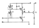
- the electronic switch consists of two MOSFETs 1 and 6, whose drain-source paths are connected in series. If the electronic switch is to switch a positive voltage + U, the first MOSFET 1 is an n-channel FET. The second MOSFET 6 is then a p-channel FET. If a negative voltage is to be switched, the FET 1 is a p-channel and the FET 6 is an n-channel FET. The FET 1 and 6 are connected on the drain side, the connection point 10 is connected to the output terminal A. The gate connection of the FET 1 is connected to the first input terminal E. It is also connected to the source connection of a deposition FET 7, the gate electrode of which is connected to the second input terminal M or ground.
- the drain connection of the FET 7 is connected via a resistor 8 to the supply voltage + U.
- the resistor 8 can, as shown in dashed lines, also be a further depletion FET, the gate connection of which is short-circuited to the source connection. This transistor then acts like a current squeeze with an infinitely high internal resistance.
- Depletion FET 7 and 8 have n-type channels. If a negative voltage is to be switched, depletion FET with p-channel should be used.
- FET 1 If a signal with the level H of z. B. +5 V, FET 1 is turned on and output A is at ground potential.
- the FET 7 receives a negative gate bias and is blocked. This means that there is high potential at the drain connection of the FET 7 and at the gate connection of the FET 6, as a result of which the FET 6 is blocked. The electronic switch is thus blocked, neither load current flows to the consumer 5 nor a cross current through the resistor 8 and the FET 7.
- the FET 1 If a signal with the level L of z. B. 0 V, the FET 1 is blocked and the depletion FET 7 receives the gate-source voltage 0 V. It is then switched on and a current can flow through the resistor 8 and the FET 7. A potential is then established at the gate connection of the p-channel FET 6, which is determined by the voltage divider ratio between resistor 8 and FET 7. This tension is positive and remains constant. The source connection of the FET 6 is at a constant voltage. The electronic switch can thus switch on very quickly and a capacitive load on the output terminal A, e.g. B. the gate capacitance of a power FET is charged very quickly.
- the gate-source path of the MOSFET 6 can with respect to voltage in the usual manner, for. B. protected by a Zener diode 9.
Description
Die Erfindung bezieht sich auf einen elektronischen Schalter mit den Merkmalen:
- a) Die Drain-Source-Strecke eines ersten und eines zweiten MOSFET sind zwischen einem ersten und einem zweiten Versorgungsspannungspotential in Reihe geschaltet,
- b) der erste und der zweite MOSFET sind Enhancement-FET und haben einander komplementäre Kanaltypen,
- c) der erste und zweite MOSFET sind drainseitig miteinander verbunden,
- d) der Verbindungspunkt beider MOSFET ist mit einer Ausgangsklemme verbunden,
- e) Die Drain-Source-Strecke eines dritten MOSFET, der vom gleichen Kanaltyp wie der erste MOSFET ist, ist über einen Widerstand mit dem zweiten Versorgungsspannungspotential verbunden,
- f) der Verbindungspunkt zwischen Widerstand und drittem MOSFET ist mit dem Gateanschluß des zweiten MOSFET verbunden,
- g) der Gateanschluß des ersten MOSFET ist mit einer ersten von zwei Steuereingangsklemmen verbunden,
- h) der Sourceanschluß des dritten MOSFET ist mit der ersten Eingangsklemme verbunden.
- a) the drain-source path of a first and a second MOSFET are connected in series between a first and a second supply voltage potential,
- b) the first and the second MOSFET are enhancement FET and have complementary channel types,
- c) the first and second MOSFETs are connected to one another on the drain side,
- d) the connection point of both MOSFETs is connected to an output terminal,
- e) the drain-source path of a third MOSFET, which is of the same channel type as the first MOSFET, is connected to the second supply voltage potential via a resistor,
- f) the connection point between the resistor and the third MOSFET is connected to the gate connection of the second MOSFET,
- g) the gate connection of the first MOSFET is connected to a first of two control input terminals,
- h) the source terminal of the third MOSFET is connected to the first input terminal.
Ein elektronischer Schalter dieser Art ist bereits im US-Patent 4 064 405 beschrieben worden. Der erwähnte dritte MOSFET ist ein Enhancement-FET, der bei Anlegen einer Eingangsspannung leitend gesteuert wird. Es fließt damit ein Strom durch den dem Enhancement-FET in Reihe geschalteten Widerstand und eine Diode, die zwischen dem Gateanschluß und dem Sourceanschluß des zweiten MOSFET angeschlossen ist. In diesem Zustand muß daher die Steuerspannungsquelle einen Strom liefern.An electronic switch of this type has already been described in U.S. Patent 4,064,405. The third MOSFET mentioned is an enhancement FET, which is turned on when an input voltage is applied. A current thus flows through the resistor connected in series with the enhancement FET and a diode which is connected between the gate connection and the source connection of the second MOSFET. In this state, the control voltage source must therefore supply a current.
Der Erfindung liegt die Aufgabe zugrunde, den elektronischen Schalter der bekannten Art so weiterzubilden, daß beim Anlegen einer Eingangsspannung kein wesentlicher Stromfluß auftritt.The invention has for its object to develop the electronic switch of the known type so that no significant current flow occurs when an input voltage is applied.
Diese Aufgabe wird gelöst durch die folgenden Merkmale:
- i) der dritte MOSFET ist ein Depletion-FET,
- k) der Gateanschluß des dritten MOSFET ist mit dem Sourceanschluß des ersten MOSFET und mit der zweiten Eingangsklemme verbunden.
- i) the third MOSFET is a depletion FET,
- k) the gate connection of the third MOSFET is connected to the source connection of the first MOSFET and to the second input terminal.
Die Erfindung wird anhand eines Ausführungsbeispiels in Verbindung mit der Figur näher erläutert. Weiterbildungen der Erfindung sind Gegenstand der Unteransprüche.The invention is explained in more detail using an exemplary embodiment in conjunction with the figure. Developments of the invention are the subject of the dependent claims.
Der elektronische Schalter nach besteht aus zwei MOSFET 1 und 6, deren Drain-Source-Strecken in Reihe geschaltet sind. Soll der elektronische Schalter eine positive Spannung +U schalten, so ist der erste MOSFET 1 ein n-Kanal-FET. Der zweite MOSFET 6 ist dann ein p-Kanal-FET. Soll eine negative Spannung geschaltet werden, so ist der FET 1 ein p-Kanal-und der FET 6 n-Kanal-FET. Die FET 1 und 6 sind drainseitig zusammengeschaltet, der Verbindungspunkt 10 ist mit der Ausgangsklemme A verbunden. Der Gateanschluß des FET 1 liegt an der ersten Eingangsklemme E. Er ist außerdem mit dem Sourceanschluß eines Depietion-FET 7 verbunden, dessen Gateelektrode an der zweiten Eingangsklemme M bzw. Masse liegt. Der Drainanschluß des FET 7 liegt über einem Widerstand 8 an der Versorgungsspannung +U. Der Widerstand 8 kann, wie gestrichelt dargestellt, auch ein weiterer Depletion-FET sein, dessen Gateanschluß mit dem Sourceanschluß kurzgeschlossen ist. Dieser Transistor wirkt dann wie eine Stromquetle mit unendlich hohem Innenwiderstand.The electronic switch according to consists of two MOSFETs 1 and 6, whose drain-source paths are connected in series. If the electronic switch is to switch a positive voltage + U, the first MOSFET 1 is an n-channel FET. The second MOSFET 6 is then a p-channel FET. If a negative voltage is to be switched, the FET 1 is a p-channel and the FET 6 is an n-channel FET. The FET 1 and 6 are connected on the drain side, the
Die Depletion-FET 7 und 8 haben n-leitende Kanäle. Soll eine negative Spannung geschaltet werden, so sind Depletion-FET mit p-Kanal zu verwenden.Depletion FET 7 and 8 have n-type channels. If a negative voltage is to be switched, depletion FET with p-channel should be used.
Wird an die Eingangsklemme E, M ein Signal mit dem Pegel H von z. B. +5 V gelegt, so wird der FET 1 aufgesteuert und der Ausgang A liegt auf Massepotential. Der FET 7 erhält eine negative Gatevorspannung und wird gesperrt. Damit liegt am Drainanschluß des FET 7 und am Gateanschluß des FET 6 hohes Potential an, wodurch der FET 6 gesperrt wird. Der elektronische Schalter ist damit gesperrt, es fließt weder Laststrom zum Verbraucher 5 noch ein Querstrom durch den Widerstand 8 und den FET 7.If a signal with the level H of z. B. +5 V, FET 1 is turned on and output A is at ground potential. The FET 7 receives a negative gate bias and is blocked. This means that there is high potential at the drain connection of the FET 7 and at the gate connection of the FET 6, as a result of which the FET 6 is blocked. The electronic switch is thus blocked, neither load current flows to the consumer 5 nor a cross current through the resistor 8 and the FET 7.
Wird an den Eingang E, M ein Signal mit dem Pegel L von z. B. 0 V gelegt, so wird der FET 1 gesperrt und der Depletion-FET 7 erhält die Gate-Source-Spannung 0 V. Er wird dann eingeschaltet und es kann ein Strom durch den Widerstand 8 und den FET 7 fließen. Am Gateanschluß des p-Kanal-FET 6 stellt sich dann ein Potential ein, das durch das Spannungsteilerverhältnis zwischen Widerstand 8 und FET 7 bestimmt ist. Diese Spannung ist positiv und bleibt konstant. Der Sourceanschluß des FET 6 liegt an einer konstanten Spannung. Der elektronische Schalter kann damit sehr schnell einschalten und eine an der Ausgangsklemme A liegende kapazitive Last, z. B. die Gate-Kapazität eines Leistungs-FET, wird sehr schnell aufgeladen.If a signal with the level L of z. B. 0 V, the FET 1 is blocked and the depletion FET 7 receives the gate-source voltage 0 V. It is then switched on and a current can flow through the resistor 8 and the FET 7. A potential is then established at the gate connection of the p-channel FET 6, which is determined by the voltage divider ratio between resistor 8 and FET 7. This tension is positive and remains constant. The source connection of the FET 6 is at a constant voltage. The electronic switch can thus switch on very quickly and a capacitive load on the output terminal A, e.g. B. the gate capacitance of a power FET is charged very quickly.
Die Gate-Source-Strecke des MOSFET 6 kann gegenüber Spannung auf übliche Weise, z. B. durch eine Zenerdiode 9, geschützt werden.The gate-source path of the MOSFET 6 can with respect to voltage in the usual manner, for. B. protected by a Zener diode 9.
Claims (1)
Applications Claiming Priority (2)
| Application Number | Priority Date | Filing Date | Title |
|---|---|---|---|
| DE3521090 | 1985-06-12 | ||
| DE3521090 | 1985-06-12 |
Publications (2)
| Publication Number | Publication Date |
|---|---|
| EP0205158A1 EP0205158A1 (en) | 1986-12-17 |
| EP0205158B1 true EP0205158B1 (en) | 1990-01-24 |
Family
ID=6273095
Family Applications (1)
| Application Number | Title | Priority Date | Filing Date |
|---|---|---|---|
| EP86107922A Expired - Lifetime EP0205158B1 (en) | 1985-06-12 | 1986-06-10 | Electronic switch |
Country Status (4)
| Country | Link |
|---|---|
| US (1) | US4677325A (en) |
| EP (1) | EP0205158B1 (en) |
| JP (1) | JPH0758899B2 (en) |
| DE (1) | DE3668522D1 (en) |
Families Citing this family (8)
| Publication number | Priority date | Publication date | Assignee | Title |
|---|---|---|---|---|
| JPH0760997B2 (en) * | 1986-06-09 | 1995-06-28 | 日本テキサス・インスツルメンツ株式会社 | High voltage output circuit |
| DE59207678D1 (en) * | 1992-06-05 | 1997-01-23 | Siemens Ag | Drive circuit for a power FET with source-side load |
| US5401973A (en) * | 1992-12-04 | 1995-03-28 | Atomic Energy Of Canada Limited | Industrial material processing electron linear accelerator |
| US5467050A (en) * | 1994-01-04 | 1995-11-14 | Texas Instruments Incorporated | Dynamic biasing circuit for semiconductor device |
| US5537072A (en) * | 1994-06-30 | 1996-07-16 | Sgs-Thomson Microelectronics, Inc. | Charge pump switch circuits |
| JP3228093B2 (en) * | 1995-06-28 | 2001-11-12 | 富士電機株式会社 | High voltage IC |
| GB2335556B (en) | 1998-03-18 | 2002-10-30 | Ericsson Telefon Ab L M | Switch circuit |
| US7400171B1 (en) * | 2005-05-03 | 2008-07-15 | Lattice Semiconductor Corporation | Electronic switch having extended voltage range |
Family Cites Families (6)
| Publication number | Priority date | Publication date | Assignee | Title |
|---|---|---|---|---|
| US952012A (en) * | 1908-11-05 | 1910-03-15 | Frederick Mayer | Wheel. |
| US3823330A (en) * | 1973-01-18 | 1974-07-09 | Inselek Inc | Circuit for shifting and amplifying input voltages |
| US4064405A (en) * | 1976-11-09 | 1977-12-20 | Westinghouse Electric Corporation | Complementary MOS logic circuit |
| NL7805068A (en) * | 1978-05-11 | 1979-11-13 | Philips Nv | THRESHOLD SWITCH. |
| JPS55136726A (en) * | 1979-04-11 | 1980-10-24 | Nec Corp | High voltage mos inverter and its drive method |
| JPS6079822A (en) * | 1983-10-07 | 1985-05-07 | Hitachi Ltd | Cmos integrated circuit device |
-
1986
- 1986-06-09 JP JP61133589A patent/JPH0758899B2/en not_active Expired - Fee Related
- 1986-06-09 US US06/872,354 patent/US4677325A/en not_active Expired - Lifetime
- 1986-06-10 DE DE8686107922T patent/DE3668522D1/en not_active Expired - Fee Related
- 1986-06-10 EP EP86107922A patent/EP0205158B1/en not_active Expired - Lifetime
Also Published As
| Publication number | Publication date |
|---|---|
| JPS61285820A (en) | 1986-12-16 |
| US4677325A (en) | 1987-06-30 |
| JPH0758899B2 (en) | 1995-06-21 |
| DE3668522D1 (en) | 1990-03-01 |
| EP0205158A1 (en) | 1986-12-17 |
Similar Documents
| Publication | Publication Date | Title |
|---|---|---|
| EP0747713B1 (en) | Circuit for measuring the load current of a power semiconductor device with a load on the source or drain side | |
| DE2411839C3 (en) | Integrated field effect transistor circuit | |
| DE2659207B2 (en) | Delay stage formed in a MOSFET integrated circuit | |
| DE3327260A1 (en) | SCHMITT TRIGGER | |
| EP0352659B1 (en) | Circuit for determining shorts in a load in series with a FET | |
| EP0304951B1 (en) | Optical coupler | |
| DE19638087C2 (en) | CMOS comparator | |
| DE2625007B2 (en) | Address buffer circuit for semiconductor memories | |
| EP0557850A2 (en) | Circuit arrangement for limiting the load current of a power MOSFET | |
| DE2356974A1 (en) | CONTACT DRIVER CIRCUIT CONSTRUCTED FROM FIELD EFFECT TRANSISTORS FOR DIGITAL APPLICATIONS | |
| EP0205158B1 (en) | Electronic switch | |
| EP0794619A2 (en) | Circuit for controlling a field-effect transistor having a load connected to its source | |
| EP0582125B1 (en) | Control circuit for a power MOSFET having a load connected to the source | |
| DE4444623A1 (en) | Power MOSFET load current control circuit | |
| DE2421988C2 (en) | Analog voltage switch | |
| DE2556683B2 (en) | Negative resistance network | |
| DE2061943C3 (en) | Differential amplifier | |
| DE2301855C3 (en) | Circuit arrangement with field effect transistors for level adjustment | |
| DE4403201C2 (en) | Drive circuit for a MOS semiconductor component with source-side load | |
| EP0405407A2 (en) | Circuit arrangement for controlling a MOSFET with a load connected to its source | |
| EP0365706B1 (en) | Power output stage with a load | |
| EP0753754A2 (en) | Integrated comparator circuit | |
| EP0544143B1 (en) | Integrated comparator circuit | |
| EP0825716A2 (en) | Drive circuit for a field-effect controlled semiconductor device | |
| DE3124891C2 (en) | Transistor switching stage |
Legal Events
| Date | Code | Title | Description |
|---|---|---|---|
| PUAI | Public reference made under article 153(3) epc to a published international application that has entered the european phase |
Free format text: ORIGINAL CODE: 0009012 |
|
| AK | Designated contracting states |
Kind code of ref document: A1 Designated state(s): DE FR GB IT |
|
| 17P | Request for examination filed |
Effective date: 19870127 |
|
| 17Q | First examination report despatched |
Effective date: 19881129 |
|
| GRAA | (expected) grant |
Free format text: ORIGINAL CODE: 0009210 |
|
| AK | Designated contracting states |
Kind code of ref document: B1 Designated state(s): DE FR GB IT |
|
| REF | Corresponds to: |
Ref document number: 3668522 Country of ref document: DE Date of ref document: 19900301 |
|
| ET | Fr: translation filed | ||
| ITF | It: translation for a ep patent filed |
Owner name: STUDIO JAUMANN |
|
| GBT | Gb: translation of ep patent filed (gb section 77(6)(a)/1977) | ||
| PLBE | No opposition filed within time limit |
Free format text: ORIGINAL CODE: 0009261 |
|
| STAA | Information on the status of an ep patent application or granted ep patent |
Free format text: STATUS: NO OPPOSITION FILED WITHIN TIME LIMIT |
|
| 26N | No opposition filed | ||
| ITTA | It: last paid annual fee | ||
| PGFP | Annual fee paid to national office [announced via postgrant information from national office to epo] |
Ref country code: DE Payment date: 20010823 Year of fee payment: 16 |
|
| REG | Reference to a national code |
Ref country code: GB Ref legal event code: IF02 |
|
| PGFP | Annual fee paid to national office [announced via postgrant information from national office to epo] |
Ref country code: GB Payment date: 20020610 Year of fee payment: 17 |
|
| PGFP | Annual fee paid to national office [announced via postgrant information from national office to epo] |
Ref country code: FR Payment date: 20020625 Year of fee payment: 17 |
|
| PG25 | Lapsed in a contracting state [announced via postgrant information from national office to epo] |
Ref country code: DE Free format text: LAPSE BECAUSE OF NON-PAYMENT OF DUE FEES Effective date: 20030101 |
|
| PG25 | Lapsed in a contracting state [announced via postgrant information from national office to epo] |
Ref country code: GB Free format text: LAPSE BECAUSE OF NON-PAYMENT OF DUE FEES Effective date: 20030610 |
|
| GBPC | Gb: european patent ceased through non-payment of renewal fee |
Effective date: 20030610 |
|
| PG25 | Lapsed in a contracting state [announced via postgrant information from national office to epo] |
Ref country code: FR Free format text: LAPSE BECAUSE OF NON-PAYMENT OF DUE FEES Effective date: 20040227 |
|
| REG | Reference to a national code |
Ref country code: FR Ref legal event code: ST |
|
| PG25 | Lapsed in a contracting state [announced via postgrant information from national office to epo] |
Ref country code: IT Free format text: LAPSE BECAUSE OF NON-PAYMENT OF DUE FEES;WARNING: LAPSES OF ITALIAN PATENTS WITH EFFECTIVE DATE BEFORE 2007 MAY HAVE OCCURRED AT ANY TIME BEFORE 2007. THE CORRECT EFFECTIVE DATE MAY BE DIFFERENT FROM THE ONE RECORDED. Effective date: 20050610 |