JP2018031705A - Semiconductor device - Google Patents
Semiconductor device Download PDFInfo
- Publication number
- JP2018031705A JP2018031705A JP2016164999A JP2016164999A JP2018031705A JP 2018031705 A JP2018031705 A JP 2018031705A JP 2016164999 A JP2016164999 A JP 2016164999A JP 2016164999 A JP2016164999 A JP 2016164999A JP 2018031705 A JP2018031705 A JP 2018031705A
- Authority
- JP
- Japan
- Prior art keywords
- terminal
- operational amplifier
- sense
- inverting input
- output
- Prior art date
- Legal status (The legal status is an assumption and is not a legal conclusion. Google has not performed a legal analysis and makes no representation as to the accuracy of the status listed.)
- Pending
Links
Images


Classifications
-
- G—PHYSICS
- G01—MEASURING; TESTING
- G01R—MEASURING ELECTRIC VARIABLES; MEASURING MAGNETIC VARIABLES
- G01R31/00—Arrangements for testing electric properties; Arrangements for locating electric faults; Arrangements for electrical testing characterised by what is being tested not provided for elsewhere
- G01R31/26—Testing of individual semiconductor devices
- G01R31/2607—Circuits therefor
- G01R31/2621—Circuits therefor for testing field effect transistors, i.e. FET's
-
- G—PHYSICS
- G01—MEASURING; TESTING
- G01R—MEASURING ELECTRIC VARIABLES; MEASURING MAGNETIC VARIABLES
- G01R19/00—Arrangements for measuring currents or voltages or for indicating presence or sign thereof
- G01R19/0092—Arrangements for measuring currents or voltages or for indicating presence or sign thereof measuring current only
-
- G—PHYSICS
- G01—MEASURING; TESTING
- G01R—MEASURING ELECTRIC VARIABLES; MEASURING MAGNETIC VARIABLES
- G01R31/00—Arrangements for testing electric properties; Arrangements for locating electric faults; Arrangements for electrical testing characterised by what is being tested not provided for elsewhere
- G01R31/40—Testing power supplies
- G01R31/42—AC power supplies
-
- H—ELECTRICITY
- H03—ELECTRONIC CIRCUITRY
- H03K—PULSE TECHNIQUE
- H03K2217/00—Indexing scheme related to electronic switching or gating, i.e. not by contact-making or -breaking covered by H03K17/00
- H03K2217/0027—Measuring means of, e.g. currents through or voltages across the switch
Abstract
Description
本発明は、力行時と回生時における双方向の電流を検出する半導体装置に関する。 The present invention relates to a semiconductor device that detects bidirectional current during power running and regeneration.
従来から、IGBTやMOSFETなどのパワースイッチング素子を流れる電流を検出する手段として、シャント抵抗器や電流センサを利用するものが知られている。しかしながら、シャント抵抗器は、抵抗器自身に流れる電流による損失が生じてしまい省エネルギー化の要請に反する。また、電流センサは、シャント抵抗器よりも高コストになる場合がある。 Conventionally, as a means for detecting a current flowing through a power switching element such as an IGBT or a MOSFET, one using a shunt resistor or a current sensor is known. However, the shunt resistor causes a loss due to the current flowing through the resistor itself, which is against the demand for energy saving. Also, current sensors may be more expensive than shunt resistors.
このような問題に対し、特許文献1に開示された発明は、MOSFETのソース電圧をオペアンプに入力して出力をフィードバックする構成を採用することにより、シャント抵抗器や電流センサを用いることなく、高精度にスイッチング素子の電流を検出することができる。 In order to solve such a problem, the invention disclosed in Patent Document 1 adopts a configuration in which the source voltage of the MOSFET is input to the operational amplifier and the output is fed back, so that a high voltage can be obtained without using a shunt resistor or a current sensor. The current of the switching element can be detected with high accuracy.
しかしながら、特許文献1に開示された発明では、ドレインからソースに流れる電流(例えば力行時)の電流値を検出することはできるものの、ソースからドレインに流れる電流(例えば回生時)の電流値を検出することはできない。 However, although the invention disclosed in Patent Document 1 can detect the current value of the current flowing from the drain to the source (for example, during power running), the current value of the current flowing from the source to the drain (for example during regeneration) is detected. I can't do it.
回生時の電流を検出する技術には、シャント抵抗器を利用するものが知られているが、電力損失の観点から好ましくない。 As a technique for detecting a current during regeneration, one using a shunt resistor is known, but it is not preferable from the viewpoint of power loss.
そこで、本発明は上記問題点に鑑み、電力損失を抑えつつ、高精度且つ、力行時と回生時の双方向の電流検出が可能な半導体装置を提供することを目的とする。 In view of the above problems, an object of the present invention is to provide a semiconductor device capable of highly accurate and bidirectional current detection during powering and regeneration while suppressing power loss.
ここに開示される発明は、上記目的を達成するために以下の技術的手段を採用する。なお、特許請求の範囲およびこの項に記載した括弧内の符号は、ひとつの態様として後述する実施形態に記載の具体的手段との対応関係を示すものであって、発明の技術的範囲を限定するものではない。 The invention disclosed herein employs the following technical means to achieve the above object. Note that the reference numerals in parentheses described in the claims and in this section indicate a corresponding relationship with specific means described in the embodiments described later as one aspect, and limit the technical scope of the invention. Not what you want.
上記目的を達成するために、本発明は、負荷電流を制御するメインスイッチング素子(Mtr)と、メインスイッチング素子にカレントミラー接続されて負荷電流に相関するセンス電流が流れるセンススイッチング素子(Str)と、を備え、
メインスイッチング素子は、出力端子として互いの間を電流が流れる第1端子(T1)および第2端子(T2)を有し、センススイッチング素子は、第1端子に接続される第3端子(T3)と、第3端子との間で前記センス電流が流れる第4端子(T4)と、を有し、
第4端子に接続され、第4端子の電位を検出するためのセンス抵抗(23)を備えた半導体装置であって、
さらに、前記第2端子および前記第4端子がそれぞれ入力端子に接続されるオペアンプ(OP1,OP2,OP3,OP4)を備え、
オペアンプは、オペアンプの出力がオペアンプの入力端子にフィードバックするように構成されつつ、そのフィードバック経路にセンス抵抗を含むようにされ、
さらに、オペアンプには、第1端子よりも高い電圧(VH)が供給可能にされており、
第1端子と、第2端子または第4端子と、の大小関係に応じてセンス抵抗に流れるセンス電流の方向が切り替え可能にされる。
In order to achieve the above object, the present invention includes a main switching element (Mtr) that controls a load current, a sense switching element (Str) that is connected to the main switching element as a current mirror and through which a sense current correlated with the load current flows. With
The main switching element has a first terminal (T1) and a second terminal (T2) through which current flows as an output terminal, and the sense switching element is a third terminal (T3) connected to the first terminal. And a fourth terminal (T4) through which the sense current flows between the third terminal and
A semiconductor device including a sense resistor (23) connected to the fourth terminal for detecting the potential of the fourth terminal,
The second terminal and the fourth terminal further include operational amplifiers (OP1, OP2, OP3, OP4) connected to input terminals, respectively.
The operational amplifier is configured so that the output of the operational amplifier feeds back to the input terminal of the operational amplifier, and the feedback path includes a sense resistor.
Furthermore, the operational amplifier can be supplied with a higher voltage (VH) than the first terminal,
The direction of the sense current flowing through the sense resistor can be switched according to the magnitude relationship between the first terminal and the second terminal or the fourth terminal.
これによれば、センス抵抗がオペアンプの出力と入力との間のフィードバック経路内に構成されているから、フィードバック電流の方向によってセンス抵抗を流れる電流の向きを切り替えることができる。すなわち、センス電流の方向を切り替えることができる。そして、この構成では、例えば第1端子よりも第4端子の電位が低いとき(力行時)に流れるセンス電流の方向と、第1端子よりも第4端子の電位が高いとき(回生時)に流れるセンス電流の方向とを互いに逆向きにすることができる。このため、力行時に加えて回生時においてもセンス電流の電流値を検出でき、ひいてはメインスイッチング素子の出力電流を検出することができる。なお、第1端子よりも第4端子の電位が高い回生時であっても、オペアンプには第1端子よりも高い電圧が供給可能にされているから、センス電流を第4端子が接続された入力端子に向かって流すことができる。すなわち、回生時において力行時とは逆向きのセンス電流を流すことができる。 According to this, since the sense resistor is configured in the feedback path between the output and the input of the operational amplifier, the direction of the current flowing through the sense resistor can be switched depending on the direction of the feedback current. That is, the direction of the sense current can be switched. In this configuration, for example, the direction of the sense current flowing when the potential of the fourth terminal is lower than that of the first terminal (during powering) and when the potential of the fourth terminal is higher than that of the first terminal (during regeneration). The direction of the flowing sense current can be opposite to each other. For this reason, the current value of the sense current can be detected not only during power running but also during regeneration, and as a result, the output current of the main switching element can be detected. Even when the potential of the fourth terminal is higher than that of the first terminal, since the operational amplifier can supply a voltage higher than that of the first terminal, the sense current is connected to the fourth terminal. It can flow toward the input terminal. That is, it is possible to flow a sense current in a direction opposite to that during power running during regeneration.
また、この構成では、オペアンプの負帰還動作によるフィードバック電流をセンス電流として利用するから、メインスイッチング素子とセンススイッチング素子との間で出力端子間の電位差を略同一に維持することができる。このため、メインスイッチング素子とセンススイッチング素子とのミラー比ずれを抑制できるので、センススイッチング素子を流れるセンス電流と、メインスイッチング素子を流れる出力電流との相関を高精度にとることができる。すなわち、メインスイッチング素子を流れる出力電流の検出を、安価且つ高精度に行うことができる。 Further, in this configuration, since the feedback current due to the negative feedback operation of the operational amplifier is used as the sense current, the potential difference between the output terminals can be maintained substantially the same between the main switching element and the sense switching element. For this reason, since a mirror ratio shift between the main switching element and the sense switching element can be suppressed, the correlation between the sense current flowing through the sense switching element and the output current flowing through the main switching element can be obtained with high accuracy. That is, the output current flowing through the main switching element can be detected at low cost and with high accuracy.
以下、本発明の実施の形態を図面に基づいて説明する。なお、以下の各図相互において、互いに同一もしくは均等である部分に、同一符号を付与する。 Hereinafter, embodiments of the present invention will be described with reference to the drawings. In the following drawings, the same reference numerals are given to the same or equivalent parts.
(第1実施形態)
最初に、図1を参照して、本実施形態に係る半導体装置の概略構成について説明する。
(First embodiment)
First, a schematic configuration of the semiconductor device according to the present embodiment will be described with reference to FIG.
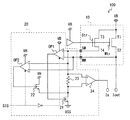
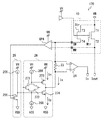
図1に示すように、この半導体装置100は、パワースイッチング素子10と、パワースイッチング素子に流れる出力電流を検出する電流検出部20を備えたスイッチ装置である。本実施形態において、所定の電圧源から端子に与えられる電位には、電源電位VBと、電源電位VBよりも高電位に昇圧された昇圧電位VHと、回路の基準電位VSSとがある。各電位の大小関係はVH>VB>VSSである。VSSは例えばグランド電位であり、VBは例えば車両におけるバッテリ電位であり、VHはバッテリ電位をチャージポンプ等で昇圧した電位である。
As shown in FIG. 1, the
パワースイッチング素子10は、図示しない負荷に出力電流Ioutを供給するメインスイッチング素子たるメインMOSトランジスタMtrと、メインMOSトランジスタMtrとの間で互いのドレインが接続されてカレントミラー接続されたセンスMOSトランジスタStrとを有している。
The
メインMOSトランジスタMtrは、例えばNchMOSトランジスタである。第1端子たるドレイン端子T1には電源が接続され電源電位VBとされている。一方、第2端子たるソース端子T2は、メインMOSトランジスタMtrを流れる電流である出力電流Ioutを取り出す端子である。つまり、ソース端子T2に負荷が接続される。ドレイン端子T1よりもソース端子T2が低電位のとき、すなわち力行時において、ゲート端子にゲート電圧が印加されると、出力電流Ioutはドレイン端子T1からソース端子T2に向かって流れる。逆に、ドレイン端子T1よりもソース端子T2が高電位のとき、すなわち回生時においても、ゲート電圧を印加してメインMOSトランジスタMtrをオンさせる同期整流を行う。これにより、出力電流Ioutは、メインMOSトランジスタMtrとセンスMOSトランジスタStrのミラー比に基づいて、ソース端子T2からドレイン端子T1に向かって流れる。なお、図1に示すように、第2端子たるソース端子T2の電位をMMと示し、この電位は後述の第1オペアンプOP1における反転入力端子、および第2オペアンプOP2における非反転入力端子に印加される。 The main MOS transistor Mtr is, for example, an Nch MOS transistor. A power supply is connected to the drain terminal T1, which is the first terminal, and is set to the power supply potential VB. On the other hand, the source terminal T2 as the second terminal is a terminal for taking out an output current Iout which is a current flowing through the main MOS transistor Mtr. That is, a load is connected to the source terminal T2. When the gate voltage is applied to the gate terminal when the source terminal T2 is at a lower potential than the drain terminal T1, that is, during powering, the output current Iout flows from the drain terminal T1 toward the source terminal T2. Conversely, even when the source terminal T2 has a higher potential than the drain terminal T1, that is, during regeneration, synchronous rectification is performed to turn on the main MOS transistor Mtr by applying a gate voltage. Thus, the output current Iout flows from the source terminal T2 toward the drain terminal T1 based on the mirror ratio of the main MOS transistor Mtr and the sense MOS transistor Str. As shown in FIG. 1, the potential of the source terminal T2, which is the second terminal, is denoted as MM, and this potential is applied to the inverting input terminal of the first operational amplifier OP1 described later and the non-inverting input terminal of the second operational amplifier OP2. The
センスMOSトランジスタStrは、例えばNchMOSトランジスタである。センスMOSトランジスタStrはメインMOSトランジスタMtrにカレントミラー接続されている。すなわち、第3端子たるドレイン端子T3はメインMOSトランジスタMtrのドレイン端子T1に接続されて電源電位VBとされている。そして、メインMOSトランジスタMtrと同一のゲート電圧がゲート端子に印加される。センスMOSトランジスタStrのドレイン端子T3と第4端子たるソース端子T4の間にはセンス電流Isが流れる。センス電流Isは、メインMOSトランジスタMtrとの間で規定されるミラー比に応じた大きさを持ち、電流の向きは出力電流Ioutと同方向である。つまり、ドレイン端子T3よりもソース端子T4が低電位のとき、すなわち力行時において、ゲート端子にゲート電圧が印加されると、センス電流Isはドレイン端子T3からソース端子T4に向かって流れる。逆に、ドレイン端子T3よりもソース端子T4が高電位のとき、すなわち回生時においても、ゲート電圧を印加してセンスMOSトランジスタStrをオンさせる同期整流を行う。これにより、センス電流Isは、ソース端子T4からドレイン端子T3に向かって流れる。なお、図1に示すように、第4端子たるソース端子T4の電位をSMと示し、この電位は後述の第1オペアンプOP1における非反転入力端子、および第2オペアンプOP2における反転入力端子に印加される。 The sense MOS transistor Str is, for example, an Nch MOS transistor. The sense MOS transistor Str is connected to the main MOS transistor Mtr as a current mirror. That is, the drain terminal T3 as the third terminal is connected to the drain terminal T1 of the main MOS transistor Mtr and is set to the power supply potential VB. Then, the same gate voltage as that of the main MOS transistor Mtr is applied to the gate terminal. A sense current Is flows between the drain terminal T3 of the sense MOS transistor Str and the source terminal T4 as the fourth terminal. The sense current Is has a magnitude corresponding to the mirror ratio defined between the main MOS transistor Mtr and the direction of the current is the same direction as the output current Iout. That is, when the gate voltage is applied to the gate terminal when the source terminal T4 is at a lower potential than the drain terminal T3, that is, during powering, the sense current Is flows from the drain terminal T3 toward the source terminal T4. Conversely, even when the source terminal T4 is at a higher potential than the drain terminal T3, that is, during regeneration, synchronous rectification is performed to turn on the sense MOS transistor Str by applying a gate voltage. As a result, the sense current Is flows from the source terminal T4 toward the drain terminal T3. As shown in FIG. 1, the potential of the source terminal T4 as the fourth terminal is denoted by SM, and this potential is applied to the non-inverting input terminal of the first operational amplifier OP1 described later and the inverting input terminal of the second operational amplifier OP2. The
上記したように、センス電流Isは出力電流Ioutに相関する。よって、出力電流Ioutを直接測定せずとも、センス電流Isを検出できれば出力電流Ioutを知ることができる。なお、以降のセンス電流Isおよび出力電流Ioutの記載においては、ドレインからソースに向かって電流が流れる力行時の電流の向きを正とし、回生時の電流の向きを負とする。 As described above, the sense current Is correlates with the output current Iout. Therefore, the output current Iout can be known if the sense current Is can be detected without directly measuring the output current Iout. In the subsequent description of the sense current Is and the output current Iout, the direction of the current during power running in which the current flows from the drain to the source is positive, and the direction of the current during regeneration is negative.
電流検出部20は、以下に詳述するオペアンプOP1,OP2の負帰還動作によるフィードバック電流をセンス電流Isとして利用する。電流検出部20は、図1に示すように、第1オペアンプOP1と、第2オペアンプOP2と、第1トランジスタ21と、第2トランジスタ22と、センス抵抗23と、センス電流検出アンプ24と、を有している。
The
第1オペアンプOP1は、電源電位VBを電源として駆動する一般的なオペアンプである。第1オペアンプOP1の非反転入力端子にはセンスMOSトランジスタStrのソース端子T4が接続されている。第1オペアンプOP1の反転入力端子にはメインMOSトランジスタMtrのソース端子T2が接続されている。 The first operational amplifier OP1 is a general operational amplifier that is driven using the power supply potential VB as a power supply. The source terminal T4 of the sense MOS transistor Str is connected to the non-inverting input terminal of the first operational amplifier OP1. The source terminal T2 of the main MOS transistor Mtr is connected to the inverting input terminal of the first operational amplifier OP1.
第1オペアンプOP1の出力端子は、NMOSで構成された第1トランジスタ21のゲート端子に接続されている。第1トランジスタ21のソース端子は基準電位VSSに接続され、第1トランジスタ21のドレイン端子はセンス抵抗23を介して第1オペアンプOP1の非反転入力端子に接続されている。つまり、第1オペアンプOP1の出力端子は、第1トランジスタ21およびセンス抵抗23がこの順番で仲介して非反転入力端子に接続されている。なお、基準電位VSSは、例えばグランド電位GNDである。
The output terminal of the first operational amplifier OP1 is connected to the gate terminal of the
このように、第1オペアンプOP1は、出力端子がセンス抵抗23を介して非反転入力端子に負帰還で接続された構成とされている。そして、非反転入力端子と反転入力端子との間に電位差が生じた場合において、非反転入力端子から基準電位VSSに向かってフィードバック電流が流れることにより、非反転入力端子と反転入力端子との電位差が小さくなるように動作する。つまり、これはセンスMOSトランジスタStrのソース端子T4から基準電位VSSに向かって電流が流出することを意味し、このときのフィードバック電流がセンス電流Isとしてセンス抵抗23に流れる。このようなセンス電流Isの流れは、ソース端子T4の電位であるSMが電源電位VBよりも低電位となる力行時に発生する。
As described above, the first operational amplifier OP1 has a configuration in which the output terminal is connected to the non-inverting input terminal via the
第2オペアンプOP2は、昇圧電位VHを電源として駆動する一般的なオペアンプである。第2オペアンプOP2の反転入力端子にはセンスMOSトランジスタStrのソース端子T4が接続されている。第2オペアンプOP2の非反転入力端子にはメインMOSトランジスタMtrのソース端子T2が接続されている。 The second operational amplifier OP2 is a general operational amplifier that is driven using the boosted potential VH as a power source. The source terminal T4 of the sense MOS transistor Str is connected to the inverting input terminal of the second operational amplifier OP2. The non-inverting input terminal of the second operational amplifier OP2 is connected to the source terminal T2 of the main MOS transistor Mtr.
第2オペアンプOP2の出力端子は、NMOSで構成された第2トランジスタ22のゲート端子に接続されている。第2トランジスタ22のドレイン端子は昇圧電位VHに接続され、第2トランジスタ22のソース端子はセンス抵抗23を介して第2オペアンプOP2の反転入力端子に接続されている。つまり、第2オペアンプOP2の出力端子は、第2トランジスタ22およびセンス抵抗23がこの順番で仲介して反転入力端子に接続されている。
The output terminal of the second operational amplifier OP2 is connected to the gate terminal of the
このように、第2オペアンプOP2は、出力端子がセンス抵抗23を介して反転入力端子に負帰還で接続された構成とされている。そして、非反転入力端子と反転入力端子との間に電位差が生じた場合において、昇圧電位VHから反転入力端子に向かってフィードバック電流が流れることにより、非反転入力端子と反転入力端子との電位差が小さくなるように動作する。つまり、これは昇圧電位VHからセンスMOSトランジスタStrのソース端子T4に向かって電流が流出することを意味し、このときのフィードバック電流がセンス電流Isとしてセンス抵抗23に流れる。このようなセンス電流Isの流れは、ソース端子T4の電位であるSMが電源電位VBよりも高電位となる回生時に発生し、力行時におけるセンス電流の向きとは逆向きになる。本実施形態では、昇圧電位VHは電源電位VBよりも高電位であるから、SM>VBの回生時もセンス電流が流れる。
Thus, the second operational amplifier OP2 has a configuration in which the output terminal is connected to the inverting input terminal via the
なお、図1に示すように、第1オペアンプOP1および第2オペアンプOP2には、それぞれの動作をオンまたはオフするための信号SIGが入力されている。ここで、オペアンプをオンするとは、アンプとしての機能を発揮させて出力端子から信号を出力させることを意味する。また、オペアンプをオフするとは、出力端子からの信号出力を遮断することを意味する。信号SIGは、第1端子たるドレイン端子T1の電位と、第2端子たるソース端子T2の電位との大小関係がMM<VBのとき、あるいは、第1端子たるドレイン端子T1の電位と、第4端子たるソース端子T4の電位との大小関係がSM<VBのとき、第1オペアンプOP1をオンし、第2オペアンプOP2をオフする。一方、信号SIGは、MM>VB(あるいはSM>VB)のとき第1オペアンプOP1をオフし、第2オペアンプOP2をオンする。 As shown in FIG. 1, the first operational amplifier OP1 and the second operational amplifier OP2 are supplied with a signal SIG for turning on or off the respective operations. Here, turning on the operational amplifier means that a signal is output from the output terminal by exhibiting the function as an amplifier. Also, turning off the operational amplifier means shutting off the signal output from the output terminal. The signal SIG is generated when the magnitude relationship between the potential of the drain terminal T1 that is the first terminal and the potential of the source terminal T2 that is the second terminal is MM <VB, or the potential of the drain terminal T1 that is the first terminal, When the magnitude relationship with the potential of the source terminal T4 as a terminal is SM <VB, the first operational amplifier OP1 is turned on and the second operational amplifier OP2 is turned off. On the other hand, the signal SIG turns off the first operational amplifier OP1 and turns on the second operational amplifier OP2 when MM> VB (or SM> VB).
センス電流検出アンプ24は、一般的に知られたオペアンプである。センス抵抗23に対して第1オペアンプOP1の非反転入力端子側、あるいは第2オペアンプOP2の反転入力端子側の一端に、センス電流検出アンプ24の非反転入力端子が接続されている。一方、センス抵抗23の他端にセンス電流検出アンプ24の反転入力端子が接続されている。よって、センス電流検出アンプ24は、非反転入力端子の電位が反転入力端子よりも高い力行時には、センス電流値に相関した正の出力値を出力する。一方、センス電流検出アンプ24は、非反転入力端子の電位が反転入力端子よりも低い回生時には、センス電流値に相関した負の出力値を出力する。
The sense
次に、本実施形態における半導体装置100を採用することによる作用効果について説明する。
Next, functions and effects obtained by employing the
この半導体装置100は、SM<VBあるいはMM<VBとなる力行時において、第1オペアンプOP1がオンされて有効になり、第2オペアンプOP2がオフされて無効になる。第1オペアンプOP1はSMがMMに等しくなるように負帰還動作する。その過程で、第1トランジスタ21がオンされて第1オペアンプOP1の非反転入力端子からセンス抵抗23を経て基準電位VSSに向かってフィードバック電流が流れ、このフィードバック電流がセンス電流として検出される。このように、この半導体装置100は、メインMOSトランジスタMtrのドレイン−ソース間電圧と、センスMOSトランジスタStrのドレイン−ソース間電圧とを同値に維持した状態で力行時のセンス電流を検出することができる。よって、メインMOSトランジスタMtrとセンスMOSトランジスタStrとでアーリー効果による電位差ずれを生ずることなく、正しいミラー比を維持したまま力行時の出力電流Ioutを高精度に検出することができる。
In the
また、この半導体装置100は、SM>VBあるいはMM>VBとなる回生時において、第2オペアンプOP2がオンされて有効になり、第1オペアンプOP1がオフされて無効になる。第2オペアンプOP2はSMがMMに等しくなるように負帰還動作する。その過程で、第2トランジスタ22がオンされて昇圧電位VHからセンス抵抗23を経て第2オペアンプOP1の非反転入力端子に向かってフィードバック電流が流れ、このフィードバック電流がセンス電流として検出される。このように、この半導体装置100は、メインMOSトランジスタMtrのドレイン−ソース間電圧と、センスMOSトランジスタStrのドレイン−ソース間電圧とを同値に維持した状態で回生時のセンス電流を検出することができる。よって、同期整流時においては、メインMOSトランジスタMtrとセンスMOSトランジスタStrとでアーリー効果による電位差ずれを生ずることなく、正しいミラー比を維持したまま回生時の出力電流Ioutを高精度に検出することができる。
In addition, in the
上記のとおり、この半導体装置100は、高精度に出力電流Ioutに相関するセンス電流Isを、その向きを含めて検出することができる。加えて、この半導体装置100では、メインMOSトランジスタMtrの出力端子であるソース端子T2に、電流検出用のシャント抵抗器を設けないから、出力電流に対する電力損失は無い。
As described above, the
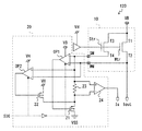
(変形例1)
上記した第1実施形態では、メインMOSトランジスタMtrのドレイン端子T1が電源電位VBとされ、負荷に対して、いわゆるハイサイド側のMOSトランジスタを想定した構成について説明したが、図2に示すように、負荷に対してローサイド側のMOSトランジスタに対しても同様の構成を採用することができる。
(Modification 1)
In the first embodiment described above, the drain terminal T1 of the main MOS transistor Mtr is set to the power supply potential VB, and a configuration assuming a so-called high-side MOS transistor with respect to the load has been described. As shown in FIG. The same configuration can be adopted for the MOS transistor on the low side with respect to the load.
この半導体装置110の、第1実施形態における半導体装置100と異なる点の一つは、メインMOSトランジスタMtrのソース端子T2がグランド電位GNDに接続され、ドレイン端子T1に負荷が接続される点である。また、二つは、第1トランジスタ21のソース端子の電位VSSがグランド電位GNDよりも低電位に設定され、第2トランジスタ22のドレイン端子が電源電位VBに接続される点である。
One of the differences of the
一つめの相違点は、メインMOSトランジスタMtrが負荷に対してローサイド側に接続されることに起因するものである。 The first difference is due to the fact that the main MOS transistor Mtr is connected to the low side with respect to the load.
二つめの相違点のうち、第1トランジスタ21のソース端子の電位VSSをグランド電位GNDより低電位に設定することは必須である。力行時において、第1オペアンプOP1は比反転入力端子の電位SMを、反転入力端子の電位MM(=GND)に等しくなるように基準電位VSSに向かってフィードバック電流を流す。この動作は、基準電位VSSをグランド電位GNDよりも低電位にすることで実現することができる。
Among the second differences, it is essential to set the potential VSS of the source terminal of the
なお、第2トランジスタ22のドレイン端子に接続する電位は、本変形例では電源電位VBとしているが、昇圧電位VHであっても構わない。
Note that the potential connected to the drain terminal of the
本変形例においても、第1実施形態と同様に、力行時においては第1オペアンプOP1がオンされ、回生時においては第2オペアンプOP2がオンされることにより、高精度に出力電流Ioutに相関するセンス電流Isを、その向きを含めて検出することができる。 Also in the present modification, as in the first embodiment, the first operational amplifier OP1 is turned on during power running, and the second operational amplifier OP2 is turned on during regeneration, so that it correlates with the output current Iout with high accuracy. The sense current Is can be detected including its direction.
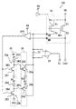
(変形例2)
上記した第1実施形態では、第1オペアンプOP1および第2オペアンプOP2を有効にした際にフィードバック経路を構成する第1トランジスタ21および第2トランジスタ22がNchのMOSトランジスタである例について説明した。
(Modification 2)
In the first embodiment described above, an example has been described in which the
ここで、第1トランジスタ21および第2トランジスタ22は、それぞれ第1オペアンプOP1および第2オペアンプOP2が有効にされたときにフィードバック経路を形成するように動作すれば良いのであって、NchのMOSトランジスタに限定されない。例えば、図3に示す半導体装置120における第1トランジスタ21および第2トランジスタ22は、PchのMOSトランジスタ(PMOS)である。
Here, the
半導体装置120では、第1オペアンプOP1の入力端子の構成も第1実施形態に対して逆転する。また、第2オペアンプOP2の入力端子の構成も第1実施形態に対して逆転する。具体例には、メインMOSトランジスタMtrのソース端子T2は、第1オペアンプOP1の非反転入力端子、および、第2オペアンプOP2の反転入力端子に接続される。また、センスMOSトランジスタStrのソース端子T4は、第1オペアンプOP1の反転入力端子、および、第2オペアンプOP2の非反転入力端子に接続される。
In the
このように構成することにより、力行時には、第1オペアンプOP1の属するフィードバック経路において、第1オペアンプOP1の反転入力端子から基準電位VSSに向かってセンス電流Isが流れる。また、回生時には、第2オペアンプOP2の属するフィードバック経路において、昇圧電位VHから第2オペアンプOP2の非反転入力端子に向かってセンス電流Isが流れる。 With this configuration, at the time of power running, a sense current Is flows from the inverting input terminal of the first operational amplifier OP1 toward the reference potential VSS in the feedback path to which the first operational amplifier OP1 belongs. During regeneration, a sense current Is flows from the boosted potential VH toward the non-inverting input terminal of the second operational amplifier OP2 in the feedback path to which the second operational amplifier OP2 belongs.
すなわち、第1実施形態と同様に、高精度に出力電流Ioutに相関するセンス電流Isを、その向きを含めて検出することができる。 That is, as in the first embodiment, the sense current Is correlated with the output current Iout can be detected with high accuracy including its direction.
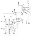
(第2実施形態)
第1実施形態およびその変形例1,2では、センス電流としてのフィードバック電流を生成するためのオペアンプを2つ備える形態について説明した。これに対して、本実施形態における半導体装置130は、唯一のオペアンプOP3によって第1実施形態と同様の効果を発揮する。
(Second Embodiment)
In the first embodiment and the first and second modifications thereof, the mode in which two operational amplifiers for generating a feedback current as a sense current are provided has been described. On the other hand, the
本実施形態における半導体装置130は、図4に示すように、第1実施形態と同一のパワースイッチング素子10に、唯一のオペアンプOP3が接続されている。オペアンプOP3には昇圧電位VHが電源として入力され、2つの入力端子は、第1スイッチ回路31を介してメインMOSトランジスタMtrおよびセンスMOSトランジスタStrのソース端子T2,T4に接続されている。また、オペアンプOP3の出力端子は、第2スイッチ回路32を介して、第1トランジスタ21および第2トランジスタ22に接続されている。
In the
具体的には、図4に示すように、第1スイッチ回路31は、2つのスイッチSW1と、2つのスイッチSW2とを有している。メインMOSトランジスタMtrの第2端子たるソース端子T2は、スイッチSW1を介してオペアンプOP3の反転入力端子に接続されつつ、スイッチSW2を介して非反転入力端子に接続されている。つまり、ソース端子T2は、スイッチSW1がオンのときは反転入力端子に接続され、スイッチSW2がオンのときは非反転入力端子に接続される。センスMOSトランジスタStrの第4端子たるソース端子T4は、スイッチSW1を介してオペアンプOP3の非反転入力端子に接続されつつ、スイッチSW2を介して反転入力端子に接続されている。つまり、ソース端子T4は、スイッチSW1がオンのときは非反転入力端子に接続され、スイッチSW2がオンのときは反転入力端子に接続される。なお、センス抵抗23は、第4端子T4と第1スイッチ回路31との中間点に接続されている。
Specifically, as shown in FIG. 4, the
第2スイッチ回路32は、1つのスイッチSW1と、1つのスイッチSW2を有している。オペアンプOP3の出力端子は、スイッチSW1を介して第1トランジスタ21のゲート端子に入力されている。一方、出力端子は、スイッチSW2を介して第2トランジスタ22のゲート端子にも接続されている。第1トランジスタ21のドレイン端子はセンス抵抗23を介してオペアンプOP3の非反転入力端子に接続され、第2トランジスタ22のソース端子はセンス抵抗23を介してオペアンプOP3の非反転入力端子に接続されている。
The
すなわち、オペアンプOP3は、スイッチSW1がオンすると第1トランジスタ21とセンス抵抗23を含むフィードバック経路を形成する負帰還回路を成し、スイッチSW2がオンすると第2トランジスタ22とセンス抵抗23を含むフィードバック経路を形成する負帰還回路を成す。換言すれば、スイッチSW1がオンすると、オペアンプOP3は、第1実施形態における第1オペアンプOP1と同様の機能を奏する。一方、スイッチSW2がオンすると、オペアンプOP3は、第1実施形態における第2オペアンプOP2と同様の機能を奏する。
That is, the operational amplifier OP3 forms a negative feedback circuit that forms a feedback path including the
なお、第1実施形態では、第1端子たるドレイン端子T1の電位と、第2端子たるソース端子T2の電位との大小関係に応じて各オペアンプOP1,OP2をオンオフする信号SIGがオペアンプOP1,OP2に入力される例を示した。これに対して、本実施形態における信号SIGは、第1スイッチ回路31および第2スイッチ回路32におけるスイッチSW1およびスイッチSW2のオンオフを制御する。スイッチSW1とスイッチSW2とは同期しており、スイッチSW1がオンのときスイッチSW2はオフする。また、スイッチSW2がオンのときスイッチSW1はオフする。
In the first embodiment, the signals SIG for turning on and off the operational amplifiers OP1 and OP2 according to the magnitude relationship between the potential of the drain terminal T1 as the first terminal and the potential of the source terminal T2 as the second terminal are the operational amplifiers OP1 and OP2. An example of input is shown. On the other hand, the signal SIG in the present embodiment controls on / off of the switch SW1 and the switch SW2 in the
信号SIGは、第1端子たるドレイン端子T1の電位と、第2端子たるソース端子T2の電位との大小関係がMM<VBのとき、あるいは、第1端子たるドレイン端子T1の電位と、第4端子たるソース端子T4の電位との大小関係がSM<VBのとき(力行時)、スイッチSW1をオンし、スイッチSW2をオフする。一方、信号SIGは、MM>VB(あるいはSM>VB)のとき(回生時)、スイッチSW1をオフし、スイッチSW2をオンする。 The signal SIG is generated when the magnitude relationship between the potential of the drain terminal T1 that is the first terminal and the potential of the source terminal T2 that is the second terminal is MM <VB, or the potential of the drain terminal T1 that is the first terminal, When the magnitude relationship with the potential of the source terminal T4 as a terminal is SM <VB (during powering), the switch SW1 is turned on and the switch SW2 is turned off. On the other hand, the signal SIG turns off the switch SW1 and turns on the switch SW2 when MM> VB (or SM> VB) (regeneration).
これにより、唯一のオペアンプOP3によって、力行時および回生時のいずれのセンス電流も検出することができる。また、回路規模の大きいオペアンプの点数を第1実施形態およびその変形例1,2に較べて減ずることができる。 As a result, it is possible to detect both the sense current during power running and regeneration by the single operational amplifier OP3. Further, the number of operational amplifiers having a large circuit scale can be reduced as compared with the first embodiment and its modifications 1 and 2.
(第3実施形態)
第2実施形態と同様に、本実施形態における半導体装置140も、唯一のオペアンプOP4を用いて力行時と回生時の出力電流を検出可能な回路構成を有する。
(Third embodiment)
Similar to the second embodiment, the
図5に示すように、この半導体装置140は、第1実施形態と同一のパワースイッチング素子10に、唯一のオペアンプOP4が接続されている。オペアンプOP4には昇圧電位VHが電源として入力されている。オペアンプOP4の非反転入力端子にはセンスMOSトランジスタStrのソース端子T4が接続されており、反転入力端子にはメインMOSトランジスタMtrのソース端子T2が接続されている。オペアンプOP4の出力端子は、オペアンプOP4の出力に応じた電圧が出力されるように構成された電圧調整回路25に接続されている。電圧調整回路25により調整された電圧は、オペアンプOP4の非反転入力端子への電流の供給あるいは引き出しに係るフィードバック電流の方向を規定するバッファ26に接続されている。バッファ26は、センス抵抗23を介してオペアンプOP4の非反転入力端子に接続されている。すなわち、オペアンプOP4は、オペアンプOP4の出力が、電圧調整回路25、バッファ26、およびセンス抵抗23を介して非反転入力端子にフィードバックされる負帰還回路を構成している。負帰還を成すフィードバック経路を流れるフィードバック電流がセンス電流Isであり、第1、第2実施形態と同様に、センス電流検出アンプ24によって検出される。
As shown in FIG. 5, in this
電圧調整回路25は、第1調整回路25aと第2調整回路25bとを有している。第1調整回路25aおよび第2調整回路25bはそれぞれ独立しており、互いに同一の回路構成を有している。
The
すなわち、第1調整回路25aは、NMOSトランジスタ251と定電流源252とを有している。定電流源252とNMOSトランジスタ251は、この順で昇圧電位VHと基準電位VSSの間で直列接続されている。NMOSトランジスタ251のゲート端子にはオペアンプOP4の出力が入力されており、オペアンプOP4の出力に応じて、定電流源252とNMOSトランジスタ251の中間点の電位が変動するようになっている。第1調整回路25aとオペアンプOP4の出力端子との間にはスイッチSW3が介在しており、スイッチSW3がオンされることでオペアンプOP4の出力に応じた電圧が、定電流源252とNMOSトランジスタ251の中間点から出力される。
That is, the
第1調整回路25aとほぼ同様に、第2調整回路25bは、NMOSトランジスタ253と定電流源254とを有している。定電流源254とNMOSトランジスタ253は、この順で昇圧電位VHと基準電位VSSの間で直列接続されている。NMOSトランジスタ253のゲート端子にはオペアンプOP4の出力が入力されており、オペアンプOP4の出力に応じて、定電流源254とNMOSトランジスタ253の中間点の電位が変動するようになっている。第2調整回路25bとオペアンプOP4の出力端子との間にはスイッチSW4が介在しており、スイッチSW4がオンされることでオペアンプOP4の出力に応じた電圧が、定電流源254とNMOSトランジスタ253の中間点から出力される。
Almost the same as the
バッファ26は、図5に示すように、第1バッファ26aと第2バッファ26bとを有している。
As shown in FIG. 5, the
第1バッファ26aは、PMOSトランジスタ261を有している。PMOSトランジスタ261のゲート端子には電圧調整回路25のうち第1調整回路25aの出力が入力されるようになっている。PMOSトランジスタ261のソース端子には基準電位VSSが接続され、ドレイン端子はセンス抵抗23を介してオペアンプOP4の非反転入力端子に接続されている。
The
第2バッファ26bは、NMOSトランジスタ262を有している。NMOSトランジスタ262のゲート端子には電圧調整回路25のうち第2調整回路25bの出力が入力されるようになっている。NMOSトランジスタ262のドレイン端子には昇圧電位VHが接続され、ソース端子はセンス抵抗23を介してオペアンプOP4の非反転入力端子に接続されている。
The
このように、バッファ26は、第1バッファ26aおよび第2バッファ26bがいずれもソースフォロワ構成とされた出力段であり、電圧調整回路25の出力に基づいてフィードバック電流を流す。
As described above, the
オペアンプOP4と電圧調整回路25との間には互いの接続をオンオフするためのスイッチSW3およびスイッチSW4が介在している。また、電圧調整回路25とバッファ26との間にも互いの接続をオンオフするためのスイッチSW3およびスイッチSW4が介在している。
Between the operational amplifier OP4 and the
具体例には、電圧調整回路25のうち第1調整回路25aは、スイッチSW3を介してオペアンプOP4の出力端子に接続され、別のスイッチSW3を介して第1バッファ26aに接続されている。一方、電圧調整回路25のうち第2調整回路25bは、スイッチSW4を介してオペアンプOP4の出力端子に接続され、別のスイッチSW4を介して第2バッファ26bに接続されている。
Specifically, the
力行時においてはスイッチSW3がオンされスイッチSW4がオフされる。これにより、オペアンプOP4の出力端子と非反転入力端子との間のフィードバック経路は、第1調整回路25a、第1バッファ26aおよびセンス抵抗23を介する経路となる。第1バッファ26aは、第1実施形態における第1トランジスタ21と同様の機能を奏するのであり、力行時においてオペアンプOP4の非反転入力端子から基準電位VSSに向かってセンス電流を流す。
During power running, the switch SW3 is turned on and the switch SW4 is turned off. As a result, the feedback path between the output terminal and the non-inverting input terminal of the operational amplifier OP4 is a path through the
一方、回生時においてはスイッチSW4がオンされスイッチSW3がオフされる。これにより、オペアンプOP4の出力端子と非反転入力端子との間のフィードバック経路は、第2調整回路25b、第2バッファ26bおよびセンス抵抗23を介する経路となる。第2バッファ26bは、第1実施形態における第2トランジスタ22と同様の機能を奏するのであり、回生時において昇圧電位VHからオペアンプOP4の非反転入力端子に向かってセンス電流を流す。
On the other hand, during regeneration, the switch SW4 is turned on and the switch SW3 is turned off. Thus, the feedback path between the output terminal and the non-inverting input terminal of the operational amplifier OP4 is a path through the
なお、スイッチSW3およびスイッチSW4は、第2実施形態と同様に制御用の信号SIGによりオンオフされる。信号SIGは、第1端子たるドレイン端子T1の電位と、第2端子たるソース端子T2の電位との大小関係がMM<VBのとき、あるいは、第1端子たるドレイン端子T1の電位と、第4端子たるソース端子T4の電位との大小関係がSM<VBのとき(力行時)、スイッチSW3をオンし、スイッチSW4をオフする。一方、信号SIGは、MM>VB(あるいはSM>VB)のとき(回生時)、スイッチSW3をオフし、スイッチSW4をオンする。 Note that the switches SW3 and SW4 are turned on and off by a control signal SIG as in the second embodiment. The signal SIG is generated when the magnitude relationship between the potential of the drain terminal T1 that is the first terminal and the potential of the source terminal T2 that is the second terminal is MM <VB, or the potential of the drain terminal T1 that is the first terminal, When the magnitude relationship with the potential of the source terminal T4 as a terminal is SM <VB (powering), the switch SW3 is turned on and the switch SW4 is turned off. On the other hand, the signal SIG turns off the switch SW3 and turns on the switch SW4 when MM> VB (or SM> VB) (regeneration).
以上のように、この半導体装置140は、メインMOSトランジスタMtrのドレイン−ソース間電圧と、センスMOSトランジスタStrのドレイン−ソース間電圧とを同値に維持した状態で回生時のセンス電流を検出することができる。
As described above, the
また、第1実施形態および第2実施形態では、力行に係る第1トランジスタ21がソース接地型であり、回生に係る第2トランジスタ22がソースフォロワ型である。力行時と回生時においてオペアンプOP1〜OP3によるゲインが相違するため、出力のフィードバックが困難になる虞がある。これに対して、本実施形態における半導体装置140は、第1バッファ26aおよび第2バッファ26bがいずれもソースフォロワ構成であるから、オペアンプOP4によるフィードバックを容易にすることができる。
In the first embodiment and the second embodiment, the
(変形例3)
第3実施形態におけるバッファ26は、第1バッファ26aおよび第2バッファ26bがいずれもソースフォロワ構成とされた出力段である例を示したが、バッファ26は、ソース接地構成とされても良い。図6に示すように、この半導体装置150は、第3実施形態における半導体装置140に較べて、バッファ26およびオペアンプOP4に相違点がある。
(Modification 3)
Although the
具体的には、バッファ26における第1バッファ26aがNMOSトランジスタ263に置換されている。NMOSトランジスタ263のゲート端子には電圧調整回路25のうち第1調整回路25aの出力が入力されるようになっている。NMOSトランジスタ263のソース端子には基準電位VSSが接続され、ドレイン端子はセンス抵抗23を介してオペアンプOP4の反転入力端子に接続されている。
Specifically, the
同様に、バッファ26における第2バッファ26bがPMOSトランジスタ264に置換されている。PMOSトランジスタ264のゲート端子には電圧調整回路25のうち第2調整回路25bの出力が入力されるようになっている。PMOSトランジスタ264のドレイン端子には昇圧電位VHが接続され、ソース端子はセンス抵抗23を介してオペアンプOP4の反転入力端子に接続されている。
Similarly, the
また、オペアンプOP4の非反転入力端子および反転入力端子の接続が、第3実施形態に場合に対して逆転している。すなわち、メインMOSトランジスタMtrのソース端子T2は非反転入力端子に接続され、センスMOSトランジスタStrのソース端子T4は反転入力端子に接続されている。 Further, the connection between the non-inverting input terminal and the inverting input terminal of the operational amplifier OP4 is reversed with respect to the case in the third embodiment. That is, the source terminal T2 of the main MOS transistor Mtr is connected to the non-inverting input terminal, and the source terminal T4 of the sense MOS transistor Str is connected to the inverting input terminal.
このように、本変形例におけるバッファ26は、第1バッファ26aおよび第2バッファ26bがいずれもソース接地の構成とされている。そして、オペアンプOP4の出力の負帰還に係るフィードバック先は反転入力端子となっている。よって、第1、第2実施形態に較べてオペアンプOP4によるフィードバックを容易にすることができる。また、本変形例のように構成した半導体装置150においても、第3実施形態と同様に、力行時あるいは回生時の出力電流に対応したセンス電流を流すことができる。つまり、半導体装置150は、メインMOSトランジスタMtrのドレイン−ソース間電圧と、センスMOSトランジスタStrのドレイン−ソース間電圧とを同値に維持した状態で回生時のセンス電流を検出することができる。
As described above, in the
(第4実施形態)
上記した各実施形態および変形例においては、信号SIGに基づいて、有効にするオペアンプあるいはスイッチを制御して、センス抵抗23に流れるフィードバック電流の向きを規定する例について説明した。各実施形態および変形例においては、センス電流Isのゼロ点を境界にして、外部信号SIGを用いて力行時と回生時とでセンス電流の方向を切り替えている。
(Fourth embodiment)
In each of the above-described embodiments and modifications, the example in which the operational amplifier or switch to be enabled is controlled based on the signal SIG to define the direction of the feedback current flowing through the
これに対して、本実施形態における半導体装置160は、信号SIGを用いることなく、フィードバック電流、すなわちセンス電流Isの向きを自動的に切り替える例について説明する。半導体装置160は、センス電流Isがゼロにならないようにすることで、バッファ26において自動的にセンス電流Isの方向を切り替えるものである。なお、電圧調整回路25およびバッファ26を除く要素は、第3実施形態に記載の半導体装置140と同一であるから、同一要素の詳しい説明を省略する。
In contrast, an example in which the
半導体装置160における電圧調整回路25は、NMOSトランジスタ255と定電流源256とを有している。回路構成は第3実施形態における第1調整回路25aや第2調整回路25bと同様であり、定電流源256とNMOSトランジスタ255はこの順で昇圧電位VHと基準電位VSSの間で直列接続されている。NMOSトランジスタ255のゲート端子にはオペアンプOP4の出力が入力されており、オペアンプOP4の出力に応じて、定電流源256とNMOSトランジスタ255の中間点の電位が変動するようになっている。
The
半導体装置160におけるバッファ26は、ボルテージフォロア構成とされた所謂AB級バッファである。バッファ26は、入力電圧がゼロの場合においても入力段のトランジスタにドレイン電流が流れる構成になっている。このため、バッファ26の出力は、入力電圧に対してオフセットされた状態で、入力電圧に対応した出力電圧が得られる。以下に詳しい回路構成を説明する。
The
バッファ26は、入力段として、NMOSトランジスタ265と、PMOSトランジスタ267と、定電流源266と、定電流源268とを有している。定電流源266とNMOSトランジスタ265と、PMOSトランジスタ267と定電流源268はこの順で昇圧電位VHと基準電位VSSの間で直列接続されている。NMOSトランジスタ265のゲート端子は、ドレイン端子と同電位になるように接続されている。PMOSトランジスタ267のゲート端子は、ソース端子と同電位になるように接続されている。電圧調整回路25の出力電圧は、NMOSトランジスタ265とPMOSトランジスタ267とが接続される中間点に入力される。
The
また、バッファ26は、出力段として、NMOSトランジスタ269とPMOSトランジスタ270とを有している。NMOSトランジスタ269とPMOSトランジスタ270はこの順で昇圧電位VHと基準電位VSSの間で直列接続されている。NMOSトランジスタ269のゲート端子は、入力段におけるNMOSトランジスタ265のゲート端子と同電位とされ、PMOSトランジスタ270のゲート端子は、入力段におけるPMOSトランジスタ267のゲート端子と同電位とされている。出力段においてはNMOSトランジスタ269とPMOSトランジスタ270とが接続される中間点が出力点であり、該出力点がセンス抵抗23を介してオペアンプOP4における非反転入力端子に接続されている。
The
以下に、力行時および回生時における半導体装置160の動作について簡単に説明する。なお、図7に矢印で示す力行時のセンス電流Isの向きを正方向とし、矢印で示す力行電流Ipの向きを正方向とし、矢印で示す回生電流Inの向きを正方向とする。すなわち、Is=Ip−Inである。
Hereinafter, the operation of the
<力行時:センス電流Isが小さいとき>
力行時はメインMOSトランジスタMtrの第1端子たるドレイン端子T1から第2端子たるソース端子T2に向かって出力電流が流れる。センス電流Isについても、センスMOSトランジスタStrの第3端子たるドレイン端子T3から第4端子たるソース端子T4に向かって流れる。すなわち、電位の大小関係は、MM<VB、SM<VBである。
<Powering: When the sense current Is is small>
During power running, an output current flows from the drain terminal T1 as the first terminal of the main MOS transistor Mtr toward the source terminal T2 as the second terminal. The sense current Is also flows from the drain terminal T3 as the third terminal of the sense MOS transistor Str toward the source terminal T4 as the fourth terminal. That is, the magnitude relation of the potential is MM <VB, SM <VB.
センス電流Isが小さい、すなわち、SM>MMを仮定すると、オペアンプOP4の出力は正となる。これにより、電圧調整回路25におけるNMOSトランジスタ255のゲート電位が上昇し、電圧調整回路25の出力電圧は下降する。換言すれば、バッファ26の入力電圧は下降する。バッファ26の入力電圧が下降すると、バッファ26の出力電圧も下降するように作用する。つまり、力行電流Ipが増加してバッファ26の出力電圧を下げるように作用する。Ipの増加にともなってセンス電流Isが増加して第4端子の電位SMが下降する。つまり、SM=MMとなるようにフィードバックされる。
Assuming that the sense current Is is small, that is, SM> MM, the output of the operational amplifier OP4 is positive. As a result, the gate potential of the
<力行時:センス電流Isが大きいとき>
電位の大小関係は、MM<VB、SM<VBである。
<Powering: When the sense current Is is large>
The potential relationship is MM <VB, SM <VB.
センス電流Isが大きい、すなわち、SM<MMを仮定すると、オペアンプOP4の出力は負となる。これにより、電圧調整回路25におけるNMOSトランジスタ255のゲート電位が下降し、電圧調整回路25の出力電圧は上昇する。換言すれば、バッファ26の入力電圧は上昇する。バッファ26の入力電圧が上昇すると、バッファ26の出力電圧も上昇するように作用する。つまり、力行電流Ipが減少してバッファ26の出力電圧を上げるように作用する。Ipの減少にともなってセンス電流Isが減少して第4端子の電位SMが上昇する。つまり、SM=MMとなるようにフィードバックされる。
Assuming that the sense current Is is large, that is, SM <MM, the output of the operational amplifier OP4 is negative. As a result, the gate potential of the
<回生時:センス電流Isが小さいとき>
回生時はメインMOSトランジスタMtrの第2端子たるソース端子T2から第1端子たるドレイン端子T1に向かって出力電流が流れる。センス電流Isについても、センスMOSトランジスタStrの第4端子たるソース端子T4から第3端子たるドレイン端子T3に向かって流れる。すなわち、電位の大小関係は、MM>VB、SM>VBである。
<At regeneration: When sense current Is is small>
During regeneration, an output current flows from the source terminal T2 as the second terminal of the main MOS transistor Mtr toward the drain terminal T1 as the first terminal. The sense current Is also flows from the source terminal T4 as the fourth terminal of the sense MOS transistor Str toward the drain terminal T3 as the third terminal. That is, the magnitude relationship between the potentials is MM> VB, SM> VB.
センス電流Isが小さい、すなわち、SM<MMを仮定すると、オペアンプOP4の出力は負となる。これにより、電圧調整回路25におけるNMOSトランジスタ255のゲート電位が下降し、電圧調整回路25の出力電圧は上昇する。換言すれば、バッファ26の入力電圧は上昇する。バッファ26の入力電圧が上昇すると、バッファ26の出力電圧も上昇するように作用する。つまり、回生電流Inが増加してバッファ26の出力電圧を上げるように作用する。Inの増加にともなってセンス電流Isが負の方向に増大して第4端子の電位SMが上昇する。つまり、SM=MMとなるようにフィードバックされる。
Assuming that the sense current Is is small, that is, SM <MM, the output of the operational amplifier OP4 is negative. As a result, the gate potential of the
<回生時:センス電流Isが大きいとき>
電位の大小関係は、MM>VB、SM>VBである。
<At regeneration: When sense current Is is large>
The magnitude relationship between the potentials is MM> VB and SM> VB.
センス電流Isが大きい、すなわち、SM>MMを仮定すると、オペアンプOP4の出力は正となる。これにより、電圧調整回路25におけるNMOSトランジスタ255のゲート電位が上昇し、電圧調整回路25の出力電圧は下降する。換言すれば、バッファ26の入力電圧は下降する。バッファ26の入力電圧が下降すると、バッファ26の出力電圧も下降するように作用する。つまり、回生電流Inが減少してバッファ26の出力電圧を下げるように作用する。Inの減少にともなってセンス電流Isが減少して第4端子の電位SMが下降する。つまり、SM=MMとなるようにフィードバックされる。
Assuming that the sense current Is is large, that is, SM> MM, the output of the operational amplifier OP4 is positive. As a result, the gate potential of the
このように、バッファ26にAB級バッファを採用することにより、力行時と回生時において、オペアンプOP4のフィードバック電流(センス電流)の向きを切り替えるスイッチを用いることなく、自動的にセンス電流の向きを切り替えることができる。
In this way, by employing a class AB buffer for the
(変形例4)
言うまでもなく、バッファ26に採用するAB級バッファは上記例に示す回路構成に限定されるものではない。第4実施形態における半導体装置160では、バッファ26にボルテージフォロア型のAB級アンプを採用する例を示したが、図8に示すように、ソース接地型のAB級アンプを採用しても良い。この場合、第3実施形態に対する変形例3と同様に、オペアンプOP4の非反転入力端子および反転入力端子の接続が、第4実施形態に場合に対して逆転している。すなわち、本実施形態における半導体装置170では、メインMOSトランジスタMtrのソース端子T2は非反転入力端子に接続され、センスMOSトランジスタStrのソース端子T4は反転入力端子に接続されている。
(Modification 4)
Needless to say, the class AB buffer employed for the
このほか、半導体装置170は、第4実施形態における半導体装置160に対してバッファ26がソース接地型のAB級アンプとなる。具体的には、バッファ26は、入力段として、NMOSトランジスタ271と、PMOSトランジスタ272と、定電流源266と、定電流源268を有している。NMOSトランジスタ271とPMOSトランジスタ272とは、昇圧電位VH側の定電流源266と基準電位VSS側の定電流源268との間で互いに並列に接続されている。電圧調整回路25の出力電圧は、NMOSトランジスタ271のソース端子に入力される。
In addition, in the
また、バッファ26は、出力段として、PMOSトランジスタ273とNMOSトランジスタ274はこの順で昇圧電位VHと基準電位VSSの間で直列接続されている。PMOSトランジスタ273のゲート端子は、入力段におけるNMOSトランジスタ271のドレイン端子と同電位とされ、NMOSトランジスタ274のゲート端子は、入力段におけるNMOSトランジスタ271のソース端子と同電位とされている。出力段においてはPMOSトランジスタ273とNMOSトランジスタ274とが接続される中間点が出力点であり、該出力点がセンス抵抗23を介してオペアンプOP4における反転入力端子に接続されている。
The
(その他の実施形態)
以上、本発明の好ましい実施形態について説明したが、本発明は上記した実施形態になんら制限されることなく、本発明の主旨を逸脱しない範囲において、種々変形して実施することが可能である。
(Other embodiments)
The preferred embodiments of the present invention have been described above. However, the present invention is not limited to the above-described embodiments, and various modifications can be made without departing from the spirit of the present invention.
上記した各実施形態および各変形例では、パワースイッチング素子としてMOSFETが採用される例を示したが、パワースイッチング素子の種類については限定されるものではない。例えば絶縁ゲートバイポーラトランジスタ(IGBT)やその他の素子を採用することができる。 In each of the above-described embodiments and modifications, an example in which a MOSFET is employed as the power switching element has been described, but the type of the power switching element is not limited. For example, an insulated gate bipolar transistor (IGBT) or other elements can be employed.
また、上記した各実施形態および各変形例では、センス電流Isに検出に係るセンス電流検出アンプ24について、差動/シングルエンド変換アンプを採用する例について示したが、センス抵抗23に流れるセンス電流の検出方法については任意である。
In each of the above-described embodiments and modifications, an example in which a differential / single-end conversion amplifier is used as the sense
また、第3実施形態や第4実施形態において、電圧調整回路25およびバッファ26の回路構成は一例である。電圧調整回路25は、前段のオペアンプの出力に対応した出力電圧を生成可能な回路であれば良いし、バッファ26は、前段の電圧調整回路25の出力に対応する出力電圧が生成可能であって、回生時において電源電位VBよりも高電位を生成可能に構成された回路であれば良い。
In the third embodiment and the fourth embodiment, the circuit configurations of the
10…パワースイッチング素子,20…電流検出部,21…第1トランジスタ,22…第2トランジスタ,23…センス抵抗,24…センス電流検出アンプ,25…電圧調整回路,26…バッファ,Mtr…メインMOSトランジスタ,Str…センスMOSトランジスタ,OP1〜OP4…オペアンプ
DESCRIPTION OF
Claims (5)
前記メインスイッチング素子は、出力端子として互いの間を電流が流れる第1端子(T1)および第2端子(T2)を有し、
前記センススイッチング素子は、前記第1端子に接続される第3端子(T3)と、前記第3端子との間で前記センス電流が流れる第4端子(T4)と、を有し、
前記第4端子に接続され、前記第4端子の電位を検出するためのセンス抵抗(23)を備えた半導体装置であって、
さらに、前記第2端子および前記第4端子がそれぞれ入力端子に接続されるオペアンプ(OP1,OP2,OP3,OP4)を備え、
前記オペアンプは、前記オペアンプの出力が前記オペアンプの入力端子にフィードバックするように構成されつつ、そのフィードバック経路に前記センス抵抗を含むようにされ、
さらに、前記オペアンプには、前記第1端子よりも高い電圧(VH)が供給可能にされており、
前記第1端子と、第2端子または第4端子と、の大小関係に応じて前記センス抵抗に流れる前記センス電流の方向が切り替え可能にされる半導体装置。 A main switching element (Mtr) that controls a load current; and a sense switching element (Str) that is current-mirror connected to the main switching element and through which a sense current correlated with the load current flows.
The main switching element has a first terminal (T1) and a second terminal (T2) through which current flows between each other as output terminals,
The sense switching element includes a third terminal (T3) connected to the first terminal, and a fourth terminal (T4) through which the sense current flows between the third terminal,
A semiconductor device comprising a sense resistor (23) connected to the fourth terminal for detecting the potential of the fourth terminal,
The second terminal and the fourth terminal further include operational amplifiers (OP1, OP2, OP3, OP4) connected to input terminals, respectively.
The operational amplifier is configured such that the output of the operational amplifier is fed back to the input terminal of the operational amplifier, and the sense resistor is included in the feedback path,
Furthermore, the operational amplifier can be supplied with a higher voltage (VH) than the first terminal,
A semiconductor device in which a direction of the sense current flowing in the sense resistor can be switched according to a magnitude relationship between the first terminal and a second terminal or a fourth terminal.
前記第1オペアンプは、前記第4端子が非反転入力端子に接続され、前記第2端子が反転入力端子に接続され、前記第1オペアンプの出力に応じて、非反転入力端子から前記第1端子よりも電位の低い基準電位に向かって前記センス抵抗を介して電流が流れるようにされ、
前記第2オペアンプは、前記第1端子よりも高い電圧が供給されつつ前記第1オペアンプに並列に接続されるものであり、前記第2端子が非反転入力端子に接続され、前記第4端子が反転入力端子に接続され、前記第2オペアンプの出力に応じて、前記第1端子よりも電位の高い高電圧源から反転入力端子に向かって前記センス抵抗を介して電流が流れるようにされ、
前記第1端子の電位が前記第2端子よりも高電位のとき、前記第1オペアンプが有効にされるとともに前記第2オペアンプが無効にされ、
前記第1端子の電位が前記第2端子よりも低電位のとき、前記第1オペアンプが無効にされるとともに前記第2オペアンプが有効にされる請求項1に記載の半導体装置。 The operational amplifier includes a first operational amplifier (OP1) and a second operational amplifier (OP2),
The first operational amplifier has the fourth terminal connected to a non-inverting input terminal, the second terminal connected to an inverting input terminal, and from the non-inverting input terminal to the first terminal according to the output of the first operational amplifier. A current flows through the sense resistor toward a lower reference potential than
The second operational amplifier is connected in parallel to the first operational amplifier while being supplied with a voltage higher than the first terminal, the second terminal is connected to a non-inverting input terminal, and the fourth terminal is Connected to an inverting input terminal, and in accordance with the output of the second operational amplifier, a current flows from the high voltage source having a higher potential than the first terminal toward the inverting input terminal via the sense resistor,
When the potential of the first terminal is higher than that of the second terminal, the first operational amplifier is enabled and the second operational amplifier is disabled.
2. The semiconductor device according to claim 1, wherein when the potential of the first terminal is lower than that of the second terminal, the first operational amplifier is disabled and the second operational amplifier is enabled.
前記オペアンプの出力端子と、前記センス抵抗と、の間に介在する第2スイッチ回路(32)と、を備え、
前記第1スイッチ回路は、
前記第2端子を、非反転入力端子および反転入力端子のいずれか一方に接続するとともに、前記第4端子を、前記第2端子が接続されない他方の入力端子に接続し、
前記第2スイッチ回路は、
前記第2端子が非反転入力端子に接続されるときには、前記オペアンプの出力に応じて、非反転入力端子から前記第1端子よりも電位の低い基準電位に向かって前記センス抵抗を介して電流が流れるようにするとともに、
前記第2端子が反転入力端子に接続されるときには、前記オペアンプの出力に応じて、前記第1端子よりも電位の高い高電圧源から反転入力端子に向かって前記センス抵抗を介して電流が流れるようにする請求項1に記載の半導体装置。 A first switch circuit (31) interposed between the input terminal of the operational amplifier (OP3), the second terminal and the fourth terminal;
A second switch circuit (32) interposed between the output terminal of the operational amplifier and the sense resistor;
The first switch circuit includes:
The second terminal is connected to one of a non-inverting input terminal and an inverting input terminal, and the fourth terminal is connected to the other input terminal to which the second terminal is not connected,
The second switch circuit includes:
When the second terminal is connected to the non-inverting input terminal, a current is passed through the sense resistor from the non-inverting input terminal toward a reference potential lower than the first terminal according to the output of the operational amplifier. While making it flow,
When the second terminal is connected to the inverting input terminal, a current flows from the high voltage source having a higher potential than the first terminal toward the inverting input terminal via the sense resistor in accordance with the output of the operational amplifier. The semiconductor device according to claim 1.
前記オペアンプの出力端子に接続され、前記フィードバック経路において前記オペアンプの出力に応じて電位が調整される電圧調整回路(25)と、
前記電圧調整回路と前記センス抵抗との間に介在し、前記第1端子よりも高い電圧が供給され、前記電圧調整回路により調整された電位に応じて前記センス抵抗に流れる電流の大きさを制御するバッファ(26)と、を備える請求項1に記載の半導体装置。 The operational amplifier (OP4) has the fourth terminal connected to a non-inverting input terminal, the second terminal connected to an inverting input terminal,
A voltage adjusting circuit (25) connected to the output terminal of the operational amplifier, and having a potential adjusted in accordance with the output of the operational amplifier in the feedback path;
A voltage higher than that of the first terminal is interposed between the voltage adjustment circuit and the sense resistor, and the magnitude of the current flowing through the sense resistor is controlled according to the potential adjusted by the voltage adjustment circuit. The semiconductor device according to claim 1, further comprising a buffer (26) for performing the operation.
Priority Applications (3)
| Application Number | Priority Date | Filing Date | Title |
|---|---|---|---|
| JP2016164999A JP2018031705A (en) | 2016-08-25 | 2016-08-25 | Semiconductor device |
| PCT/JP2017/025872 WO2018037769A1 (en) | 2016-08-25 | 2017-07-18 | Semiconductor device |
| US16/228,889 US20190113563A1 (en) | 2016-08-25 | 2018-12-21 | Semiconductor device |
Applications Claiming Priority (1)
| Application Number | Priority Date | Filing Date | Title |
|---|---|---|---|
| JP2016164999A JP2018031705A (en) | 2016-08-25 | 2016-08-25 | Semiconductor device |
Publications (2)
| Publication Number | Publication Date |
|---|---|
| JP2018031705A true JP2018031705A (en) | 2018-03-01 |
| JP2018031705A5 JP2018031705A5 (en) | 2018-09-20 |
Family
ID=61246304
Family Applications (1)
| Application Number | Title | Priority Date | Filing Date |
|---|---|---|---|
| JP2016164999A Pending JP2018031705A (en) | 2016-08-25 | 2016-08-25 | Semiconductor device |
Country Status (3)
| Country | Link |
|---|---|
| US (1) | US20190113563A1 (en) |
| JP (1) | JP2018031705A (en) |
| WO (1) | WO2018037769A1 (en) |
Cited By (2)
| Publication number | Priority date | Publication date | Assignee | Title |
|---|---|---|---|---|
| CN110726938A (en) * | 2018-07-17 | 2020-01-24 | 半导体组件工业公司 | Current sensing system, implementation method thereof and integrated circuit |
| JP2021047057A (en) * | 2019-09-17 | 2021-03-25 | ルネサスエレクトロニクス株式会社 | Semiconductor device and power device |
Citations (9)
| Publication number | Priority date | Publication date | Assignee | Title |
|---|---|---|---|---|
| JPS58124308A (en) * | 1982-01-20 | 1983-07-23 | Nippon Gakki Seizo Kk | Power amplifier |
| JPS5957017U (en) * | 1982-10-06 | 1984-04-13 | 株式会社東芝 | power amplifier circuit |
| JPH07229928A (en) * | 1994-02-17 | 1995-08-29 | Nissan Motor Co Ltd | Apparatus for detecting current |
| JPH0886818A (en) * | 1994-09-14 | 1996-04-02 | Nissan Motor Co Ltd | Current detection circuit |
| JPH08334534A (en) * | 1995-06-07 | 1996-12-17 | Siemens Ag | Circuit device for detection of load current of power semiconductor entity |
| US5977751A (en) * | 1997-02-21 | 1999-11-02 | Daimler-Benz Aktiengesellschaft | Battery monitoring unit having a sense FET circuit arrangement |
| JP2002209340A (en) * | 2000-12-29 | 2002-07-26 | Nokia Mobile Phones Ltd | Method and apparatus for measuring charging current and discharging current of storage battery |
| JP2005164381A (en) * | 2003-12-02 | 2005-06-23 | Fuji Electric Holdings Co Ltd | Electric current detection circuit for bidirectional switch |
| JP2010181351A (en) * | 2009-02-09 | 2010-08-19 | Fuji Electric Systems Co Ltd | Current detection circuit of bidirectional switch |
-
2016
- 2016-08-25 JP JP2016164999A patent/JP2018031705A/en active Pending
-
2017
- 2017-07-18 WO PCT/JP2017/025872 patent/WO2018037769A1/en active Application Filing
-
2018
- 2018-12-21 US US16/228,889 patent/US20190113563A1/en not_active Abandoned
Patent Citations (9)
| Publication number | Priority date | Publication date | Assignee | Title |
|---|---|---|---|---|
| JPS58124308A (en) * | 1982-01-20 | 1983-07-23 | Nippon Gakki Seizo Kk | Power amplifier |
| JPS5957017U (en) * | 1982-10-06 | 1984-04-13 | 株式会社東芝 | power amplifier circuit |
| JPH07229928A (en) * | 1994-02-17 | 1995-08-29 | Nissan Motor Co Ltd | Apparatus for detecting current |
| JPH0886818A (en) * | 1994-09-14 | 1996-04-02 | Nissan Motor Co Ltd | Current detection circuit |
| JPH08334534A (en) * | 1995-06-07 | 1996-12-17 | Siemens Ag | Circuit device for detection of load current of power semiconductor entity |
| US5977751A (en) * | 1997-02-21 | 1999-11-02 | Daimler-Benz Aktiengesellschaft | Battery monitoring unit having a sense FET circuit arrangement |
| JP2002209340A (en) * | 2000-12-29 | 2002-07-26 | Nokia Mobile Phones Ltd | Method and apparatus for measuring charging current and discharging current of storage battery |
| JP2005164381A (en) * | 2003-12-02 | 2005-06-23 | Fuji Electric Holdings Co Ltd | Electric current detection circuit for bidirectional switch |
| JP2010181351A (en) * | 2009-02-09 | 2010-08-19 | Fuji Electric Systems Co Ltd | Current detection circuit of bidirectional switch |
Cited By (2)
| Publication number | Priority date | Publication date | Assignee | Title |
|---|---|---|---|---|
| CN110726938A (en) * | 2018-07-17 | 2020-01-24 | 半导体组件工业公司 | Current sensing system, implementation method thereof and integrated circuit |
| JP2021047057A (en) * | 2019-09-17 | 2021-03-25 | ルネサスエレクトロニクス株式会社 | Semiconductor device and power device |
Also Published As
| Publication number | Publication date |
|---|---|
| WO2018037769A1 (en) | 2018-03-01 |
| US20190113563A1 (en) | 2019-04-18 |
Similar Documents
| Publication | Publication Date | Title |
|---|---|---|
| JP5814892B2 (en) | Current detection circuit and current control device using the same | |
| US20020175739A1 (en) | Duty cycle integrator with tracking common mode feedback control | |
| JP7271933B2 (en) | Insulated gate device driver | |
| JP6020223B2 (en) | Overcurrent detection circuit | |
| JP6262411B2 (en) | Power conversion device and semiconductor device | |
| JP2006229954A (en) | Comparator including hysteresis characteristic | |
| US10491119B2 (en) | Combined high side and low side current sensing | |
| WO2018037769A1 (en) | Semiconductor device | |
| JP2010086013A (en) | Linear regulator circuit and semiconductor device | |
| US20100039177A1 (en) | Amplifier Arrangement and Method for Amplification | |
| US11409317B2 (en) | Piecewise correction of errors over temperature without using on-chip temperature sensor/comparators | |
| JP3431119B2 (en) | Current detection circuit | |
| JP2004274207A (en) | Bias voltage generator circuit and differential amplifier | |
| JP4658817B2 (en) | Semiconductor sensor circuit | |
| JP6202208B2 (en) | Power semiconductor device current detection device | |
| JPWO2006057054A1 (en) | Humidity measuring device | |
| JP3855810B2 (en) | Differential amplifier circuit | |
| JP4242800B2 (en) | Sensor circuit | |
| JP5141289B2 (en) | CMOS differential amplifier circuit and power supply control semiconductor integrated circuit | |
| JP4082355B2 (en) | Current limit circuit | |
| US11050390B2 (en) | Amplifier circuit | |
| JP4530503B2 (en) | Impedance conversion circuit | |
| JP2005328151A (en) | Amplifier circuit | |
| JP2007198917A (en) | Current measurement circuit and its integrated circuit element | |
| JP4350575B2 (en) | Voltage detection circuit |
Legal Events
| Date | Code | Title | Description |
|---|---|---|---|
| A521 | Request for written amendment filed |
Free format text: JAPANESE INTERMEDIATE CODE: A523 Effective date: 20180806 |
|
| A621 | Written request for application examination |
Free format text: JAPANESE INTERMEDIATE CODE: A621 Effective date: 20180806 |
|
| A131 | Notification of reasons for refusal |
Free format text: JAPANESE INTERMEDIATE CODE: A131 Effective date: 20190903 |
|
| A02 | Decision of refusal |
Free format text: JAPANESE INTERMEDIATE CODE: A02 Effective date: 20200303 |