EP0742584A2 - Gravure sélective à haute densité de SiO2:Si3N4 utilisant une couche d'arrêt d'attaque en nitrure ayant une stoechiométrie modifiée - Google Patents
Gravure sélective à haute densité de SiO2:Si3N4 utilisant une couche d'arrêt d'attaque en nitrure ayant une stoechiométrie modifiée Download PDFInfo
- Publication number
- EP0742584A2 EP0742584A2 EP96480038A EP96480038A EP0742584A2 EP 0742584 A2 EP0742584 A2 EP 0742584A2 EP 96480038 A EP96480038 A EP 96480038A EP 96480038 A EP96480038 A EP 96480038A EP 0742584 A2 EP0742584 A2 EP 0742584A2
- Authority
- EP
- European Patent Office
- Prior art keywords
- nitride
- altered
- conformal
- stoichiometrically
- etch
- Prior art date
- Legal status (The legal status is an assumption and is not a legal conclusion. Google has not performed a legal analysis and makes no representation as to the accuracy of the status listed.)
- Withdrawn
Links
Images

Classifications
-
- H—ELECTRICITY
- H01—ELECTRIC ELEMENTS
- H01L—SEMICONDUCTOR DEVICES NOT COVERED BY CLASS H10
- H01L21/00—Processes or apparatus adapted for the manufacture or treatment of semiconductor or solid state devices or of parts thereof
- H01L21/02—Manufacture or treatment of semiconductor devices or of parts thereof
- H01L21/04—Manufacture or treatment of semiconductor devices or of parts thereof the devices having potential barriers, e.g. a PN junction, depletion layer or carrier concentration layer
- H01L21/18—Manufacture or treatment of semiconductor devices or of parts thereof the devices having potential barriers, e.g. a PN junction, depletion layer or carrier concentration layer the devices having semiconductor bodies comprising elements of Group IV of the Periodic Table or AIIIBV compounds with or without impurities, e.g. doping materials
- H01L21/30—Treatment of semiconductor bodies using processes or apparatus not provided for in groups H01L21/20 - H01L21/26
- H01L21/302—Treatment of semiconductor bodies using processes or apparatus not provided for in groups H01L21/20 - H01L21/26 to change their surface-physical characteristics or shape, e.g. etching, polishing, cutting
- H01L21/304—Mechanical treatment, e.g. grinding, polishing, cutting
-
- H—ELECTRICITY
- H01—ELECTRIC ELEMENTS
- H01L—SEMICONDUCTOR DEVICES NOT COVERED BY CLASS H10
- H01L21/00—Processes or apparatus adapted for the manufacture or treatment of semiconductor or solid state devices or of parts thereof
- H01L21/02—Manufacture or treatment of semiconductor devices or of parts thereof
- H01L21/04—Manufacture or treatment of semiconductor devices or of parts thereof the devices having potential barriers, e.g. a PN junction, depletion layer or carrier concentration layer
- H01L21/18—Manufacture or treatment of semiconductor devices or of parts thereof the devices having potential barriers, e.g. a PN junction, depletion layer or carrier concentration layer the devices having semiconductor bodies comprising elements of Group IV of the Periodic Table or AIIIBV compounds with or without impurities, e.g. doping materials
- H01L21/30—Treatment of semiconductor bodies using processes or apparatus not provided for in groups H01L21/20 - H01L21/26
- H01L21/31—Treatment of semiconductor bodies using processes or apparatus not provided for in groups H01L21/20 - H01L21/26 to form insulating layers thereon, e.g. for masking or by using photolithographic techniques; After treatment of these layers; Selection of materials for these layers
- H01L21/3105—After-treatment
- H01L21/311—Etching the insulating layers by chemical or physical means
- H01L21/31105—Etching inorganic layers
-
- Y—GENERAL TAGGING OF NEW TECHNOLOGICAL DEVELOPMENTS; GENERAL TAGGING OF CROSS-SECTIONAL TECHNOLOGIES SPANNING OVER SEVERAL SECTIONS OF THE IPC; TECHNICAL SUBJECTS COVERED BY FORMER USPC CROSS-REFERENCE ART COLLECTIONS [XRACs] AND DIGESTS
- Y10—TECHNICAL SUBJECTS COVERED BY FORMER USPC
- Y10S—TECHNICAL SUBJECTS COVERED BY FORMER USPC CROSS-REFERENCE ART COLLECTIONS [XRACs] AND DIGESTS
- Y10S438/00—Semiconductor device manufacturing: process
- Y10S438/97—Specified etch stop material
Definitions
- the present invention generally relates to semiconductor chip manufacture and, more particularly, to selective etching of SiO 2 to Si 3 N 4 using a stoichiometrically altered nitride etch stop layer.
- Ultra Large Scale Integrated (ULSI) circuit applications require reactive ion etch (RIE) processes which will etch oxide highly selective to nitride. While this has been demonstrated on planar surfaces, stringent ground rules in advanced applications require high nitride selectivity over exposed corners. The most common example of this is where a diffusion contact overlaps a gate. Selectivities greater than 12 to 1 at the exposed corner of the gate are required to prevent leakage from the gate to the contact.
- RIE reactive ion etch
- Thick nitride spacers on the edges of the device have been introduced to absorb any nitride erosion which may take place during the etch. This procedure, however, cannot be used in applications with very high packing densities.
- an integrated circuit is prepared with a conformal layer of nitride as an etch stop.
- a nitride etch stop layer is deposited over a corner of the etch susceptible material.
- This nitride etch stop layer is characterized by a nitride formed stoichiometrically with the addition of a material that imparts improved etch selectivity over oxide.
- An aperture is patterned above the oxide, and then etching is performed though the oxide, stopping on the nitride layer without erosion.
- the nitride in the conformal layer is altered by increasing the concentration of silicon or by adding Al 2 O 3 or Y 2 O 3 .
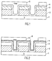
- a typical feature requiring high oxide to nitride selectivity consisting of a silicon substrate 1 with gate electrodes 2, being about 200-800 nm in thickness.
- the gate electrodes 2 have a nitride cap 3, and electrodes and substrate are lined with a thin conformal nitride layer 4, which is usually between 10-100 nm in thickness.
- These features are then filled with a dielectric 5, such as silicon dioxide, planarized, and patterned with photo resist and etched.
- a stoichiometrically altered nitride layer as either all or part of the conformal nitride layer is introduced.
- a feature having a silicon substrate 1 gate electrodes 2, cap 3 and conformal nitride 4 layers is constructed.
- An altered conformal nitride layer 6 is added.
- This structure can be constructed having the altered conformal nitride layer 6 replacing the first conformal nitride layer 4.
- This same type of altered nitride could additionally be included in the cap 3 of the gate electrode 2.
- This nitride layer consists of higher concentrations of some materials, such as silicon and hydrogen, which add substantial selectivity to the nitride film during the etch process, without substantially changing the dielectric properties of the material.
- High selectivity oxide etch processes are commonly known throughout the semiconductor industry. Specifically, selectivities to silicon greater than 40:1 have been obtained on planar surfaces. These types of selectivities can be readily achieved in advanced etch systems, such as the AME Centura Oxide Etcher, because of their independent RF biasing, low pressure, and low fluorine content polymers when scavenging media are employed. High selectivity to polysilicon, for example, can even be obtained over topography for extended overetch times. This is noteworthy because when topography is introduced, ions impinging on exposed corners act to remove the deposited polymer, allowing sputtering of the polysilicon corner.
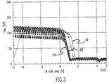
- the Si 3 N 4 composition is altered such that it contains a higher percentage of silicon, in the range of 43.1 to 65 atomic percent.
- the material is insulating throughout this range as revealed by current-voltage characteristics as is shown in the graph of Figure 3.
- the bottom most curve represents a sample having 43.1 atomic percent silicon and the top most curve represents a sample having 67 atomic percent silicon.
- the refractive index for samples having 43 to 60% atomic percent of silicon ranged from 1.90 to 2.11.
- Samples having 65 to 67 atomic percent silicon had a refractive index of 2.20.
- charge trapping which can have a detrimental effect on device stability, becomes more severe at the higher silicon levels as seen from the shift in capacitance-voltage characteristics, shown in the graph of Figure 4.
- This curve represents samples having 43.1 to 67 atomic percent of silicon for a thin, between 30-40 nm, nitride, as well.
- the best concentration range for maximizing etch selectivity while minimizing conductivity is 50 to 60 atomic percent.
- this nitride retains the insulator characteristics which will prevent shorts, it will also have the increased selectivity required for a manufacturable process.
- Adjustment of the nitride stoichiometry is easily accomplished by adjusting the SiH 4 flow with respect to NH 3 or N 2 ratios during a Plasma Enhanced Chemical Vapor Deposition (PECVD) process. Concentrations ranging from about 50-60 atomic percent can be obtained in this manner with minimal process optimization. Stoichiometrically altered nitride films can also be deposited by sputtering or by other chemical vapor deposition processes or can be formed by ion implantation.
- PECVD Plasma Enhanced Chemical Vapor Deposition
- This technique while demonstrated with silicon-rich nitride, can be expanded to include other types of selectivity enhancers. These may include hydrogen, which may act as a polymer source during the etch.
- Other known etch stop materials such as Si 2 O 3 , Al 2 O 3, or Y 2 O 3 , also can be incorporated into a nitride film by sputtering, CVD, or ion implantation, which will allow it to behave as a nitride, but have enough characteristics of the additive film to improve selectivity in an oxide etch chemistry.
- This process adds minimal complexity.
- This stoichiometrically altered film can be added on top of the existing LPCVD nitride, or, if reliability is acceptable, can be used as the sole etch stop, requiring no additional process steps.
- this invention is desirable because it means implementation of a borderless contact process is dependent on a controlled feature, not the etch process alone. While high density plasma etching may be critical to etch high aspect ratios and obtain selectivity to nitride on plana surfaces, it is not in itself a means to obtain a borderless contact.
Landscapes
- Engineering & Computer Science (AREA)
- Manufacturing & Machinery (AREA)
- Physics & Mathematics (AREA)
- Condensed Matter Physics & Semiconductors (AREA)
- General Physics & Mathematics (AREA)
- Computer Hardware Design (AREA)
- Microelectronics & Electronic Packaging (AREA)
- Power Engineering (AREA)
- Inorganic Chemistry (AREA)
- Chemical & Material Sciences (AREA)
- Internal Circuitry In Semiconductor Integrated Circuit Devices (AREA)
- Drying Of Semiconductors (AREA)
- Electrodes Of Semiconductors (AREA)
- Weting (AREA)
Applications Claiming Priority (2)
| Application Number | Priority Date | Filing Date | Title |
|---|---|---|---|
| US08/435,063 US5622596A (en) | 1995-05-08 | 1995-05-08 | High density selective SiO2 :Si3 N4 etching using a stoichiometrically altered nitride etch stop |
| US435063 | 1995-05-08 |
Publications (2)
| Publication Number | Publication Date |
|---|---|
| EP0742584A2 true EP0742584A2 (fr) | 1996-11-13 |
| EP0742584A3 EP0742584A3 (fr) | 1997-10-08 |
Family
ID=23726810
Family Applications (1)
| Application Number | Title | Priority Date | Filing Date |
|---|---|---|---|
| EP96480038A Withdrawn EP0742584A3 (fr) | 1995-05-08 | 1996-04-04 | Gravure sélective à haute densité de SiO2:Si3N4 utilisant une couche d'arrêt d'attaque en nitrure ayant une stoechiométrie modifiée |
Country Status (5)
| Country | Link |
|---|---|
| US (1) | US5622596A (fr) |
| EP (1) | EP0742584A3 (fr) |
| JP (1) | JP3193632B2 (fr) |
| KR (1) | KR100209041B1 (fr) |
| TW (1) | TW301777B (fr) |
Cited By (1)
| Publication number | Priority date | Publication date | Assignee | Title |
|---|---|---|---|---|
| WO2011028461A1 (fr) * | 2009-09-03 | 2011-03-10 | Raytheon Company | Structure semi-conductrice et procédé |
Families Citing this family (15)
| Publication number | Priority date | Publication date | Assignee | Title |
|---|---|---|---|---|
| US6040619A (en) * | 1995-06-07 | 2000-03-21 | Advanced Micro Devices | Semiconductor device including antireflective etch stop layer |
| US5897372A (en) * | 1995-11-01 | 1999-04-27 | Micron Technology, Inc. | Formation of a self-aligned integrated circuit structure using silicon-rich nitride as a protective layer |
| US6004875A (en) | 1995-11-15 | 1999-12-21 | Micron Technology, Inc. | Etch stop for use in etching of silicon oxide |
| US5973385A (en) * | 1996-10-24 | 1999-10-26 | International Business Machines Corporation | Method for suppressing pattern distortion associated with BPSG reflow and integrated circuit chip formed thereby |
| US6136700A (en) * | 1996-12-20 | 2000-10-24 | Texas Instruments Incorporated | Method for enhancing the performance of a contact |
| US6001268A (en) * | 1997-06-05 | 1999-12-14 | International Business Machines Corporation | Reactive ion etching of alumina/TiC substrates |
| US5880005A (en) * | 1997-10-23 | 1999-03-09 | Taiwan Semiconductor Manufacturing Company, Ltd. | Method for forming a tapered profile insulator shape |
| US6207575B1 (en) * | 1998-02-20 | 2001-03-27 | Advanced Micro Devices, Inc. | Local interconnect etch characterization using AFM |
| US6602434B1 (en) * | 1998-03-27 | 2003-08-05 | Applied Materials, Inc. | Process for etching oxide using hexafluorobutadiene or related fluorocarbons and manifesting a wide process window |
| US6063711A (en) * | 1998-04-28 | 2000-05-16 | Taiwan Semiconductor Manufacturing Company | High selectivity etching stop layer for damascene process |
| US5880006A (en) * | 1998-05-22 | 1999-03-09 | Vlsi Technology, Inc. | Method for fabrication of a semiconductor device |
| US6316349B1 (en) * | 1998-11-12 | 2001-11-13 | Hyundai Electronics Industries Co., Ltd. | Method for forming contacts of semiconductor devices |
| US6268299B1 (en) | 2000-09-25 | 2001-07-31 | International Business Machines Corporation | Variable stoichiometry silicon nitride barrier films for tunable etch selectivity and enhanced hyrogen permeability |
| US20040175934A1 (en) * | 2003-03-04 | 2004-09-09 | International Business Machines Corporation | Method for improving etch selectivity effects in dual damascene processing |
| US20060045986A1 (en) * | 2004-08-30 | 2006-03-02 | Hochberg Arthur K | Silicon nitride from aminosilane using PECVD |
Family Cites Families (13)
| Publication number | Priority date | Publication date | Assignee | Title |
|---|---|---|---|---|
| US4299862A (en) * | 1979-11-28 | 1981-11-10 | General Motors Corporation | Etching windows in thick dielectric coatings overlying semiconductor device surfaces |
| US4367119A (en) * | 1980-08-18 | 1983-01-04 | International Business Machines Corporation | Planar multi-level metal process with built-in etch stop |
| US4447824A (en) * | 1980-08-18 | 1984-05-08 | International Business Machines Corporation | Planar multi-level metal process with built-in etch stop |
| JPS6010644A (ja) * | 1983-06-30 | 1985-01-19 | Toshiba Corp | 半導体装置の製造方法 |
| US4656729A (en) * | 1985-03-25 | 1987-04-14 | International Business Machines Corp. | Dual electron injection structure and process with self-limiting oxidation barrier |
| JPS62205645A (ja) * | 1986-03-06 | 1987-09-10 | Fujitsu Ltd | 半導体装置の製造方法 |
| EP0265584A3 (fr) * | 1986-10-30 | 1989-12-06 | International Business Machines Corporation | Méthode et procédé pour l'attaque du bioxyde de silicium utilisant du nitrure de silicium ou du bioxyde de silicium riche en silicium comme barière d'attaque |
| US5443998A (en) * | 1989-08-01 | 1995-08-22 | Cypress Semiconductor Corp. | Method of forming a chlorinated silicon nitride barrier layer |
| US5468987A (en) * | 1991-03-06 | 1995-11-21 | Semiconductor Energy Laboratory Co., Ltd. | Semiconductor device and method for forming the same |
| EP0523856A3 (en) * | 1991-06-28 | 1993-03-17 | Sgs-Thomson Microelectronics, Inc. | Method of via formation for multilevel interconnect integrated circuits |
| US5252515A (en) * | 1991-08-12 | 1993-10-12 | Taiwan Semiconductor Manufacturing Company | Method for field inversion free multiple layer metallurgy VLSI processing |
| US5252516A (en) * | 1992-02-20 | 1993-10-12 | International Business Machines Corporation | Method for producing interlevel stud vias |
| US5324690A (en) * | 1993-02-01 | 1994-06-28 | Motorola Inc. | Semiconductor device having a ternary boron nitride film and a method for forming the same |
-
1995
- 1995-05-08 US US08/435,063 patent/US5622596A/en not_active Expired - Fee Related
-
1996
- 1996-01-16 TW TW085100436A patent/TW301777B/zh active
- 1996-04-04 EP EP96480038A patent/EP0742584A3/fr not_active Withdrawn
- 1996-04-23 KR KR1019960012358A patent/KR100209041B1/ko not_active Expired - Fee Related
- 1996-04-30 JP JP10911196A patent/JP3193632B2/ja not_active Expired - Fee Related
Cited By (2)
| Publication number | Priority date | Publication date | Assignee | Title |
|---|---|---|---|---|
| WO2011028461A1 (fr) * | 2009-09-03 | 2011-03-10 | Raytheon Company | Structure semi-conductrice et procédé |
| US9293379B2 (en) | 2009-09-03 | 2016-03-22 | Raytheon Company | Semiconductor structure with layers having different hydrogen contents |
Also Published As
| Publication number | Publication date |
|---|---|
| TW301777B (fr) | 1997-04-01 |
| US5622596A (en) | 1997-04-22 |
| KR960042996A (ko) | 1996-12-21 |
| EP0742584A3 (fr) | 1997-10-08 |
| KR100209041B1 (ko) | 1999-07-15 |
| JPH08306658A (ja) | 1996-11-22 |
| JP3193632B2 (ja) | 2001-07-30 |
Similar Documents
| Publication | Publication Date | Title |
|---|---|---|
| US5622596A (en) | High density selective SiO2 :Si3 N4 etching using a stoichiometrically altered nitride etch stop | |
| US6162737A (en) | Films doped with carbon for use in integrated circuit technology | |
| US5292673A (en) | Method of manufacturing a semiconductor device | |
| US6541280B2 (en) | High K dielectric film | |
| US5256245A (en) | Use of a clean up step to form more vertical profiles of polycrystalline silicon sidewalls during the manufacture of a semiconductor device | |
| US6831339B2 (en) | Aluminum nitride and aluminum oxide/aluminum nitride heterostructure gate dielectric stack based field effect transistors and method for forming same | |
| US6136700A (en) | Method for enhancing the performance of a contact | |
| US4559693A (en) | Process for fabricating field effect transistors | |
| EP0050973B1 (fr) | Procédé de masquage pour dispositif semiconducteurs utilisant une couche de polymère | |
| US6239011B1 (en) | Method of self-aligned contact hole etching by fluorine-containing discharges | |
| US5963810A (en) | Semiconductor device having nitrogen enhanced high permittivity gate insulating layer and fabrication thereof | |
| KR0172116B1 (ko) | 반도체 장치의 제조방법 | |
| US20080079083A1 (en) | Semiconductor device and a method of manufacture therefor | |
| US6417083B1 (en) | Methods for manufacturing semiconductor devices | |
| US6992020B2 (en) | Method of fabricating semiconductor device | |
| US20040150056A1 (en) | Gate metal recess for oxidation protection and parasitic capacitance reduction | |
| KR20000001625A (ko) | 2중층 스페이서를 갖는 모스 트랜지스터 형성방법 | |
| US6537906B1 (en) | Methods for fabricating semiconductor devices | |
| US6441464B1 (en) | Gate oxide stabilization by means of germanium components in gate conductor | |
| US6191016B1 (en) | Method of patterning a layer for a gate electrode of a MOS transistor | |
| KR20050058613A (ko) | 메모리 소자 및 그 제조 방법 | |
| US20050136688A1 (en) | Method of inhibiting degradation of gate oxide film | |
| JP2001102455A (ja) | 半導体デバイスの誘電体層内に接点用開口を形成する方法。 | |
| KR100266635B1 (ko) | 반도체산화막형성방법 | |
| KR100866119B1 (ko) | 듀얼 게이트 전극 형성방법 |
Legal Events
| Date | Code | Title | Description |
|---|---|---|---|
| PUAI | Public reference made under article 153(3) epc to a published international application that has entered the european phase |
Free format text: ORIGINAL CODE: 0009012 |
|
| AK | Designated contracting states |
Kind code of ref document: A2 Designated state(s): DE FR GB |
|
| 17P | Request for examination filed |
Effective date: 19970325 |
|
| PUAL | Search report despatched |
Free format text: ORIGINAL CODE: 0009013 |
|
| AK | Designated contracting states |
Kind code of ref document: A3 Designated state(s): DE FR GB |
|
| STAA | Information on the status of an ep patent application or granted ep patent |
Free format text: STATUS: THE APPLICATION HAS BEEN WITHDRAWN |
|
| 18W | Application withdrawn |
Withdrawal date: 19971223 |