EP0735480A1 - Cache-kohärentes Computersystem, das Entwertungs- und Rückschreiboperationen minimiert - Google Patents
Cache-kohärentes Computersystem, das Entwertungs- und Rückschreiboperationen minimiert Download PDFInfo
- Publication number
- EP0735480A1 EP0735480A1 EP96301803A EP96301803A EP0735480A1 EP 0735480 A1 EP0735480 A1 EP 0735480A1 EP 96301803 A EP96301803 A EP 96301803A EP 96301803 A EP96301803 A EP 96301803A EP 0735480 A1 EP0735480 A1 EP 0735480A1
- Authority
- EP
- European Patent Office
- Prior art keywords
- read
- share
- tags
- datablock
- request
- Prior art date
- Legal status (The legal status is an assumption and is not a legal conclusion. Google has not performed a legal analysis and makes no representation as to the accuracy of the status listed.)
- Granted
Links
Images


Classifications
-
- G—PHYSICS
- G06—COMPUTING OR CALCULATING; COUNTING
- G06F—ELECTRIC DIGITAL DATA PROCESSING
- G06F12/00—Accessing, addressing or allocating within memory systems or architectures
- G06F12/02—Addressing or allocation; Relocation
- G06F12/08—Addressing or allocation; Relocation in hierarchically structured memory systems, e.g. virtual memory systems
- G06F12/0802—Addressing of a memory level in which the access to the desired data or data block requires associative addressing means, e.g. caches
- G06F12/0806—Multiuser, multiprocessor or multiprocessing cache systems
- G06F12/0815—Cache consistency protocols
- G06F12/0817—Cache consistency protocols using directory methods
- G06F12/0822—Copy directories
-
- G—PHYSICS
- G06—COMPUTING OR CALCULATING; COUNTING
- G06F—ELECTRIC DIGITAL DATA PROCESSING
- G06F12/00—Accessing, addressing or allocating within memory systems or architectures
- G06F12/02—Addressing or allocation; Relocation
- G06F12/08—Addressing or allocation; Relocation in hierarchically structured memory systems, e.g. virtual memory systems
- G06F12/0802—Addressing of a memory level in which the access to the desired data or data block requires associative addressing means, e.g. caches
- G06F12/0806—Multiuser, multiprocessor or multiprocessing cache systems
- G06F12/0815—Cache consistency protocols
Definitions
- the present invention pertains to the field of computer systems. More particularly, this invention relates to a multiprocessor computer system including a mechanism for reducing the occurrences of invalidation operations and copyback operations for maintaining data coherency.
- Prior multiprocessor computer systems typically include a set of processor subsystems coupled to a main memory subsystem.
- a main memory subsystem typically provides instruction and data storage areas for the processors in the system, as well as storage areas for data structures that are shared among the processors of the system.
- shared data structures enable inter processor communication and data and code sharing between the processors.
- the processor subsystems are coupled to the main memory subsystem via a physical interconnect such as a common bus or a switched interconnect data path.
- a physical interconnect such as a common bus or a switched interconnect data path.
- Such an interconnection may function as either a simple circuit switched interconnection or a more complex packet switched interconnection that enables out of order transactions.
- each processor subsystem typically includes an associated extemal cache memory.
- an extemal cache memory usually stores selected data blocks from the main memory subsystem.
- an external cache memory provides fast processor access to the cached data blocks by avoiding fetches to the main memory subsystem for datablocks that are stored in the cache.
- Such a multiprocessor computer system typically implements a protocol for maintaining data coherency between the main memory and the corresponding datablocks stored in the cache memories.
- Each cache memory typically includes a set of tags that indicate the status of the cached datablocks.
- the MOESI protocol maintains a set of five states for datablocks stored in the cache memories.
- the states include an "invalid" state, a "shared” state, an "exclusive” state, and a "modified" state.
- a first processor executes a load memory instruction targeted for a datablock that is not in the extemal cache for the first processor then the appropriate datablock is externally fetched.
- the first processor issues a read_to_share (RDS) transaction that specifies the missing datablock to the memory interconnect.
- RDS read_to_share
- Such a read_to_share (RDS) transaction usually returns the missing datablock to the external cache of the first processor and the tags associated with that datablock in the external cache of the first processor are modified to indicate that the datablock is cached in a "shared" state.
- a multiprocessor computer system may implement a first write optimization to such a MOESI protocol.
- a read_to_share (RDS) transaction from the first processor returns the missing datablock and modifies the tags associated with the missing datablock to indicate the "exclusive" state if no other cache memory owns the datablock. Thereafter, if the first processor executes store instructions to that exclusive datablock then no other cache coherency messages are transferred through the memory interconnect.
- RDS read_to_share
- Such a write optimization to the MOESI protocol is usually based on an assumption that a read_to_share (RDS) transaction from the first processor targeted for a datablock not owned by any other processor corresponds to a private datablock for the first processor. If such an assumption is wrong and the missing datablock is not private data then a second processor may later issue a read_to_share (RDS) transaction through the memory interconnect for that datablock. In such a case, the first processor must usually supply the missing datablock to the second processor on a copyback operation even though the first processor may not have modified the datablock and even though the missing datablock is available from main memory.
- RDS read_to_share
- a computer system that selectively enables and disables a first write optimization of a cache coherency protocol for data that is not likely to be written by a requesting processor.
- the disabling of the first write optimization reduces copyback and invalidation messages in a multiprocessor system during cache misses to read-only memory pages or instruction fetches.
- Advantages are realized in computer systems that share instructions among processors in read-only code segments such as may be found with dynamic link libraries. Advantages are also realized for shared read-only constant data and for process migration from processor to processor.
- the computer system includes a set of processor subsystems and a memory interconnect.
- Each processor subsystems includes an extemal cache memory including external tags and the memory interconnect maintains a set of duplicate tags that correspond to the extemal tags.
- a processor subsystem generates a read to share always (RDSA) request upon a cache miss to a read-only datablock and generates a read to share (RDS) request otherwise.
- the memory interconnect enables access to a shared memory and controls the cache state transitions of the external tags and the duplicate tags to selectively enable or disable the first write optimization.
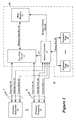
- FIG. 1 illustrates a computer system 10 for one embodiment.
- the computer system 10 comprises a set of processor subsystems 20-22 and a memory interconnect subsystem 18.
- Each of the processor subsystems 20-22 includes an L2 cache memory.
- the memory interconnect subsystem 18 provides shared access to a main memory 14 to the processor subsystems 20-22.
- the processor subsystems 20-22 communicate with the memory interconnect subsystem 18 via a set of memory ports 1-N.
- port 1 for the processor subsystem 20 comprises a data path 40, an address path 42, and a control path 44
- port N for the processor subsystem 22 comprises a data path 46, an address path 48 and a control path 50.
- the memory interconnect subsystem 18 includes a data path switch 12 to the main memory 14, a system controller 16, and a set of duplicate tags 30-32.
- the data path switch 12 is a cross bar switch controlled by the system controller 16 via a set of control signals 54.
- the data path switch 12 enables data path access to the main memory 14 via the data path of each port IN including the data path 40 and the data path 46.
- the system controller 16 functions as a memory controller by decoding the addresses received from the processor subsystems 20-22 and by generating memory control signals including row address select (RAS) and column address select (CAS) signals to the main memory 14 via a memory control bus 56.
- RAS row address select
- CAS column address select
- the system controller 16 also implements a cache coherency mechanism for the computer system 10.
- the system controller 16 maintains sets of duplicate tags 30-32.
- the duplicate tags 30-32 reflect the tags corresponding to the external caches of the processor subsystems 20-22.
- the duplicate tags 30 correspond to the tags of the extemal cache memory in the processor subsystem 20 and the duplicate tags 32 reflect the information stored in the tags of the external cache memory in the processor subsystem 22.
- the system controller 16 performs tag look up and tag modify operations to the duplicate tags 30-32 via a snoop bus 58.
- the system controller 16 receives memory access requests from the processor subsystems 20-22 via the address path of each port 1-N including the address path 42 and the address path 48.
- the system controller 16 arbitrates among the requests from the processor subsystems 20-22 and configures the data path switch 12 to provide the necessary connections for access to the main memory 14 via a memory data bus 52 or for processor subsystem to processor subsystem data transfers.
- the system controller 16 responds with cache state transition control messages and other information via the appropriate control path.
- the memory access requests include, for example, read_to_share (RDS) requests and read_to_share_always (RDSA) requests.
- the processor subsystems 20-22 use a read_to_share (RDS) request to the system controller 16 to retrieve a missing cache block after a load miss to the corresponding external cache memory if the load is targeted for read-write data.
- the processor subsystems 20-22 use a read_to_share_always (RDSA) request to the system controller 16 to retrieve a missing cache block after a load miss to the corresponding external cache memory if the load is targeted for read-only data such as instruction code or other types of data not likely to be written.
- Such read only misses may correspond to instruction cache misses or data cache misses data marked as read-only by a memory management mechanism.
- the system controller 16 processes a read_to_share (RDS) or a read_to_share_always (RDSA) request by performing a tag lookup on the spedfied datablock via the snoop bus 58.
- the system controller 16 reads the duplicate tags 30-32 via the snoop bus 58 to determine the cache state of the spedfied datablock.
- the system controller 16 configures the data path switch 12 to provide the proper source for the specified datablock for the read_to_share (RDS) or the read_to_share_always (RDSA) transaction.
- the appropriate source may include, for example, the main memory 14 or one of the external caches of the processor subsystems 20-22 according to the state of the duplicate tags 30-32.
- the system controller 16 transfers messages via the control path of the ports 1-N to control the cache state transitions in the processor subsystems 20-22 involved in the read_to_share (RDS) or read_to_share_always (RDSA) transaction.
- the system controller 16 also updates the cache states via the snoop bus 58 for the duplicate tags 30-32 involved in the read_to_share (RDS) or read_to_share_always (RDSA) transaction.
- Figure 2 illustrates the cache coherency protocol of the duplicate tags 30-32 for one embodiment.
- the system controller 16 maintains the duplicate tags 30-32 according to an MOSI cache coherency protocol which includes an "invalid" (I) state, a “shared clean” (S) state, a “shared modified” (O) state, and an "exclusive and potentially modified” (M) state.
- I invalid
- S shared clean
- O shared modified
- M exclusive and potentially modified
- FIG. 3 illustrates the processor subsystem 20 for one embodiment.
- the processor subsystem 20 comprises a processor 70, an external cache 74, and associated set of extemal tags 76, and a port interface 72.
- Other processor subsystems in the computer system 10, such as the processor subsystem 22, may be implemented in a similar fashion as that shown for the processor subsystem 20.
- the processor 70 issues memory load and memory store operations to the external cache 74.
- a cache "miss" to the external cache 74 causes the port interface 72 to issue a cache request to the system controller 16 using a message packet transferred via the address path 42.
- the cache requests issued include, for example, read_to_share_always (RDSA) and read_to_share (RDS) cache requests.
- the message packet transferred via the address path 42 includes a header that specifies the request type and an address that specifies the datablock of the cache request.
- the port interface 72 receives the missing datablock via the data path 40.
- the port interface 72 receives cache state control messages from the system controller 16 via the control path 44.
- the cache state control messages determine the cache state transitions for the newly fetched missing datablock stored in the external cache 74.
- FIG. 4 illustrates the cache coherency protocol of the external tags 76 for one embodiment.
- the external cache 74 maintains the extemal tags 76 according to an MOESI cache coherency protocol which includes an "invalid" (I) state, a "shared clean” (S) state, an "exclusive clean” (E) state, a “shared modified” (O) state, and an "exclusive modified” (M) state.
- I invalid
- S shared clean
- E exclusive clean
- O shared modified
- M exclusive modified
- the external cache 74 maintains the extemal tags 76 according to an MESI cache coherency protocol while the system controller 16 maintains the duplicate tags 30-32 according to an MSI cache coherency protocol.
- the memory interconnect subsystem 18 enables the memory interconnect subsystem 18 to function as a reflective memory wherein a copyback operation on a load miss to a "modified" datablock causes the datablock to be written back into the main memory 14 and causes the requesting processor to transition to the "shared" state.
- FIG. 5 illustrates the handling of a read_to_share (RDS) transaction with write optimization by the system controller 16.
- the write optimization illustrated may be referred to as a first write optimization to the cache coherence protocol of the computer system 10.
- the system controller 16 receives a read_to_share (RDS) transaction from one of the processor subsystems 20-22 coupled to one of the memory ports 1-N hereinafter referred to as memory Port A.
- RDS read_to_share
- the system controller 16 reads the duplicate tags that correspond to the memory Port A via the snoop bus 58 for the specified datablock of the read_to_share (RDS) transaction.
- RDS read_to_share
- the system controller 16 configures the data path switch 12 to supply the read data for the specified datablock to satisfy the read_to_share (RDS) transaction.
- the read data for the specified datablock is supplied to Port A from the main memory 14.
- the system controller 16 transfers a message via the Port A control path that causes the Port A external tags to transition from the "invalid” (I) state to the "exclusive clean” (E) state for the specified datablock.
- the system controller 16 sets the duplicate tags for Port A from the "invalid” (I) to the "exclusive and potentially modified” state for the datablock via the snoop bus 58.
- a read transaction issued from another memory port and targeted for the same datablock as the read_to_share (RDS) transaction above causes the system controller 16 to issue a copyback request to the memory Port A because the duplicate tags for Port A indicate the "exclusive and potentially modified" state for the datablock.
- Such a copyback operation occurs whether or not the processor of Port A has modified that datablock. As a consequence, such a copyback operation may be unnecessary to maintain data coherency in the computer system 10.
- Figure 6 illustrates the handling of a read_to_share_always (RDSA) transaction from Port A by the system controller 16.
- the system controller 16 receives a read_to_share_always (RDSA) request from the memory Port A.
- RDSA read_to_share_always
- the system controller 16 reads the duplicate tags that correspond to the memory Port A via the snoop bus 58 for the specified datablock of the read_to_share_always (RDSA) transaction.
- RDSA read_to_share_always
- the system controller 16 configures the data path switch 12 to supply the read data for the specified datablock to satisfy the read_to_share_always (RDSA) transaction.
- the read data for the specified datablock is supplied to Port A from the main memory 14.
- the system controller 16 transfers a message to the memory Port A via the Port A control path that causes the external tags to transition from the "invalid" (I) state to the "shared clean” (S) state for the specified datablock.
- the system controller 16 sets Port A duplicate tags to the "shared clean" (S) state for the specified datablock via the snoop bus 58.
- control proceeds to block 122. If the specified datablock is held by another port in one of the modified states M or O, then the system controller issues a copyback request at block 130 to the appropriate port to supply the datablock to Port A, and control then proceeds to block 124 to update the external and duplicate tags as described above.
- a read transaction issued from another memory port and targeted for the same datablock as the read_to_share_always (RDSA) transaction above the system controller 16 does not cause a copyback request to the memory Port A because the duplicate tags for Port A indicate the "shared clean" (S) state for the datablock. Since the read_to_share_always (RDSA) transaction is issued only for read-only data, it follows that the corresponding datablock in the Port A external cache remains in the "shared clean" (S) state. As a consequence, an unnecessary copyback operation is avoided while data coherency in the computer system 10 is maintained.
Landscapes
- Engineering & Computer Science (AREA)
- Theoretical Computer Science (AREA)
- Physics & Mathematics (AREA)
- General Engineering & Computer Science (AREA)
- General Physics & Mathematics (AREA)
- Memory System Of A Hierarchy Structure (AREA)
Applications Claiming Priority (2)
| Application Number | Priority Date | Filing Date | Title |
|---|---|---|---|
| US42301695A | 1995-03-31 | 1995-03-31 | |
| US423016 | 1995-03-31 |
Publications (2)
| Publication Number | Publication Date |
|---|---|
| EP0735480A1 true EP0735480A1 (de) | 1996-10-02 |
| EP0735480B1 EP0735480B1 (de) | 2003-06-04 |
Family
ID=23677349
Family Applications (1)
| Application Number | Title | Priority Date | Filing Date |
|---|---|---|---|
| EP96301803A Expired - Lifetime EP0735480B1 (de) | 1995-03-31 | 1996-03-15 | Cache-kohärentes Computersystem, das Entwertungs- und Rückschreiboperationen minimiert |
Country Status (5)
| Country | Link |
|---|---|
| US (1) | US5706463A (de) |
| EP (1) | EP0735480B1 (de) |
| JP (1) | JP3784101B2 (de) |
| DE (1) | DE69628493T2 (de) |
| SG (1) | SG45415A1 (de) |
Cited By (2)
| Publication number | Priority date | Publication date | Assignee | Title |
|---|---|---|---|---|
| EP1620804A2 (de) * | 2003-04-02 | 2006-02-01 | Intel Corporation | Zuordnung von cachespeicher bei einer datenplazierung in einer netzwerkschnittstelle |
| US8327081B2 (en) | 2006-02-28 | 2012-12-04 | Fujitsu Limited | Information processing device and method for controlling the same |
Families Citing this family (38)
| Publication number | Priority date | Publication date | Assignee | Title |
|---|---|---|---|---|
| JPH09204403A (ja) * | 1996-01-26 | 1997-08-05 | Hitachi Ltd | 並列計算機 |
| US6098152A (en) * | 1997-10-17 | 2000-08-01 | International Business Machines Corporation | Method and apparatus for miss sequence cache block replacement utilizing a most recently used state |
| US6341337B1 (en) * | 1998-01-30 | 2002-01-22 | Sun Microsystems, Inc. | Apparatus and method for implementing a snoop bus protocol without snoop-in and snoop-out logic |
| US6397302B1 (en) * | 1998-06-18 | 2002-05-28 | Compaq Information Technologies Group, L.P. | Method and apparatus for developing multiprocessor cache control protocols by presenting a clean victim signal to an external system |
| US6378048B1 (en) * | 1998-11-12 | 2002-04-23 | Intel Corporation | “SLIME” cache coherency system for agents with multi-layer caches |
| US6857051B2 (en) * | 1998-12-23 | 2005-02-15 | Intel Corporation | Method and apparatus for maintaining cache coherence in a computer system |
| US6374333B1 (en) * | 1999-11-09 | 2002-04-16 | International Business Machines Corporation | Cache coherency protocol in which a load instruction hint bit is employed to indicate deallocation of a modified cache line supplied by intervention |
| US6345342B1 (en) * | 1999-11-09 | 2002-02-05 | International Business Machines Corporation | Cache coherency protocol employing a read operation including a programmable flag to indicate deallocation of an intervened cache line |
| US6349369B1 (en) * | 1999-11-09 | 2002-02-19 | International Business Machines Corporation | Protocol for transferring modified-unsolicited state during data intervention |
| US6345344B1 (en) * | 1999-11-09 | 2002-02-05 | International Business Machines Corporation | Cache allocation mechanism for modified-unsolicited cache state that modifies victimization priority bits |
| US6345343B1 (en) * | 1999-11-09 | 2002-02-05 | International Business Machines Corporation | Multiprocessor system bus protocol with command and snoop responses for modified-unsolicited cache state |
| US6519685B1 (en) * | 1999-12-22 | 2003-02-11 | Intel Corporation | Cache states for multiprocessor cache coherency protocols |
| US6745297B2 (en) * | 2000-10-06 | 2004-06-01 | Broadcom Corporation | Cache coherent protocol in which exclusive and modified data is transferred to requesting agent from snooping agent |
| US20030115402A1 (en) * | 2001-11-16 | 2003-06-19 | Fredrik Dahlgren | Multiprocessor system |
| US20040117669A1 (en) * | 2002-12-12 | 2004-06-17 | Wilson Peter A. | Method for controlling heat dissipation of a microprocessor |
| US7284097B2 (en) * | 2003-09-30 | 2007-10-16 | International Business Machines Corporation | Modified-invalid cache state to reduce cache-to-cache data transfer operations for speculatively-issued full cache line writes |
| US7818391B2 (en) | 2004-01-20 | 2010-10-19 | Hewlett-Packard Development Company, L.P. | System and method to facilitate ordering point migration |
| US8145847B2 (en) * | 2004-01-20 | 2012-03-27 | Hewlett-Packard Development Company, L.P. | Cache coherency protocol with ordering points |
| US7769959B2 (en) | 2004-01-20 | 2010-08-03 | Hewlett-Packard Development Company, L.P. | System and method to facilitate ordering point migration to memory |
| US8176259B2 (en) | 2004-01-20 | 2012-05-08 | Hewlett-Packard Development Company, L.P. | System and method for resolving transactions in a cache coherency protocol |
| US8468308B2 (en) * | 2004-01-20 | 2013-06-18 | Hewlett-Packard Development Company, L.P. | System and method for non-migratory requests in a cache coherency protocol |
| US7620696B2 (en) * | 2004-01-20 | 2009-11-17 | Hewlett-Packard Development Company, L.P. | System and method for conflict responses in a cache coherency protocol |
| US7395374B2 (en) * | 2004-01-20 | 2008-07-01 | Hewlett-Packard Company, L.P. | System and method for conflict responses in a cache coherency protocol with ordering point migration |
| US8090914B2 (en) * | 2004-01-20 | 2012-01-03 | Hewlett-Packard Development Company, L.P. | System and method for creating ordering points |
| US20050160238A1 (en) * | 2004-01-20 | 2005-07-21 | Steely Simon C.Jr. | System and method for conflict responses in a cache coherency protocol with ordering point migration |
| US8332592B2 (en) * | 2004-10-08 | 2012-12-11 | International Business Machines Corporation | Graphics processor with snoop filter |
| WO2007094038A1 (ja) * | 2006-02-13 | 2007-08-23 | Fujitsu Limited | システム制御装置、キャッシュ制御装置およびキャッシュ状態遷移制御方法 |
| US20070283095A1 (en) * | 2006-06-06 | 2007-12-06 | Alcor Micro, Corp. | Method to access storage device through universal serial bus |
| JP4912790B2 (ja) * | 2006-08-18 | 2012-04-11 | 富士通株式会社 | システムコントローラ,スヌープタグ更新方法および情報処理装置 |
| US7613882B1 (en) | 2007-01-29 | 2009-11-03 | 3 Leaf Systems | Fast invalidation for cache coherency in distributed shared memory system |
| JP5393964B2 (ja) * | 2007-09-11 | 2014-01-22 | 中菱エンジニアリング株式会社 | 車両試験装置 |
| JP5568939B2 (ja) | 2009-10-08 | 2014-08-13 | 富士通株式会社 | 演算処理装置及び制御方法 |
| US8904115B2 (en) * | 2010-09-28 | 2014-12-02 | Texas Instruments Incorporated | Cache with multiple access pipelines |
| JP5974720B2 (ja) * | 2012-08-09 | 2016-08-23 | 富士通株式会社 | 演算処理装置、情報処理装置および情報処理装置の制御方法 |
| JP5971036B2 (ja) * | 2012-08-30 | 2016-08-17 | 富士通株式会社 | 演算処理装置及び演算処理装置の制御方法 |
| CN106681938B (zh) * | 2012-10-22 | 2020-08-18 | 英特尔公司 | 用于控制多时隙链路层微片中的消息收发的装置和系统 |
| US9584617B2 (en) * | 2013-12-31 | 2017-02-28 | Successfactors, Inc. | Allocating cache request in distributed cache system based upon cache object and marker identifying mission critical data |
| US9823730B2 (en) * | 2015-07-08 | 2017-11-21 | Apple Inc. | Power management of cache duplicate tags |
Citations (4)
| Publication number | Priority date | Publication date | Assignee | Title |
|---|---|---|---|---|
| EP0358863A2 (de) * | 1988-09-16 | 1990-03-21 | Digital Equipment Corporation | Laden/Speichern mit Schreibabsicht für Nachschreib-Cache-Speicher |
| US4977498A (en) * | 1988-04-01 | 1990-12-11 | Digital Equipment Corporation | Data processing system having a data memory interlock coherency scheme |
| EP0507063A1 (de) * | 1991-04-03 | 1992-10-07 | International Business Machines Corporation | Verfahren und Vorrichtung für ein Verzeichnis zum kreuzweisen Ungültigerklären |
| US5297269A (en) * | 1990-04-26 | 1994-03-22 | Digital Equipment Company | Cache coherency protocol for multi processor computer system |
Family Cites Families (13)
| Publication number | Priority date | Publication date | Assignee | Title |
|---|---|---|---|---|
| US4228503A (en) * | 1978-10-02 | 1980-10-14 | Sperry Corporation | Multiplexed directory for dedicated cache memory system |
| JPH065524B2 (ja) * | 1987-11-18 | 1994-01-19 | インターナショナル・ビジネス・マシーンズ・コーポレーション | 記憶装置管理方法 |
| EP0380842A3 (de) * | 1989-02-03 | 1991-06-12 | Digital Equipment Corporation | Verfahren und Vorrichtung zur Schnittstellenbildung zwischen einer Systemsteuereinheit für ein Multiprozessorsystem und den zentralen Verarbeitungseinheiten |
| US5036459A (en) * | 1989-03-09 | 1991-07-30 | U.S. Philips Corporation | Multi-processor computer system with distributed memory and an interprocessor communication mechanism, and method for operating such mechanism |
| EP0468831B1 (de) * | 1990-06-29 | 1997-10-15 | Digital Equipment Corporation | Busprotokoll für Prozessor mit write-back cache |
| JPH04318654A (ja) * | 1991-02-13 | 1992-11-10 | Hewlett Packard Co <Hp> | マイクロプロセッサへの割り込みのリダイレクションシステム |
| US5303362A (en) * | 1991-03-20 | 1994-04-12 | Digital Equipment Corporation | Coupled memory multiprocessor computer system including cache coherency management protocols |
| JP2703417B2 (ja) * | 1991-04-05 | 1998-01-26 | 富士通株式会社 | 受信バッファ |
| AU2270892A (en) * | 1991-06-26 | 1993-01-25 | Ast Research, Inc. | Automatic distribution of interrupts controller for a multiple processor computer system |
| DE69230428T2 (de) * | 1991-09-27 | 2000-08-03 | Sun Microsystems, Inc. | Verklemmungserkennung und Maskierung enthaltende Busarbitrierungsarchitektur |
| US5319753A (en) * | 1992-09-29 | 1994-06-07 | Zilog, Inc. | Queued interrupt mechanism with supplementary command/status/message information |
| US5434993A (en) * | 1992-11-09 | 1995-07-18 | Sun Microsystems, Inc. | Methods and apparatus for creating a pending write-back controller for a cache controller on a packet switched memory bus employing dual directories |
| JPH07105031A (ja) * | 1993-09-20 | 1995-04-21 | Internatl Business Mach Corp <Ibm> | 多重プロセッサ・コンピュータ・システム内で割込み情報を伝えるための方法および装置 |
-
1996
- 1996-03-15 DE DE69628493T patent/DE69628493T2/de not_active Expired - Fee Related
- 1996-03-15 EP EP96301803A patent/EP0735480B1/de not_active Expired - Lifetime
- 1996-03-29 JP JP09959496A patent/JP3784101B2/ja not_active Expired - Lifetime
- 1996-03-29 SG SG1996006609A patent/SG45415A1/en unknown
-
1997
- 1997-05-12 US US08/854,418 patent/US5706463A/en not_active Expired - Lifetime
Patent Citations (4)
| Publication number | Priority date | Publication date | Assignee | Title |
|---|---|---|---|---|
| US4977498A (en) * | 1988-04-01 | 1990-12-11 | Digital Equipment Corporation | Data processing system having a data memory interlock coherency scheme |
| EP0358863A2 (de) * | 1988-09-16 | 1990-03-21 | Digital Equipment Corporation | Laden/Speichern mit Schreibabsicht für Nachschreib-Cache-Speicher |
| US5297269A (en) * | 1990-04-26 | 1994-03-22 | Digital Equipment Company | Cache coherency protocol for multi processor computer system |
| EP0507063A1 (de) * | 1991-04-03 | 1992-10-07 | International Business Machines Corporation | Verfahren und Vorrichtung für ein Verzeichnis zum kreuzweisen Ungültigerklären |
Non-Patent Citations (1)
| Title |
|---|
| BORRILL P: "FUTUREBUS PROTOCOLS KEEP CACHE DATA CONSISTENT", COMPUTER TECHNOLOGY REVIEW, vol. 9, no. 10, 21 June 1989 (1989-06-21), pages 36, 38, XP000054499 * |
Cited By (2)
| Publication number | Priority date | Publication date | Assignee | Title |
|---|---|---|---|---|
| EP1620804A2 (de) * | 2003-04-02 | 2006-02-01 | Intel Corporation | Zuordnung von cachespeicher bei einer datenplazierung in einer netzwerkschnittstelle |
| US8327081B2 (en) | 2006-02-28 | 2012-12-04 | Fujitsu Limited | Information processing device and method for controlling the same |
Also Published As
| Publication number | Publication date |
|---|---|
| DE69628493T2 (de) | 2004-05-19 |
| US5706463A (en) | 1998-01-06 |
| EP0735480B1 (de) | 2003-06-04 |
| DE69628493D1 (de) | 2003-07-10 |
| JP3784101B2 (ja) | 2006-06-07 |
| JPH0922383A (ja) | 1997-01-21 |
| SG45415A1 (en) | 1998-01-16 |
Similar Documents
| Publication | Publication Date | Title |
|---|---|---|
| US5706463A (en) | Cache coherent computer system that minimizes invalidation and copyback operations | |
| EP1311955B1 (de) | Verfahren und vorrichtung zur zentralisierten snoop-filterung | |
| US5325504A (en) | Method and apparatus for incorporating cache line replacement and cache write policy information into tag directories in a cache system | |
| CN100428195C (zh) | 数据处理系统和方法 | |
| US7234029B2 (en) | Method and apparatus for reducing memory latency in a cache coherent multi-node architecture | |
| US7747826B2 (en) | Data processing system and method for efficient communication utilizing an in coherency state | |
| US6088769A (en) | Multiprocessor cache coherence directed by combined local and global tables | |
| US8140770B2 (en) | Data processing system and method for predictively selecting a scope of broadcast of an operation | |
| KR101497002B1 (ko) | 스누프 필터링 메커니즘 | |
| KR100273039B1 (ko) | 멀티프로세서 데이터 처리 시스템의 캐쉬 일관성을 유지하기위한 캐쉬 일관성 프로토콜 제공 방법 및시스템 | |
| US5043886A (en) | Load/store with write-intent for write-back caches | |
| US20030195939A1 (en) | Conditional read and invalidate for use in coherent multiprocessor systems | |
| US6859864B2 (en) | Mechanism for initiating an implicit write-back in response to a read or snoop of a modified cache line | |
| US20110029738A1 (en) | Low-cost cache coherency for accelerators | |
| US6405290B1 (en) | Multiprocessor system bus protocol for O state memory-consistent data | |
| JPH08328957A (ja) | マルチプロセッシング・システムにおけるキャッシュ・パフォーマンス向上のためのシステムおよび方法 | |
| US6922755B1 (en) | Directory tree multinode computer system | |
| US20020078305A1 (en) | Method and apparatus for invalidating a cache line without data return in a multi-node architecture | |
| US20040148471A1 (en) | Multiprocessing computer system employing capacity prefetching | |
| KR20090079964A (ko) | 능동적 프리페치들로 향상된 호버 상태를 실시하는 시스템 및 방법 | |
| US6526480B1 (en) | Cache apparatus and control method allowing speculative processing of data | |
| US6678800B1 (en) | Cache apparatus and control method having writable modified state | |
| US20060179249A1 (en) | Data processing system and method for predictively selecting a scope of broadcast of an operation utilizing a location of a memory | |
| EP0735481B1 (de) | Mechanismus auf Systemebene zum Entwerten von Daten, die im externen Cache eines Prozessors in einem Computersystem gespeichert sind | |
| JP2689899B2 (ja) | 情報処理装置 |
Legal Events
| Date | Code | Title | Description |
|---|---|---|---|
| PUAI | Public reference made under article 153(3) epc to a published international application that has entered the european phase |
Free format text: ORIGINAL CODE: 0009012 |
|
| AK | Designated contracting states |
Kind code of ref document: A1 Designated state(s): DE FR GB IT NL SE |
|
| RIN1 | Information on inventor provided before grant (corrected) |
Inventor name: COFFIN III, LOUIS F. Inventor name: KOHN, LESLIE Inventor name: NORMOYLE, KEVIN Inventor name: VAN LOO, WILLIAM Inventor name: NISHTALA, SATYANARAYANA Inventor name: EBRAHIM, ZAHIR |
|
| 17P | Request for examination filed |
Effective date: 19961018 |
|
| 17Q | First examination report despatched |
Effective date: 20000726 |
|
| GRAG | Despatch of communication of intention to grant |
Free format text: ORIGINAL CODE: EPIDOS AGRA |
|
| GRAG | Despatch of communication of intention to grant |
Free format text: ORIGINAL CODE: EPIDOS AGRA |
|
| GRAG | Despatch of communication of intention to grant |
Free format text: ORIGINAL CODE: EPIDOS AGRA |
|
| GRAH | Despatch of communication of intention to grant a patent |
Free format text: ORIGINAL CODE: EPIDOS IGRA |
|
| GRAH | Despatch of communication of intention to grant a patent |
Free format text: ORIGINAL CODE: EPIDOS IGRA |
|
| GRAA | (expected) grant |
Free format text: ORIGINAL CODE: 0009210 |
|
| RAP1 | Party data changed (applicant data changed or rights of an application transferred) |
Owner name: SUN MICROSYSTEMS, INC. |
|
| AK | Designated contracting states |
Designated state(s): DE FR GB IT NL SE |
|
| REG | Reference to a national code |
Ref country code: GB Ref legal event code: FG4D |
|
| REF | Corresponds to: |
Ref document number: 69628493 Country of ref document: DE Date of ref document: 20030710 Kind code of ref document: P |
|
| REG | Reference to a national code |
Ref country code: SE Ref legal event code: TRGR |
|
| PGFP | Annual fee paid to national office [announced via postgrant information from national office to epo] |
Ref country code: FR Payment date: 20040309 Year of fee payment: 9 |
|
| PG25 | Lapsed in a contracting state [announced via postgrant information from national office to epo] |
Ref country code: SE Free format text: LAPSE BECAUSE OF NON-PAYMENT OF DUE FEES Effective date: 20040316 |
|
| PLBE | No opposition filed within time limit |
Free format text: ORIGINAL CODE: 0009261 |
|
| STAA | Information on the status of an ep patent application or granted ep patent |
Free format text: STATUS: NO OPPOSITION FILED WITHIN TIME LIMIT |
|
| ET | Fr: translation filed | ||
| 26N | No opposition filed |
Effective date: 20040305 |
|
| PG25 | Lapsed in a contracting state [announced via postgrant information from national office to epo] |
Ref country code: NL Free format text: LAPSE BECAUSE OF NON-PAYMENT OF DUE FEES Effective date: 20041001 |
|
| EUG | Se: european patent has lapsed | ||
| NLV4 | Nl: lapsed or anulled due to non-payment of the annual fee |
Effective date: 20041001 |
|
| PG25 | Lapsed in a contracting state [announced via postgrant information from national office to epo] |
Ref country code: IT Free format text: LAPSE BECAUSE OF NON-PAYMENT OF DUE FEES;WARNING: LAPSES OF ITALIAN PATENTS WITH EFFECTIVE DATE BEFORE 2007 MAY HAVE OCCURRED AT ANY TIME BEFORE 2007. THE CORRECT EFFECTIVE DATE MAY BE DIFFERENT FROM THE ONE RECORDED. Effective date: 20050315 |
|
| PG25 | Lapsed in a contracting state [announced via postgrant information from national office to epo] |
Ref country code: FR Free format text: LAPSE BECAUSE OF NON-PAYMENT OF DUE FEES Effective date: 20051130 |
|
| REG | Reference to a national code |
Ref country code: FR Ref legal event code: ST Effective date: 20051130 |
|
| PGFP | Annual fee paid to national office [announced via postgrant information from national office to epo] |
Ref country code: DE Payment date: 20070308 Year of fee payment: 12 |
|
| PGFP | Annual fee paid to national office [announced via postgrant information from national office to epo] |
Ref country code: GB Payment date: 20070314 Year of fee payment: 12 |
|
| GBPC | Gb: european patent ceased through non-payment of renewal fee |
Effective date: 20080315 |
|
| PG25 | Lapsed in a contracting state [announced via postgrant information from national office to epo] |
Ref country code: DE Free format text: LAPSE BECAUSE OF NON-PAYMENT OF DUE FEES Effective date: 20081001 |
|
| PG25 | Lapsed in a contracting state [announced via postgrant information from national office to epo] |
Ref country code: GB Free format text: LAPSE BECAUSE OF NON-PAYMENT OF DUE FEES Effective date: 20080315 |